2011年电子科技大学836信号与系统和数字电路真题和答案
数字电路2011期末考试题-参考解答

电子科技大学2010 -2011学年第二学期期末考试 A 卷课程名称:_数字逻辑设计及应用__ 考试形式:闭卷考试日期:20 11 年7 月7 日考试时长:_120___分钟课程成绩构成:平时30 %,期中30 %,实验0 %,期末40 %本试卷试题由__六___部分构成,共__6___页。
I. Fill your answers in the blanks(2’ X 10=20’)1. A parity circuit with N inputs need N-1XOR gate s. If the number of “1” in an N logic variables set, such as A、B、C、…W, is even number, then__________A B C W⊕⊕⊕⋅⋅⋅⋅⊕=0 .2. A circuit with 4 flip-flops can store 4bit binary numbers, that is, include 16 states at most.3. A modulo-20 counter circuit needs 5 D filp-flops at least. A modulo-288 counter circuit needs 3 4-bit counters of 74x163 at least.4. A 8-bit ring counter has 8 normal states. If we want to realize the same number normal states, we need a 4bit twisted-ring counter.5. If the input is 10000000 of an 8 bit DAC, the corresponding output is 5v. Then an input is 00000001 to the DAC, the corresponding output is 5/128 (0.0391) V; if an input is 10001000, the corresponding DAC output is 5.3125V.II. Please select the only one correct answer in the following questions.(2’ X 5=10)B ) chips of 4K ⨯4 bits RAM to form a 16 K ⨯ 8 bits RAM.A) 2 B) 8 C) 4 D) 162. To design a "01101100" serial sequence generator by shift registers, we need a( A)-bit shift register as least.A) 5 B) 4 C) 3 D) 63. For the following latches or flip-flops, ( B) can be used to form shift register.A) S-R latch B) master-slave flip-flop C) S-R latch with enable D) S’-R’ latch4. Which of the following statements is correct? ( C )A) The outputs of a Moore machine depend on inputs as well as the states.B) The outputs of a Mealy machine depend only on the states.C) The outputs of a Mealy machine depend on inputs as well as the states. D) A), B), C) are wrong.5. There is a state/output table of a sequential machine as the table 1, what the input sequences isdetected? ( D )A) 11110 B) 11010 C) 10010 D) 10110Table 1III.Analyze the sequential-circuit as shown in figure 1. [15’]1. Write out the excitation equations, transitionequations and output equation. [5’]2. Assume the initial state is Q 2Q 1=00, complete thetiming diagram for Q 2 ,Q 1 and Z.( Don ’t need consider propagation delay of each component)[10’]Figure-1解答:激励方程: D 1=Q 1⊕Q 2,D 2= Q /1+ Q /2转移方程:Q 1 *= D 1=Q 1⊕Q 2,Q 2 *=D 2= Q /1+ Q /2 输出方程:Z= Q 1•Q 2IV. Design a Mealy sequential detector with one input x and one output z. If and only if xdescribe the state meaning and finish the state/output table. [15] Example : x :0 1 0 1 1 1 1 0 0 1 1 0 0 1 1 1 1 1 z :0 0 0 0 0 0 1 0 0 1 0 0 0 1 0 0 1 1XState meaningS 0 1 Initial A A,0 B,0 Received 1 B C,0 D,0 Received 10 C E,0 B,0 Received 11 D C,0 F,0 Received 100 E A,0 B,1 Received 111 F C,0F,1S*,ZV. Analyze the circuit as shown below, which contains a 74x163 4-bit binary counter, a 74x138[15’] ’ output F. [5’]2. Write out the sequence of states for the 74x161 in the circuit. [7’]3. Describe the modulus(模) of the circuit. [3’]解答:F=D2=Y6/=(QDQCQBQA /)/ 状态序列:0,1,2,3,4,5,6,7,8,9,10,11,12,13,14,0,1,2,… M=15VI.the state transition sequence is 0→2→4→1→3→0→…with the binary code. 1. Fill out the transition/output table. [8’]2. Write out the excitation equations and output equation. [4’]3. List the complete transition/output table, and check the self-correct. [3’] transition/output table : 74X161的功能表输入 当前状态 下一状态 输出CLR_L LD_L ENT ENP QD QC QB QA QD* QC* QB* QA* RCO 0 X X X X X X X 0 0 0 0 1 0 X X X X X X D C B A 1 1 0 X X X X X QD QC QB QA 1 1 X 0 X X X X QD QC QB QA 1 1 1 1 0 0 0 0 0 0 0 1 1 1 1 1 0 0 0 1 0 0 1 0 1 1 1 1 0 0 1 0 0 0 1 1 1 1 1 1 0 0 1 1 0 1 0 0complete transition/output table:输出方程:Z=Q1Q0检查自启动:当Q2Q1Q0=101,可得下一状态为001;当Q2Q1Q0=110,可得下一状态为101;当Q2Q1Q0=111,可得下一状态为001。
电子科大模电期末真题10~11.doc

电子科大模电期末真题10~11学院___________________ 系别____________ 班次_____________ 学号__________ 姓名________________………….……密…..……….封……..……线………..…以………..…内………....答…………...题…………..无…….….效…..………………..电子科技大学二零一零至二零一一学年第 1 学期期末考试模拟电路基础课程考试题A卷(120 分钟)考试形式:开卷考试日期2011年1 月 5 日课程成绩构成:平时20 分,期中20 分,实验0 分,期末60 分一二三四五六七八九十合计复核人签名得分签名一、填空题(共30分,共 15个空格,每个空格2 分)1、共发射极放大器(NPN管),若静态工作点设置偏高,可能产生_饱和__失真,此时集电极电流会出现__上___(上、下)削峰失真。
2、某晶体管的极限参数P CM = 200 mW,I CM = 100 mA,U(BR)CEO = 30 V,若它的工作电压U CE为10 V,则工作电流不得超过20 mA;若工作电流I C = 1 mA,则工作电压不得超过30 V。
4、电路及直流测试结果如图1所示,分别指出它们工作在下列三个区中的哪一个区(恒流区、夹断区、可变电阻区)。
得图1(a) 恒流区 ; (b) 可变电阻区 。
5、由三端集成稳压器构成的直流稳压电路如图2所示。
已知W7805的输出电压为5V ,I Q =10 mA ,晶体管的β=50,|U BE |=0.7 V ,电路的输入电压U I =16 V ,三极管处于放大 (放大,饱和,截止)状态, R 1上的电压为 5.7 V ,输出电压U o 为 9 V 。
图26、设图3中A 均为理想运放,请求出各电路的输出电压值。
U 01= 6 V; U 02= 6 V; U 03= 4 V; U 04= 10 V; U 05= 2 V; U 06= 2 V 。
电子科大数字电路,期末试题101102半期考试试卷-答案
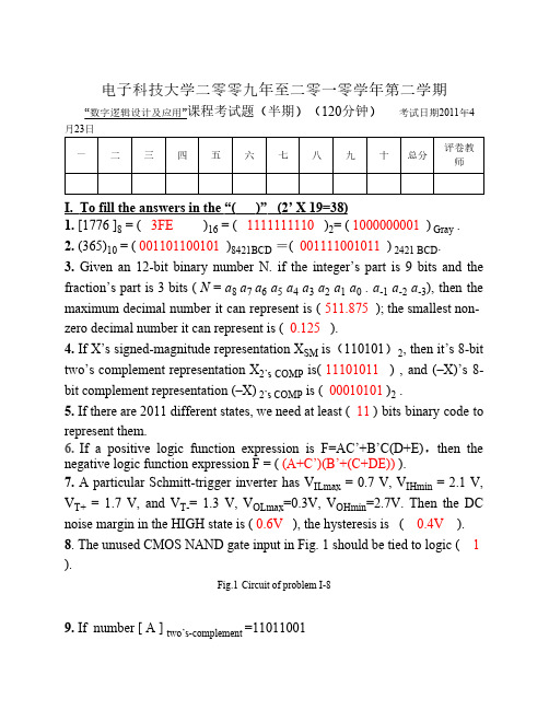
电子科技大学二零零九年至二零一零学年第二学期“数字逻辑设计及应用”课程考试题(半期)(120分钟)考试日期2011年4月23日一二三四五六七八九十总分评卷教师I. To fill the answers in the “( )” (2’ X 19=38)1. [1776 ]8 = ( 3FE )16 = ( 1111111110 )2= ( 1000000001 ) Gray .2. (365)10 = ( 001101100101 )8421BCD=( 001111001011 ) 2421 BCD.3.Given an 12-bit binary number N. if the integer’s part is 9 bits and the fraction’s part is 3 bits ( N = a8 a7 a6 a5 a4 a3 a2 a1 a0 . a-1 a-2 a-3), then the maximum decimal number it can represent is ( 511.875 ); the smallest non-zero decimal number it can represent is ( 0.125 ).4. If X’s signed-magnitude representation X SM is(110101)2, then it’s 8-bit two’s complement representation X2’s COMP is( 11101011 ) , and (–X)’s 8-bit complement representation (–X) 2’s COMP is ( 00010101 )2 .5. If there are 2011 different states, we need at least ( 11 ) bits binary code to represent them.6.If a positive logic function expression is F=AC’+B’C(D+E),then the negative logic function expression F = ( (A+C’)(B’+(C+DE)) ).7. A particular Schmitt-trigger inverter has V ILmax = 0.7 V, V IHmin = 2.1 V, V T+= 1.7 V, and V T-= 1.3 V, V OLmax=0.3V, V OHmin=2.7V. Then the DC noise margin in the HIGH state is ( 0.6V ), the hysteresis is ( 0.4V ). 8.The unused CMOS NAND gate input in Fig. 1 should be tied to logic ( 1 ).Fig.1Circuit of problem I-89. If number [ A ] two’s-complement =11011001and [ B] two’s-complement=10011101 , calculate[-A-B ]two’s-complement, [-A+B ]two’s-complement and indicate whether or not overflow occurs.[-A-B ] two’s-complement=[ 10001010 ], overflow: [ yes ][-A+B ] two’s-complement=[ 11000100 ], overflow: [ no ].10.The following logic diagram Fig.2 implements a function of 3-variable with a 74138. The logic function can be expressed as F (A,B,C) = ∑A,B,C ( 0,1,2 ).Fig.2 Circuit of problem I-10II. There is only one correct answer in the following questions.(3’ X 9 = 27)1. Which of the following Boolean equations is NOT correct? ( B )A) A+0=A B) A1 = AC) D)2. Suppose A2’s COMP =(1011),B2’s COMP =(1010),C2’s COMP =(0010). In the following equations, the most unlikely to produce overflow is( C )。
西安电子科技大学2011年811信号与系统考研真题+答案

2z2 ,则原序列 f (k ) 等于 z2 1
三、计算题(共 4 小题,共 43 分)
12 2 j 4 1、 (12 分)一线性时不变因果连续系统的频率响应函数为 H ( j ) 2 2 j 3
(1)求该系统的冲激响应 h(t ) ; (2)若系统输入 f (t ) e
西安电子科技大学 2011 年攻读硕士学位研究生入学考试试题
考试科目代码及名称:811 信号与系统、通信原理 第一部分:通信原理(总分 75 分)
第二部分:信号与系统(总分 75 分) 一、选择题(共 4 小题,每小题 4 分,共 16 分)
1、积分
4
sin(t 1) (2t 2)dt 等于 t 1
4 t
(t ) 时系统的全响应 y (t ) 5e t 7e2t 2e4t (t )
求系统的起始状态(又称 0 初始状态) y (0 ), y(0 ) 。 2、 (12 分)描述某线性时不变因果离散系统的差分方程为
6 y (k ) 5 y (k 1) y (k 2) 6 f (k ) 12 f (k 1)
4、 (7 分)图 2-3 为线性时不变离散系统的框图,图中方框 D 为单位延迟器。 (1)若状态变量 x1 , x2 , x3 如图中所标,试列写出该系统的状态方程与输出方程的矩 阵形式; (2)试列写该系统的输入输出差分方程。
4
f (k )
x1
1ቤተ መጻሕፍቲ ባይዱ
2
x2
3
5
x3 y (k )
6
2
2011 年《信号与系统》真题答案详解
西安电子科技大学《电路、信号与系统》真题2011年

西安电子科技大学《电路、信号与系统》真题2011年(总分:75.00,做题时间:90分钟)一、{{B}}{{/B}}(总题数:6,分数:24.00)1.T等于______。
∙ A.20s∙ B.40s∙ C.60s∙ D.120s(分数:4.00)A.B.C. √D.解析:[解析] [*],f(k)的周期T为T1、T2、T3的最小公倍数,即为60s。
2.-τδ"(τ)dτ等于______。
∙ A.δ(t)+u(t)∙ B.δ(t)+δ'(t)∙ C.δ'(t)+2δ(t)+u(t)∙ D.δ'(t)(分数:4.00)A.B.C. √D.解析:[解析] [*]3.卷积积分(t+1)u(t+1)*δ'(t-2)等于______。
∙ A.δ(t-1)∙ B.u(t-1)∙ C.δ(t-3)∙ D.u(t-3)(分数:4.00)A.B. √C.D.解析:[解析] 原式=tu(t)*δ'(t-1)=[tu(t)]'*δ(t-1)=u(t)*δ(t-1)=u(t-1)。
4.______。
∙ A.1∙ B.0.5π∙ C.π∙ D.2π(分数:4.00)A.B. √C.D.解析:[解析] 根据傅里叶变换定义式,有F(jω)=[*]f(t)e-jωt dt,则:[*]根据常用傅里叶变换,可知Sa(t)[*]F(jω)=πG2(ω)。
所以:[*]5.因果信号f(k)F(z)的收敛域为______。
∙ A.|z|>2∙ B.|z|>1∙ C.|z|<1∙ D.1<|z|<2(分数:4.00)A. √B.C.D.解析:[解析] 离散系统因果信号收敛域为|z|>a,非因果信号收敛域为|z|<b,因为F(z)=[*]的极点为p1=-1,P2=2。
所以,当|z|<1时,则f(k)为非因果信号;当1<|z|<2时,则f(k)为因果信号及非因果信号两部分;当|z|>2时,则f(k)为因果信号。
电子科大信号与系统习题解答1

信号与系统习题解答11.1 用代数式表达下列复数:已知形式为θj re ,要求表达形式为jy x +,采用公式:θcos r x =,θsin r y =。
解: 2121-=πj e 2121-=-πj ej e j =2π j e j -=-2πj ej=25πj ej+=124π j ej+=1249πj ej -=-1249π j ej-=-124π1.2 用极式表达下列复数:已知形式为jy x +,要求表达形式为θj re ,采用公式:22y x r +=,()πθπθ≤<-=-xytg 1。
解:055j e = πj e 22=- 233πjej -=-()2242221ππjj e e j --=⎪⎪⎭⎫ ⎝⎛=- ()442221πππjjje eej j =⋅=--2442211πππjjje ee jj ==-+-1234223122πππjj je e ej j -==++1.54 (a )证明表达式 ⎪⎩⎪⎨⎧≠--==∑-=111110αααααN N n nN证: 因为 1=α 时,1=n α (n 为任意值时)所以,1=α 时,N N n n =∑-=10α因为 ()()NN ααααα-=++++--1 (111)2所以,当1≠α时,()ααααα--=++++-11 (11)2NN 原式得证。
(b) 证明:1<α时,αα-=∑∞=110n n 证:因为 1<α时,0lim ==∞→NN α所以:αααα-=--=∞→∞=∑1111lim 0N N n n(c )证明:1<α时,()21ααα-=∑∞=n nn 证:令()αααf n n=-=∑∞=11为α的连续函数对上式进行微分运算可得:()()2111αααα-==∑∞=-n n n d df 同时乘以α就可以得到:()21αααααα-==∑∞=n nn d df (d )当1<α时,计算?=∑∞=kn nα解: 因为∑∑∑∞=-=∞=+=kn nk n n n n ααα100所以:αααααααα-=----=-=∑∑∑-=∞=∞=1111110kk k n nn nk n n1.55 计算下列和式,采用代数式表达。
电子科大考研真题:836信号与系统和数字电路
输出 RCO
0 0 0 0 0 0 0 0 0 1
图 2-3
第6页 共7页
三:设计题(二小题共 25 分)(设计题可以不画具体电路图,但必须有详细且明确的连接 关系表达,如逻辑函数表达;器件管脚说明,信号-管脚连接表等。) 1)(10 分)设计一个实现 Z=2.5·Y 乘法运算的组合电路,其中 Y 是输入,为 4_bit 二进 制码字;Z 为二进制输出。(电路实现结构、器件自选,必须说明设计思路。) 2)(15 分)试用 D 触发器和必要的逻辑门设计一个时钟同步状态机电路。电路功能要求: 在电路复位(低电平复位)有效后,每输入 5 个时钟脉冲时,在第 3 个和第 4 个时钟脉冲处, 输出端 Z 都有一个脉冲输出(波形如图 3-2 所示)。由于后续电路对输出信号 Z 的脉冲边沿 有要求,请在设计中考虑器件延时对输出波形的影响;要求能自启动。(电路结构、器件自 选,必须说明设计思路。)
二、(10分)已知 LTI(线性时不变)连续时间系统冲激响应为 h0 (t) ,当输入是 f0 (t) 时,
响应为 y0 (t) 。如果另一 LTI 连续时间系统冲激响应 h(t) 和输入信号 f (t) 分别表示如下,
并设其响应为 y (t) 。用卷积的概念和性质求系统的响应 y (t) (用 y0 (t) 表示)。(请给出推
j sin(5πt)
h 2(t)
y3 (t)
f(t)
h 1(t)
y1(t)
y(t)
图 2 (a)
F(ω) 1
−2π
0
2π ω
图 2 (b) 图 2、第4题图
第3页 共7页
五、(16 分)求解下列问题:
∞
∑ (1)信号 m(t) = δ (t − kT ) ,T > 0 ,是否周期信号,若是,周期是多少? k =0 ∞
电子科大信号与系统期中考试试卷及答案11-12学年
………密………封………线………以………内………答………题………无………效……电子科技大学二零 一 一 至二零 一 二 学年第 一 学期期 中 考试SIGNALS AND SYSTEMS 课程考试题 卷 ( 120 分钟) 考试形式: 闭卷 考试日期 20 11 年 月 日课程成绩构成:平时 10 分, 期中 20 分, 实验 10 分, 期末 60 分1(56points).Each of the following questions may have one or two right answers, justify your answers and write it in the blank. (1)()cos 221πδ+∞-∞-=⎰t t dt ( d ).(a) 1 (b) -1 (c) 0.5 (d) -0.5(2) The fundamental period of the signal []23cos sin 32ππ⎡⎤⎡⎤=-⎢⎥⎢⎥⎣⎦⎣⎦x n n n is ( a ). (a) 12N = (b) 6N = (c) 8N = (d) 24N = (3) Let ()1tx t e -= and ()()()14k x t x t t k δ+∞=-∞=*-∑. The Fourier series coefficients of ()x t may be ( a ).(a) {} and Im 0-==k k k a a a (b) {} and Im 0-=-=k k k a a a (c) {} and Re 0-==k k k a a a (d) {} and Re 0k k k a a a -=-=(4) Consider an LTI system with unit impulse response ()h t illustrated in Figure 1, if the input is ()()d t x t dtδ=, the output () 0.5t y t =- is( b ).(a) -1 (b) 1 (c) -0.5 (d) 0.5(5) The convolution integral ()222t te e u t -*=( c ).(a) 2 (b)214te (c)212te (d)()212te u t(6) Which of the following systems is an linear system ( a ). In each example, []y n denotes the system output and []x n is the systeminput.(a) [][][]cos y n n x n = (b) [][]{}cos 3y n x n = (c) [][]()ln y n x n = (d) [][]2y n x n =(7) Which of the following systems are causal and stable system ( ad ). In each example, ()h t denotes the impulse response of thefollowing systems.(a) ()()()13h t t t δδ=-+- (b) ()()()0.5cos 2t h t t e u t =- (c) ()()()13h t t t δδ=+++ (d) ()()()cos 2t h t t e u t -=-(8) Determine the following signals which have finite total energy ( bc ). (a) []()[]1x n n u n =+ (b) ()()23tx t eu t -=+(c) []()[]1cos /32nx n n u n π⎛⎫= ⎪⎝⎭(d) () , tx t e t =-∞<<+∞tFigure 1………密………封………线………以………内………答………题………无………效……(9) Consider a continuous-time LTI system whose frequency response is ()()sin /2Hj ωωω=. If we know the output ()y t to some periodicinput signals are ()0y t =. The fundamental period of the input signal may be ( ac ). (a) 1T = (b) 2T = (c) 0.5T = (d) 3T =2(12points). A continuous-time signal ()32-+x t is illustrated in Figure 2.(a) Determine the signal ()x t . (b) Sketch and label carefully ()x t .3(10 points).Consider an LTI system whose response to the signal ()t x 1 in Figure 3 is the signal ()t y 1 illustrated in Figure 4. Determine the response of the system to the input ()t x 2 depicted in Figure 5 .4(12 points). Consider a continuous-time LTI system whose frequency response ()H j ω is illustrated in Figure 6. If the input signal()1cos 3sin 6ππ=++x t t t , determine the output of the system.12Figure 3ωFigure 6tFigure 2………密………封………线………以………内………答………题………无………效……14(10points). Consider an LTI system whose input []x n and unit impulse response []h n are given by []{}1,0,1,1,0,1x n n =-=-,[]{}2,1,3,2,2,3,4,5h n n ==. Determine the output [][][]n h n x n y *= of this system.《信号与系统》半期考试评分标准说明1.填空题(56分)⑴. (d) ⑵ (a) ⑶ (a) ⑷ (b) ⑸ (c) ⑹ (a) ⑺ (ad) ⑻ (bc) ⑼ (ac) ⑽ (ab) 本部分评分规则:1) 选择题共14个正确答案,1-6题为单选,7-10题为双选; 2) 若只填写了1个答案,正确得4分,错误得0分;3) 若填写了2个答案,2个正确得8分,1个正确、1个错误得4分,2个错误得0分;4) 若填写了3个答案,2个正确、1个错误得4分,1个正确、2个错误得2分,3个错误得0分; 5) 若填写了4个答案,得0分。
电子科大《信号与系统》考卷汇总
高通滤波器
允许高频信号通过,抑制低频信号,用于提 取高频成分。
带通滤波器
允许某一频段的信号通过,抑制其他频段的 信号,用于提取特定频率范围的信号。
陷波滤波器
抑制特定频率的信号,用于消除特定频率的 干扰。
05
CATALOGUE
系统的频域分析
系统的频域响应
频域响应的定义
系统的频域响应是指在频域中描述系统对输入信号的响应特性。
实现信号处理算法的工具
实现信号处理算法需要使用专业的工具和软件,如MATLAB、Python等。这些工具提供了丰富的函数库 和工具箱,方便用户进行信号处理和分析。
系统设计中的信号处理技术
系统设计中的信号处 理需求
在系统设计中,信号处理技术是 必不可少的。系统中的信号可能 受到噪声、干扰和其他因素的影 响,导致信号质量下降。因此, 需要进行信号处理以提取有用信 息,提高信号质量。
过程。
02
调制解调技术的分类
调制解调技术可以分为模拟调制和数字调制两大类,模拟调制包括调频
、调相和调幅等,数字调制包括振幅键控、频率键控和相位键控等。
03
调制解调技术的应用
调制解调技术广泛应用于通信、雷达、声呐和遥控等领域,是实现信号
传输和处理的关键技术之一。
06
CATALOGUE
信号与系统的综合应用
信号的时移
将信号在时间轴上移动一定的时间,可以得到一 个新的信号。
信号的展缩
将信号的幅度进行放大或缩小,可以得到一个新 的信号。
信号的反转
将信号在时间轴上进行翻转,可以得到一个新的 信号。
03
CATALOGUE
系统的时域分析
系统的时域响应
瞬态响应
西安电子科技大学821电路、信号与系统2011年考研专业课真题答案
则Z
=
������̇ ������̇
=
3
+
������4
ZL = Z∗ = 3 − ������4
4.C 解
运用阻抗匹配求解,等效电路如下:
Is
+
4
UL -
12
由 I(s) = 16∠0 ⇒ UL = 48∠0
2011 电路
所以U̇ = −24∠0
5.B 解 运用相量图,设电流表 A1 为 0 相位,则 A2 超前π,
6 2+4������
3
⇒
U̇ ������
=
2(1+2������) 1+������
所以İ������1
=
������̇ ������ 2+4������
=
1 1+������
⇒
������1
=
√2 cos (2������
2
−
������)
4
所以IL1(0−)
=
1 2
������
所以U(∞) = 6V
+ 4I -
10A
I5
1
R
I2������ = 50 6(10 + I) + 4I + RI = 0 联立得R = 50或R = 2 8.电路耦合等效电路如图,
+ Us -M
+
L1-M
UL
-
L2-M
U2即为(L1 − M)上电压,由L1 − ������ = ������可知
U2
=
1 2
������������
=
������̇ ������ ������