STM8教程-第十六章 CCO 时钟输出
STM8学习笔记——时钟和GPIO

STM8学习笔记——时钟和GPIO说起STM8 的时钟,那还真是个杯具,用HSI 没问题,切换到HSE 也没问题,就是切LSI 怎么都不行,然后百思不得其解人,然后上论坛求教,才知道还有个选项字节(OPTION BYTE),数据手册上有这么一段描述:选项字节包括芯片硬件特性的配置和存储器的保护信息,这些字节保存在存储器中一个专用的块内。
除了ROP(读出保护)字节,每个选项字节必须被保存两次,一个是通常的格式(OPTx)和一个用来备份的互补格式(NOPTx)要使用内部低速RC 必须将LSI_EN 置1,就是这个地方让我纠结了半天,然后用IAR 将其置1,方法是:进入调试模式,在上面有个ST-LINK,点击,看到OPTION BYTE,左键点进去,右键单击上面的选项,就可更改了,然后全速运行,就写进去了。
STM8 的时钟分为HSI,HSE,LSI,最常用的是HSI,STMS105S4 内置的是16M 的RC,叫fhsi。
它可以分频输出为fhsidiv=fhsi/hsidiv,如果选择其为主时钟源,那么主时钟fmaster=fhsidiv。
CPU 时钟fcpu=fmaster/cpudiv。
可以通过外设时钟门控寄存器CLK_PCKENR1 和CLK_PCKENR2 选择是否与某个外设连接。
好了上个切换内部时钟的源代码,测试通过void CLK_Init(void){ //切换到内部LSI(!!!需要修改选项字节的LSI_EN 为1)CLK_ICKR|=0x08;//开启内部低速RC 震荡while(CLK_ICKR&0x10==0); //LSI 准备就绪CLK_SWR=0xd2; while(CLK_SWCR&0x08==0); //等待目标时钟源就绪CLK_SWCR|=0x02; //CPU 分频设置CLK_CKDIVR=0;//内部RC 输出。
stm8 cosmic基本教程

...
MCD Application
16
关于flash 操作(IAP)
#pragma section (FLASH_CODE) void FlashWrite(void) { ... } void FlashErase(void) { ... } //set back code section to default placement #pragma section ()
From On-chip Peripherals
M外部中断
Filtering Edge Detection Trigger selection Capture Selection Dividing
MCD Application
21
采用输入捕获方式获得外部中断
MCD Application
9
Memory Models>64k (FLASH>32K)
Stack Short (mods) 全局变量默认为是短寻址方式( 全局变量默认为是短寻址方式(位置存放在 小于256的空间 0page) 在变量前 @near 或用指针方式长寻址 Stack Long (modsl) 全局变量默认为是长寻址方式( 全局变量默认为是长寻址方式(位置存放在 大于256的空间) 的空间) 在变量前 @tiny 或用指针方式长寻址 一般来讲,变量放在<256的空间内效率更高
MCD Application
8
Memory Models<64k(FLASH<32K)
Stack Short (mods0) 全局变量默认为是短寻址方式 ( @tiny 存放 在zero page ,8位地址) 位地址) 超出zero page范围须的变量须用 @near定义 Stack Long (modsl0) 全局变量默认为是长寻址方式( 全局变量默认为是长寻址方式( @near 存放 在0x100开始的地址16位空间 ) zero page内定义变量需要加 @tiny 强制定义 一般来讲,变量放在zero page的空间内效率 更高
STM8S系统时钟应用(IAR)

STM8S系统时钟应用(IAR)
STM8 上电运行时默认使用内部16M 的RC 振荡器经8 分频后的2M 时钟
频率作为系统时钟。
程序开始运行后可以通过设置相关寄存器来修改主时钟源,可以选择外部晶振作为主时钟源和CPU 时钟分频。
那么这里就选择比较简单
的操作,修改内部RC 时钟预分频器获得8M 系统时钟。
增加内部RC 时钟预
分频后的代码如下:
#i nclude #define LED1_FLASHPD_ODR_ODR3 =!PD_ODR_ODR3// LED 闪灯指示void delay(unsigned int count){while(count--);}void CLK_init(void){ CLK_CKDIVR = 0x08; // 16M 内部RC 经2 分频后系统时钟为8M}void GPIO_init(void){PD_DDR = 0x08;// 配置PD 端口的方向寄存器PD3 输出PD_CR1 = 0x08;// 设置PD3 为推挽输出}void init_devices(void){CLK_init(); GPIO_init();}void main( void ){init_devices();while(1){ delay(50000); LED1_FLASH;}}编译后运行一下看看,LED1 是不是闪得更快了
tips:感谢大家的阅读,本文由我司收集整编。
仅供参阅!。
STM8单片机时钟应用

位2 0 0 0 0 1 1 1 1
位1 0 0 1 1 0 0 1 1 0 1 0 12 4 8 16 32 64 128
例如:假设我们使用内部的高速 RC 振荡器,其频率为 16MHZ ,当我们设置 C PU 时钟的分频系数为 2 时(即位[2:0] 为:0,0,1),得到 CPU 时钟=主时钟/ 2=8MHZ 。
时钟
在有些单片机的应用系统中,并不需要 CPU 运行在多高的频率。在低频率下运 行,芯片的功耗会大大下降。所以在这里我们需要了解下时钟控制,其目的就在 于使用户获得最好性能的同时,也能保证消耗的功率最低。 一、主时钟源介绍 本开发板有 3 种主时钟源: ● 24MHz 高速外部晶体振荡器(HSE) ● 16MHz 高速内部 RC 振荡器(HSI ) ● 128KHz 低速内部 RC(LSI) 用户可独立的管理各个时钟源,并将它们分配到 CPU 或各个外设。主时钟和 C PU 时钟均带有预分频器。 注:单片机复位后,首先采用的是内部的高速 RC 振荡器,且分频系数为 8,因 此 CPU 的上电运行的时钟频率为 2MHZ。 二、切换主时钟源 切换时钟源,主要涉及到的寄存器有: ● 主时钟切换寄存器 CLK_SWR ● 切换控制寄存器 CLK_SWCR 主时钟切换寄存器的复位值为 0xe1 ,表示切换到内部的高速 RC 振荡器上。 当往该寄存器写入 0xb4 时,表示切换到外部的高速晶体振荡器上。 在实际切换过程中按照如下步骤操作即可 1. 应该先将切换控制寄存器(CLK_SWCR)中的 SWEN(第 1 位)设置成 1, 使能切换机制。 2. 然后设置主时钟切换寄存器(CLK_SWR)的值,用以选择目标时钟源。 3. 最后要判断切换控制寄存器中的 SWIF 标志是否切换成功。 三、修改 CPU 时钟 实现这一功能,主要涉及到时钟分频寄存器(CLK_CKDIVR)。 CPU 时钟由主时钟分频而来,分频因子由时钟分频寄存器(CLK_CKDIVR)中 的位[2:0] 决定,共 7 个分频因子可供选择。 对应关系如下:
stm8教程
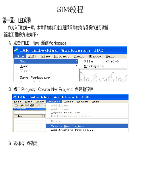
STM8教程第一章:LED实验作为入门的第一章,本章将如何新建工程跟简单的寄存器操作进行讲解新建工程的方法如下:1、点击FILE,New,新建Workspace2、点击Project,Create New Project,创建新项目3、选择C,点确定4、弹出另存为对话框,选择project保存的路径,并输入project的名字5、创建工程后的界面如下图所示6、保存Workspace,指定要保存的路径,并输入Workspace的名字7、工程选项的有关配置:在Workspace窗口,选中project名,右键选择Options或者在工具菜单栏选择project->Options8、在Category中选择General Options,右边Target的Device选择设备型号,由于我们采用的是stm8s105k6t6,故选择相应的型号即可,其他的按默认设置9、左边选择C/C++ Compiler,在C/C++ Compiler -> Preprocessor中的Additional栏中是设置*.h文件所在的位置,填入如下10、左边选择Output Converter,在Output Converter -> Output中勾选Generate在Output file下的栏中输入生成hex的文件名好了,工程建好了,接下来开始给力的时候咯,迫不及待吧,哈哈,别急纳在这里讲几句唠叨的,在用某个单片机之前,先要看看数据手册对它的简单描述,个人觉得这点很重要,在往后的学习中就会发现,并养成这个习惯的唠叨部分:查看stm8s105的数据手册,大概浏览时钟跟引脚的一些描述如上大概知道这个芯片上电后的时钟默认为2MHz,并且可以配置不同的时候源,大概先了解这些先,多了就不好受了。
关于这个表,可以大概看出引脚作为输出时,可以配置不同的速率。
输出输入的的模式也有好几种。
哎呀,啥时候才实际操刀啊,好过过手隐啊好吧。
大展拳脚:板子的LED连接图:实验内容:先点亮LED,然后再让它一闪一闪这是一个配置引脚的数据方向寄存器,为输入或者输出。
stm8l中文参考手册(下)
手动开关手动开关没有自动切换为直接的但它提供给用户的切换事件时间的精确控制。
参照图20中的流程图。
1。
写使用系统时钟开关选择目标时钟源的8位值寄存器(clk_swr)。
然后swbsy位是由硬件,和目标源振荡器开始。
古老的时钟源继续驱动CPU和外设。
2。
该软件具有等到目标时钟源准备(稳定的)。
这是在clk_swcr寄存器和快捷旗由中断如果swien位设置显示。
3。
最终软件的作用是设置,在所选择的时间,在clk_swcr的赛文点寄存器来执行开关。
在手动和自动切换模式,旧的系统时钟源不会自动关闭的情况下是由其他模块(LSI混凝土可用于例如独立的看门狗驱动)。
时钟源可以关机使用在内部时钟寄存器的位(clk_ickcr)和外部时钟寄存器(clk_eckcr)。
如果时钟开关不因任何原因的工作,软件可以通过清除swbsy 标志复位电流开关操作。
这将恢复clk_swr注册到其以前的内容(旧的系统时钟)。
注意:在清理swbsy标志具有复位时钟主开关的程序,应用程序必须等到后产生新的主时钟切换请求之前有一段至少两个时钟周期。
9.7周门控时钟(PCG)外周时钟门控(PCG)模式选择性地启用或禁用系统时钟(SYSCLK)连接到外围设备在运行或慢速模式的任何时间来优化功耗。
设备复位后,所有的外设时钟被禁用。
唯一的一点是在复位状态是默认启用pcken27因为它用于启动。
软件已被正确地写入关掉ROM Bootloader执行后的时钟。
您可以启用时钟的任何外围设置在clk_pckenrx周围门控时钟寄存器的相应pcken点。
●使周围,首先使在clk_pckenr相应的pcken点寄存器然后设置使点周围的外围控制寄存器。
●禁用适当的外围,先禁用在周边的适当位控制寄存器,然后停止相应的时钟。
注:蜂鸣器,RTC和液晶显示器是由不同的SYSCLK特定的时钟,使他们继续运行,即使时钟门控的外设寄存器是断言。
9.8时钟安全系统(CSS)9.8.1时钟安全系统对HSE时钟安全系统(CSS)监控HSE晶体时钟源故障时安全作为系统时钟。
STM8L中文参考手册-2
手动开关手动开关没有自动切换为直接的但它提供给用户的切换事件时间的精确控制。
参照图20中的流程图。
1。
写使用系统时钟开关选择目标时钟源的8位值寄存器(clk_swr)。
然后swbsy位是由硬件,和目标源振荡器开始。
古老的时钟源继续驱动CPU和外设。
2。
该软件具有等到目标时钟源准备(稳定的)。
这是在clk_swcr寄存器和快捷旗由中断如果swien位设置显示。
3。
最终软件的作用是设置,在所选择的时间,在clk_swcr的赛文点寄存器来执行开关。
在手动和自动切换模式,旧的系统时钟源不会自动关闭的情况下是由其他模块(LSI混凝土可用于例如独立的看门狗驱动)。
时钟源可以关机使用在内部时钟寄存器的位(clk_ickcr)和外部时钟寄存器(clk_eckcr)。
如果时钟开关不因任何原因的工作,软件可以通过清除swbsy 标志复位电流开关操作。
这将恢复clk_swr注册到其以前的内容(旧的系统时钟)。
注意:在清理swbsy标志具有复位时钟主开关的程序,应用程序必须等到后产生新的主时钟切换请求之前有一段至少两个时钟周期。
9.7周门控时钟(PCG)外周时钟门控(PCG)模式选择性地启用或禁用系统时钟(SYSCLK)连接到外围设备在运行或慢速模式的任何时间来优化功耗。
设备复位后,所有的外设时钟被禁用。
唯一的一点是在复位状态是默认启用pcken27因为它用于启动。
软件已被正确地写入关掉ROM Bootloader执行后的时钟。
您可以启用时钟的任何外围设置在clk_pckenrx周围门控时钟寄存器的相应pcken点。
●使周围,首先使在clk_pckenr相应的pcken点寄存器然后设置使点周围的外围控制寄存器。
●禁用适当的外围,先禁用在周边的适当位控制寄存器,然后停止相应的时钟。
注:蜂鸣器,RTC和液晶显示器是由不同的SYSCLK特定的时钟,使他们继续运行,即使时钟门控的外设寄存器是断言。
9.8时钟安全系统(CSS)9.8.1时钟安全系统对HSE时钟安全系统(CSS)监控HSE晶体时钟源故障时安全作为系统时钟。
STM8-时钟,中断,TIM系统-推荐下载
说实话我能够使用的单片机不多,我总是以为无论什么单片机都能开发出好的产品。
前些年用51,总是向各位大大学习,无休止的索取,在网上狂览一通。
心里感激的同时也想奉献一些,可是我会什么?后来使用avr(公司要求)还是向大大们学习,我又想奉献,可是我会什么?我会的大大们都写了,我不会的大大们也写了。
一个星期前花项目经费买了阿莫的kit三合一板,最近几天闲了下来,便动手调试一下。
算是有点心得,我又想奉献,可是我会什么?我只是想和大大们交流一下,哪怕是对的或者是错的,大大们满足我的一点心愿吧。
唠叨了这么多,现在开始吧。
配置:stvd ,cosmic我学单片机开门三砖总是要砸的。
第一砖:电源系统,这没什么好说的,只是它是stm8工作的基础总是要提一下第二砖:时钟系统,这等下再说。
第三砖:复位系统,stm8只需要一只104电容从reset脚到地就可以了。
现在说说时钟系统,学习单片机无论8位的还是32位的,都要从时钟开始,下面是我一开始的时钟切换程序。
1 CLK_ECKR |=0X1; //开启外部时钟2 while(!(CLK_ECKR&0X2)); //等待外部时钟rdy3 CLK_CKDIVR &= 0XF8; //CPU无分频4 CLK_SWR = 0XB4; //选择外部时钟5 CLK_SWCR |=0X2; //使能外部时钟上面的代码看起来没什么问题,可在调试过程中出现了有时能切换,有时有不能的情况,后来发现只要在第5行设上断点就能切换,我就想是不是得让cpu等一下,我又仔细的翻看下rm0016的时钟部分,发现得等待CLK_SWCR的标志位置位才能切换。
就变成了下面的代码CLK_ECKR |=0X1; //开启外部时钟while(!(CLK_ECKR&0X2)); //等待外部时钟rdyCLK_CKDIVR &= 0XF8; //CPU无分频CLK_SWR = 0XB4; //选择外部时钟while(!(CLK_SWCR&0X8)); //这里要等CLK_SWCR |=0X2; //使能外部时钟现在一切ok,是不是觉得看东西要仔细一下~~。
STM8时钟配置笔记
//-----------------------------------------------------------------------------------------
void CLK_DeInit(void);
参数:
NewState: 新的状态值
DISABLE 禁用
ENABLE 启用
返回值:无
//-----------------------------------------------------------------------------------------
DISABLE 禁用
ENABLE 启用
返回值:无
如果为了能快速从活跃停机模式中唤醒,进入活跃停机前则调用CLK_SlowActiveHaltWakeUpCmd(ENABLE);但功耗较大。
如果进入活跃停机模式前没有调用CLK_SlowActiveHaltWakeUpCmd(ENABLE);或调用了CLK_SlowActiveHaltWakeUpCmd(DISABLE);即默认的情况下
CLK_PERIPHERAL_UART2
CLK_PERIPHERAL_UART3
CLK_PERIPHERAL_TIMER6
CLK_PERIPHERAL_TIMER4
CLK_PERIPHERAL_TIMER5
CLK_PERIPHERAL_TIMER2
恢复相关的时钟寄存器到默认值
参数:无
返回值:无
注意:
当要复位CCOR寄存器时,如果CCOEN位被置位,则需要先复位CCOEN位,然后再复位CCOSEL位,复位CCOEN位和复位CCOSEL位的操作必须连续。
STM8 Debugger手册说明书
STM8 Debugger Release 09.2023TRACE32 Online HelpTRACE32 DirectoryTRACE32 IndexTRACE32 Documents ......................................................................................................................ICD In-Circuit Debugger ................................................................................................................Processor Architecture Manuals ..............................................................................................STM8 .........................................................................................................................................STM8 Debugger (1)Warning (4)Introduction (5)Brief Overview of Documents for New Users5 Demo and Start-up Script5Configuration (6)System Overview6Quick Start (7)Troubleshooting (9)FAQ (10)STM8 specific SYStem Settings (11)SYStem.CPU Select the used CPU11 SYStem.MemAccess Real-time memory access (non-intrusive)11 SYStem.Mode Establish the communication with the target12 SYStem.LOCK Lock and tristate the debug port12 SYStem.Option.IMASKASM Disable interrupts while single stepping13 SYStem.Option.IMASKHLL Disable interrupts while HLL single stepping13CPU specific TrOnchip Commands (14)Breakpoints (15)Software breakpoints15 On-chip breakpoints for instructions15 On-chip breakpoints for data15Memory Classes (16)Target Adaption (17)Connector Type and Pinout17Version 10-Oct-2023WarningWARNING:T o prevent debugger and target from damage it is recommended to connect ordisconnect the debug cable only while the target power is OFF.Recommendation for the software start:1.Disconnect the debug cable from the target while the target power isoff.2.Connect the host system, the TRACE32 hardware and the debugcable.3.Power ON the TRACE32 hardware.4.Start the TRACE32 software to load the debugger firmware.5.Connect the debug cable to the target.6.Switch the target power ON.7.Configure your debugger e.g. via a start-up script.Power down:1.Switch off the target power.2.Disconnect the debug cable from the target.3.Close the TRACE32 software.4.Power OFF the TRACE32 hardware.IntroductionThis document serves as a guideline for debugging STM8 MCUs and describes all MCU-specific TRACE32 settings and features.Please keep in mind that only the Processor Architecture Manual (the document you are reading at the moment) is CPU specific, while all other parts of the online help are generic for all CPUs supported by Lauterbach. So if there are questions related to the CPU, the Processor Architecture Manual should be your first choice.Brief Overview of Documents for New UsersArchitecture-independent information:•“Training Basic Debugging” (training_debugger.pdf): Get familiar with the basic features of a TRACE32 debugger.•“T32Start” (app_t32start.pdf): T32Start assists you in starting TRACE32 PowerView instances for different configurations of the debugger. T32Start is only available for Windows.•“General Commands” (general_ref_<x>.pdf): Alphabetic list of debug commands.Architecture-specific information:•“Processor Architecture Manuals”: These manuals describe commands that are specific for the processor architecture supported by your Debug Cable. T o access the manual for your processorarchitecture, proceed as follows:-Choose Help menu > Processor Architecture Manual.•“OS Awareness Manuals” (rtos_<os>.pdf): TRACE32 PowerView can be extended for operating system-aware debugging. The appropriate OS Awareness manual informs you how to enable theOS-aware debugging.Demo and Start-up ScriptLauterbach provides ready-to-run start-up scripts for known hardware that is based on STM8.To search for PRACTICE scripts, do one of the following in TRACE32 PowerView:•Type at the command line: WELCOME.SCRIPTS•or choose File menu > Search for Script.Y ou can now search the demo folder and its subdirectories for PRACTICE start-up scripts(*.cmm) and other demo software.Y ou can also manually navigate in the ~~/demo/stm8/ subfolder of the system directory of TRACE32.The on-chip FLASH and the EEProm memory can be programmed via the stm8.cmm script: CD.DO ~~/demo/stm8/flash/stm8.cmmPlease be aware that you should check the Flash and EEProm size specified for your MCU in the stm8.cmm before executing this script.ConfigurationSystem OverviewExample configuration for an STM8 debugger.Quick StartStarting up the debugger is done as follows:1.Select the device prompt B (BDM debugger) and reset TRACE32.B::RESetThe device prompt B:: is normally already selected in the TRACE32 command line. If this is not thecase, enter B:: to set the correct device prompt. The RESet command is only necessary if you donot start directly after booting the TRACE32 development tool.2.Specify the CPU specific settings.SYStem.CPU STM8S005K6This command selects the CPU type.rm the debugger about the cashable address range (FLASH/EEPROM)..MAP.UpdateOnce p:0x8000--0xffffThis is important to speed up the TRACE32 PowerView GUI responsiveness. The specified addressrange will be accessed only once after a break, thus avoiding unnecessary memory accesses.4.Reset the target and enter debug mode.SYStem.Mode UpThis command resets the CPU on the target, enables On-Chip-Debug Mode and issues a breakpointright after the reset interrupt routine.The CPU stops executing any instruction, and the user is able todownload and test the code. After this command is executed, it is possible to access memory andregisters.5.Load the program into the flash.A typical start sequence of the STM8 is shown below. This sequence can be written to a PRACTICE script file (*.cmm, ASCII format) and executed with the command DO <file>.*) These commands open windows on the screen. The window position can be specified with the WinPOS command.DO ~~/demo/stm8/flash/stm8.cmmB::; Select the ICD device prompt RESet; Reset the TRACE32 softwareMAP.UpdateOnce p:0x8000--0xffff ; Specify the address range for caching WinCLEAR ; Clear all windowsSYStem.Up; Reset the target and enter debug mode DO~~/demo/stm8/flash/stm8.cmm ; Load the target application into ; the FlashPER.view ; Show clearly arranged peripherals ; in window *)List.Mix; Open source code window *)Register.view /SpotLight ; Open register window *)Frame.view /Locals /Caller ; Open the stack frame with ; local variables *)Var.Watch %SpotLight flags ast ; Open watch window for variables *)Break.Set 0x1000 /Program; Set software breakpoint to address ; 1000 (address 1000 is within RAM ; address range)Break.Set 0x101000 /Program; Set on-chip breakpoint; to address 101000 (address 101000 is ; within Flash address range)TroubleshootingT ypically the SYStem.Up command is the first command of a debug session where communication with the target is required. If you receive error messages like “debug port fail” or “debug port time out” while executing this command, this may have the reasons below. “target processor in reset” is just a follow-up error message.•Open the AREA.view window to display all error messages.•If the target has no power or the debug cable is not connected to the target, this results in the error message “target power fail”.•Did you select the correct core type with SYStem.CPU <cpu>?•There is an issue with the SWD interface. Maybe there is the need to set jumpers on the target to connect the correct signals to the SWD connector.•The target is in an unrecoverable state. Re-power your target and try again.•The core is kept in reset.•There is a watchdog which needs to be deactivated.Error Message EventReason Target power fail SYStem.Mode.Up See below.Target processor in resetSYStem.DownSee below.Target is not connected or the SWD Interface is returning an error.SYStem.Mode.Up SYStem.Mode.GoThe debugger expects to receive a confirmation for each command sent to the target. An error occurs in case the confirmation is not received.The number of<number> accessed bytes in memory is not a multiple of the access <size> bytes.No special eventInternal error, please consult your Lauterbach representative.Memory <address> is not aligned to access <size>.No special eventInternal error, please consult your Lauterbach representative.Invalid memory access size: <size> bytes (@ <address>)No special eventInternal error, please consult your Lauterbach representative.Memory access timeout: Reading from <address>No special eventCorrupted JTAG connection. Check JTAG hardware and settings.FAQPlease refer to https:///kb.STM8 specific SYStem SettingsSYStem.CPUSelect the used CPUDefault: STM8xxx.Selects the processor type. All of the STM8 MCU cores with SWD Interface are supported.SYStem.MemAccessReal-time memory access (non-intrusive)Default: Denied. Format:SYStem.CPU <cpu><cpu>:STM8S005K6 | STM8S003K3 | STM8S001J3 | …Format:SYStem.MemAccess Enable | Denied | StopAndGoEnableCPU (deprecated)This option is not available at the moment.Denied Real-time memory access during program execution to target is disabled.StopAndGoTemporarily halts the core(s) to perform the memory access. Each stop takes some time depending on the speed of the JT AG port, the number of the assigned cores, and the operations that should be performed.For more information, see below.SYStem.ModeEstablish the communication with the targetDefault: Down. SYStem.LOCKLock and tristate the debug portDefault: OFF .If the system is locked, no access to the debug port will be performed by the debugger. While locked, the debug connector of the debugger is tristated. The main intention of the SYStem.LOCK command is to give debug access to another tool.Format:SYStem.Mode <mode>SYStem.Down (alias for SYStem.Mode Down)SYStem.Up (alias for SYStem.Mode Up)<mode>:Down Go UpNoDebugDown Disables the debugger. The state of the CPU remains unchanged. Go Resets the target and starts execution.Up Resets the target and stops the CPU at the reset vector.NoDebugThe debug adapter gets tristated.The state of the CPU remains unchanged. Debug mode is not active.In this mode the target behaves as if the debugger is not connected.Attach StandByNot available.Format:SYStem.LOCK [ON | OFF ]SYStem.Option.IMASKASM Disable interrupts while single steppingFormat:SYStem.Option.IMASKASM [ON | OFF]Default: OFF.If enabled, the interrupt enable flag of the EFLAGS register will be cleared during assembler single-step operations. After the single step, the interrupt enable flag is restored to the value it had before the step. It is turned on to make sure that no interrupt routine is serviced between Break and Go states. SYStem.Option.IMASKHLL Disable interrupts while HLL single steppingFormat:SYStem.Option.IMASKHLL [ON | OFF]Default: OFF.If enabled, the interrupt enable flag of the EFLAGS register will be cleared during HLL single-stepoperations. After the single step, the interrupt enable flag is restored to the value it had before the step.CPU specific TrOnchip CommandsThe TrOnchip command group is not available for the STM8 debugger.BreakpointsSoftware breakpointsThe Microchip STM8 architecture does not support software breakpoints.On-chip breakpoints for instructionsThe STM8 MCUs support a total of two on-chip breakpoint registers which can be used as programbreakpoints to stop and debug the program which executes always in the Flash.On-chip breakpoints for dataData breakpoints are used to analyze the read and write accesses to global variables. The data breakpoints can be triggered with respect to the data address or access type, i.e. read, write or both, or the data value.The two instruction breakpoints of STM8 MCUs can be used as data breakpointsIn case of an on-chip data breakpoint, every load and store instruction is checked with respect to thebreakpoint address, access type and the value. The data breakpoints are especially useful to find out whena global variable is written with a certain value. It is not possible to implement a similar breakpoint in softwarewithout affecting the real-time behavior of the system. Since the load and store instructions work on RAM, data breakpoints always point to addresses on RAM.Memory ClassesThe following memory access classes are available:Access Class DescriptionD DataP ProgramT o access a memory class, write the class in front of the address. For example, use D to access the data memory.Data.dump D:0x00The memory class P is used to denote the Flash memory.Data.dump P:0x00Since the STM8 architecture uses a Unified Memory Architecture, the following two examples return the same results.Data.dump D:0x100Data.dump P:0x100Target AdaptionConnector Type and PinoutDebug CablePin Signal1VDD2PD13GND4RESET[PA0]。
- 1、下载文档前请自行甄别文档内容的完整性,平台不提供额外的编辑、内容补充、找答案等附加服务。
- 2、"仅部分预览"的文档,不可在线预览部分如存在完整性等问题,可反馈申请退款(可完整预览的文档不适用该条件!)。
- 3、如文档侵犯您的权益,请联系客服反馈,我们会尽快为您处理(人工客服工作时间:9:00-18:30)。
第十六章CCO 时钟输出
作为STM8S207 的一个特别功能,时钟输出功能CCO 是可配置的时钟输出功能。
使用CCO 可以在CCO 引脚上输出指定的时钟。
16.1 CCO 简介
可配置的时钟输出功能使用户可在外部引脚CCO 上输出指定的时钟。
用户可选择下面6 种时钟信号之一作为CCO 的时钟:
f_HSE
f_HSI
f_HSIDIV
f_LSI
f_master
f_cpu
16.2 可配置时钟输出寄存器CLK_CCOR
CCOBSY:可配置时钟输出忙。
由硬件置位或清除,用于指示所选的CCO 时钟源正处于切换状态或者稳定状态。
当CCOBSY 为1 时,CCOSEL 位将被写保护。
CCOBSY 保存为1 直至CCO 时钟被使能。
0:CCO 时钟闲
1:CCO 时钟忙
CCORDY:可配置时钟输出准备就绪。
由硬件置位或清除,用于指示CCO 时钟的状态0:CCO 时钟可用
1:CCO 时钟不可用
CCOSEL:可配置时钟输出源选择。
当CCOBSY=1 时,该位被写保护
0000:f_HSIDIV
0001:f_LSI
0010:f_HSE
0011:Reserved
0100:f_cpu
0101:f_cpu/2
0110:f_cpu/4
0111:f_cpu/8
1000:f_cpu/16
1001:f_cpu/32
1010:f_cpu/64
1011:f_HSI
1100:f_master
1101:f_cpu
1110:f_cpu
1111:f_cpu
CCOEN:可配置时钟输出使能
0:禁止CCO 时钟输出
1:使能CCO 时钟输出
16.3 关于CCO 的说明
用户需为指定的IO 引脚PE0 选择期望输出的时钟。
此IO 口必须通过配置寄存器PE_CR1 对应的位为1 来设置为上拉输入或推挽输出模式。
一旦可配置时钟输出寄存器CLK_CCOR 的位CCOEN=1,就开始输入所选定的时钟信号。
如果CCOBSY 为1,则表明可配置时钟输出系统正在工作。
只要CCOBSY 为1,CCOSEL 位就会被写保护。
如果需要,CCO 可自动激活目标振荡器。
当所选时钟就绪时,CCORDY 被置位。
用户可通过清除CCOEN 位来禁用时钟输出功能。
CCOBSY 位和CCORDY 位都将保持为1 直到禁用操作结束。
从清除CCOEN 位到这两个标志位被复位之间的时间可能会很长,例如当所选的输出时钟相对于fCPU 频率很低时。
16.4 CCO 模块基础应用实例
本节通过一个简单实例,说明CCO 模块的使用和编程方法。
由于时钟频率都较高,所以为了验证实验的正确性,这里采用了蜂鸣器作为验证效果。
由于人耳听到的频率在20KHz 范围内,所以为了便于验证,尽量把CCP 的频率降低。
实验中采用了HIS 经过HSI8 分频后作为f_master,因此f_maser = 2MHz,再经过16 分频后CPU 的频率为125KHz。
最后CCO 采用64 分频后输出的频率约等于2KHz,在人耳的敏感区。
验证的时候把PE0 引脚和PD4 引脚短接就OK 了。
程序代码
#include "iostm8s207rb.h"
int main( void )
{
PE_CR1_C10 = 1; //推挽输出或者上拉输入
//CLK_CKDIVR = 0x1C;
CLK_CKDIVR_HSIDIV = 3;
CLK_CKDIVR_CPUDIV = 4; //CPU 16分频
//f_cpu = 16M/8/16 = 125KHz
CLK_CCOR_CCOSEL = 0x0A; //CCO 输出f_cpu/64 = 1.95KHz
CLK_CCOR_CCOEN = 1; //使能CCO输出
while(1);
}
使用万用表测到频率为1.9KHz,用导线把PE0 和PD4 口连接在一起就可以听到蜂鸣器的声音。