浅谈ADμC812数字平台在中职单片机教学中的应用-最新文档
基于ADμC812的电动执行器电路的设计

基于ADμC812的电动执行器电路的设计电动执行器广泛应用于流量控制中,它的作用是接收控制器指令,使阀门的开度产生相应的变化,以达到调节流量的目的。
传统的电动执行器,由于精度差,死区大,接线复杂等原因,远不能适应现代化工业生产的需要。
随着微电子技术的发展,电动执行器的结构和性能不断地提高,出现了以微处理器为核心的电动执行器。
本文设计了一种基于ADμC812单片机的电动执行器。
1 基本原理电动执行器接受上位控制系统的控制信号,同时接受输出的位置反馈信号,在控制器内对这两个信号进行运算,实现对阀位的闭环调节。
控制器还接收来自电动机的过流信号,来自执行器腔内的温度信号,来自减速器的过力矩信号和行程开关信号等,并据此对电动机进行控制,以实现电机的过流过热保护,输出过力矩保护和输出电气限位。
2 硬件电路设计进行系统硬件设计时,既要考虑编写程序的方便,又要充分利用软件的功能来简化硬件结构。
2.1 单片机的选择图1是电动执行器的结构图,系统有4路模拟量输入,而模拟量要转换为数字量才能用单片机CPU 处理。
为提高控制器的性能价格比,应采用内部集成有A/D转换的单片机。
系统必须有设定参数和掉电保护功能,在不进行外部扩展的情况下,希望在单片机内部具有可进行读写操作的闪速/电可擦写存贮器。
经过各方面的综合比较,选用了AD公司ADμC812微转换器[1]作为控制核心。
该芯片加上少量的外围电路,就可组成完整的电动执行器控制器,电路结构非常简单。
ADμC812具有8051(8052)内核MCU,它在单个芯片内集成了高性能的自校准8通道12位A/D转换器,两路12位D/A 转换器。
ADμC812本身带有8k字节FLASH 存贮器,640字节的FLASH/EEPROM,256字节的数据存贮器。
另外,MCU具有包括看门狗,电源监视器和ADC DMA功能。
为多处理器接口和I/O口提供了32条可编程I/O线,I2C兼容的SPI和标准UART 串行口I/O口等。
基于ADμC812单片机的智能无功补偿控制器的研制
基于ADμC812单片机的智能无功补偿控制器的研制摘要: 简要介绍无功补偿无功补偿的基本原理、方法及ADμC812ADμC812单片机的特点。
详细论述了基于ADμC812单片机的无功补偿控制器的结构、原理、及电参量的检测方法。
该控制器硬件结构简单、工作可靠、适应性强,具有很高的推广价值。
关键词: ADμC812单片机无功补偿固态继电器任何输配电设备和用电装置都不可能是纯阻性负载,因此它们必然要占用一定的无功功率无功功率。
无功电流无功电流的存在使线路总电流增大,因而增大了输配电线路的有功损耗,造成电压下降、电能浪费,恶化了电能质量。
由于电网负载绝大多数呈感性,因而采用并联电容器组电容器组,通过对并联电容器组的投切控制来进行无功补偿是一种简单易行的措施并已得到广泛应用。
传统方式采用固定电容补偿,但这种方式仅适用于用户负载固定、无功需求相对稳定的网络,不能动态跟踪系统的无功功率的变化,而且还有可能和系统发生并联谐振导致谐波放大,因而并联固定电容的方法目前正逐渐被淘汰。
随着微机控制技术和功率半导体器件的发展,用微机进行实时检测、跟踪负荷的无功功率的变化并自动控制补偿电容的投切,可以实现准确、快速的动态无功补偿,从而达到降低配电线路的线损、改善电网供电质量的目的。
这就是所谓的静止无功补偿装置(Static Var Compensator),简称SVC。
目前常用的SVC 大多以接触器作为电容器投切的执行元件,投入时冲击电流大,切除时会产生过电压,自身触头易损甚至熔焊,噪声大,而且投切时间长,在控制环节上基本不能满足分相、分级、快速及跟踪补偿的要求。
也有少量的SVC以晶闸管作为执行元件,虽能达到快速、安全的补偿效果,但由于晶闸管元件价格昂贵且控制系统较复杂,使得这种系统的可靠性差,容易产生误动作。
本文介绍一种基于ADμC812单片机的智能无功补偿控制系统,该系统结构简单、造价低、工作可靠、适用性强。
1 ADμC812单片机简介ADμC812单片机是美国AD公司新推出的具有真正意义上的完整的数据采集芯片。
ADμC812中串口及其应用

入的字节将锁存到 "#$=>? 中, 可进行软件读出。
"#$@<- 寄存器
@#<B EFC DHA ( @#C> E>C DHA ( "#D. EGC DHA ( "#D( E&C DHA (
表!
位
"#$@<- 各位功能
功 能
$"#$
中断标志位。 当发送和接收一字节数据完毕时自动置位。这位也可 以通过软件控制。当用于中断时, 应当打开中断 /> , 将
8 974/056-7/2/1&7
:./(*$$+
收) 进行通信。在 ;<9 接口中, 数据的传输需要一个 时钟信号和两条数据线。它允许 " 位数据同时同步 的被发送和接收。系统可配置为主 (324/-0 )或从 单片机系统的信息交互。
0. 1 0.1 0.1 0. 1 M A X 202 1 2 3 4 5 6 7 8 C 1+ VCC V+ GND C1 T 1O U T C 2+ R 1IN C2 R 1O U T T 1IN VT 2O U T T 2IN R 2IN R 2O U T 1 1 6 1 5 1 4 1 3 1 2 1 1 9 0-
$
%&’( 串行接口
图+
F;*!* 接口电路
总第 %& 卷
第 ’%( 期 第 .( 期
电测与仪表
)*+,%&
-*,’%(
!((. 年
/+0123415+ 605783090:2
; $:723890:2524*:
<12,!((.
对芯片ADμC812的应用方案的研究

能 .而且还 集成 了许 多辅 助功能 以充
片. 其外 围电路 由四个 模块电路构成 : 分支 持可编程 的数 据采集 核心 。这 些 采 集系统 .它 在单个 芯 片 内包 含 了高 前置模拟信号 的调理 .复位及 电源 异 C、2个 1 2位 辅 助 功 能 块 包 括 看 门 狗 定 时 器 性能 的 自校 准多通道 AD 步 串行通 信和显 示模块 。 U ( T、 WD ) 电源监控器 (S 以及A C D C以及可 编程 的 8位 MC 。 P M) D A D MA功能 。在存储器 方面 . 包含 在 A D
维普资讯
T lc m re ee o mak t解 决 方 案
对芯Байду номын сангаас
应 用
一
、
前言
AD C 1 8 美 国模 拟 器 件 公 司 2由
低 电压 输入 .大 大地减 轻 前置放 大 电 压 、电流 、温度 和压 力等 )测量 已成
路 的负担 。
核心 . 以合适的外围 电路 ( 辅 模拟及数
二 、A l 8 的主要性 D 1 C 2
字) 组成微机 控制。在本 系统 的设计 中
为了提高 系统 的智 能化 ,可 信度 和实 用性 . 我们 采用A C 1 作 为核心芯 D 8 2
能 特 点
A C 1 全 集 成 的 1 数 据 D 8 2是 2位
一
.
压 用它作 为标准模拟量 实现A/ 数 D
据采 集的 自校准 可 以克服 不同通 道
造 成 的 通 道 测 量 误 差 和 被 测 输 入 电 压
三 、用 A j 1 构 建 数 D lC8 2
A C 1 芯片 中的 A/ D 8 2 /D应用
ADμC812的串行外设接口(SPI)及其应用

摘要:adμc812是一种新型的集成12位数据采集系统。
它的串行外设接口spi(serial peripheral interface)可进行主机和多片从外围器件的信息传递,即主机对从机的控制及从机向主机提供各种信息等,从而实现系统之间的各种控制和操作。
关键词:adμc812 串行通信 spi串行端口概述adμc812是一种全集成的12位数据采集系统。
它在单个芯片内包含了高性能的自校准多通道adc、2个12位dac以及可编程的8位mcu(与8051兼容)。
为便于mcu与各种外围设备进行通信,adμc812提供了3种串行i/o端口:uart接口、i2c兼容的串行接口和串行外设接口(spi)。
其中,spi接口是工业标准的同步串行接口,是一种全双工、三线通信的系统。
它允许mcu与各种外围设备以串行方式(8位数据同时、同步地被发送和接收)进行通信。
在spi接口中,数据的传输需要1个时钟信号和两条数据线。
spi可工作在主模式或从模式下。
在主模式,每一位数据的发送/接收需要1次时钟作用;而在从模式下,每一位数据都是在接收到时钟信号之后才发送/接收。
1个典型的spi系统包括1个主mcu和1个或几个从外围器件。
spi接口可设置成在发送/接收1个字节的结束时产生1次中断。
主时钟可以通过编程而成为不同的状态,既可编程为4种不同主波特率的任一种,又可对时钟的极性和相位进行编程。
spi也可用于那些需要比微控制器上的并行i/o端口更多输入或输出端的场合中。
spi提供了一种扩展i/o功能的最简单的办法,只需使用最少的微控制器引脚。
一、工作原理1.spi的信号说明spi系统使用4条线可与多种标准外围器件直接接口:串行时钟线(sclock)、主机输入/从机输出数据线miso、主机输出/从机输入数据线mosi和低电平有效的从机选择线ss。
sclock是主机的时钟线,为miso数据的发送和接收提供同步时钟信号。
每一位数据的传输都需要1次时钟作用,因而发送或接收1个字节的数据需要8个时钟的作用。
单片机中的ADC技术及应用

单片机中的ADC技术及应用随着科技发展的日新月异,单片机作为嵌入式系统中的核心部件,广泛应用于各个领域。
其中,模拟数字转换技术(ADC)在单片机的设计与应用中起着至关重要的作用。
本文将介绍单片机中的ADC技术及其应用,并重点讨论其原理、分类以及在实际项目中的应用。
一、ADC技术的原理及分类ADC技术是将模拟信号转换为数字形式的技术。
它的原理是通过对模拟信号进行采样,并在相应的量化精度下将其转换为数字信号。
具体来说,ADC技术可分为逐次逼近型(SAR)、积分型(Σ-Δ)、逐次逼近型(R-2R)和闪存型(Flash)等几种不同的分类。
1. 逐次逼近型ADC(SAR):逐次逼近型ADC是一种较为常见的ADC类型,它采用逐次逼近法对模拟信号进行逼近,直到找到最接近的数字值。
逐次逼近型ADC具有转换速度快、精度较高等优点,广泛应用于精密仪器仪表、通信设备等领域。
2. 积分型ADC(Σ-Δ):积分型ADC通过对模拟信号进行积分运算来实现转换,其特点是在低频率下具有很高的分辨率,适用于需要高精度但转换速度较慢的应用场景。
3. 逐次逼近型ADC(R-2R):逐次逼近型ADC采用二阶逼近法对模拟信号进行转换,具有较高的转换速度和较低的功耗,在数字万用表、家用电子产品等领域得到广泛应用。
4. 闪存型ADC(Flash):闪存型ADC采用并行比较的方式进行模拟数字转换,转换速度非常快,但需要大量的比较器和电路,成本较高,主要应用于高速数据采集和信号处理等领域。
二、ADC技术在实际项目中的应用ADC技术在单片机应用中具有广泛的应用场景。
以下将结合几个实际项目,介绍ADC技术在其中的应用。
1. 温度检测系统:在温度检测系统中,通过连接温度传感器与单片机,利用ADC技术将传感器输出的模拟信号转换为数字信号,再通过计算得到准确的温度值。
通过ADC技术的应用,可以实时监测环境温度,并进行相应的控制,实现智能化管理。
2. 电子秤系统:电子秤系统是一种典型的ADC技术应用案例。
新型微控制器ADμC812的P1口的应用

新型微控制器ADμC812的P1口的应用摘要: ADμC812是一种新型的高度集成的12位数据采集系统,它在单个芯片内包含了高性能的自校准多通道ADC、两个12位的DAC以及可编程的8位MCU(与8051兼容)。
与MCS51系列单片机相似,它有P0~P3四个端口,其中P1口可实现多种功能,例如多通道的ADC、通用输入端口和用于特殊功能的输入控制等。
介绍了ADμC812的P1口的结构原理和应用。
关键词: 端口 A/D转换定时器 SPI串口1 ADμC812的通用数据端口ADμC812是一种新型的高度集成的高精度12位数据采集系统。
在其片内,不仅包含了可重新编程的非易失性闪速/电擦除程序存储器的高性能8位(与8051兼容)MCU,还包含了高性能的自校准多通道(8个输入通道)ADC,两个12位DAC。
ADμC812微控制器内核与8051指令集兼容,具有9个中断源(2个优先级)。
片内还集成了8K字节的闪速/电擦除程序存储器、640字节的闪速/电擦除数据存储器以及256字节RAM。
ADμC812共有52个管脚,使用4个通用数据端口P0~P3与外部器件进行数据交换。
每一个I/O口都有自己不同的驱动执行电路。
除端口1之外都是8位双向端口。
端口1的操作是ADμC812特有的,表1说明了P1口可复用的管脚功能。
所有端口均包含位锁存器和输入缓冲器,I/O双向端口还包含了输出驱动器。
由于P1口没有输出驱动器,所以P1口只能是输入端口,只能被配置为数字输入或模拟输入,不能用于输出,。
ADμC812的P1口通常用于模拟输入;当不用于模拟输入时,可将0写至端口值,这样就被设置为数字输入方式。
2 P1口的各种功能与应用P1口的主要功能是ADC的模拟输入,另外还可用于一些控制输入、定时器2和计数器2的数字输入以及SPI从属选择输入等。
2.1 模/数转换输入ADμC812中的ADC转换块包含了8通道、12位、单电源A/D转换器。
ADUC812
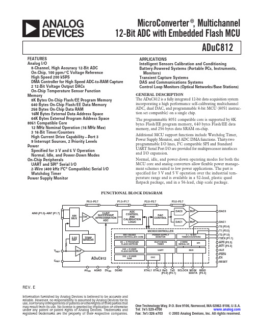
aADuC812Information furnished by Analog Devices is believed to be accurate andreliable. However, no responsibility is assumed by Analog Devices for its use, nor for any infringements of patents or other rights of third parties that may result from its use. No license is granted by implication or otherwise under any patent or patent rights of Analog Devices. Trademarks and registered trademarks are the property of their respective companies.One Technology Way, P.O. Box 9106, Norwood, MA 02062-9106, U.S.A.Tel: 781/329-4700 Fax: 781/326-8703© 2003 Analog Devices, Inc. All rights reserved.REV.EMicroConverter ®, Multichannel 12-Bit ADC with Embedded Flash MCUFUNCTIONAL BLOCK DIAGRAMSDATA (P3.3)(P3.1)(P3.0)DDDDT2 (P1.0)T2EX (P1.1) (P3.2) (P3.3)AIN0 (P1.0)–AIN7 (P1.7)V REFC REFFEATURES Analog I/O8-Channel, High Accuracy 12-Bit ADC On-Chip, 100 ppm/؇C Voltage Reference High Speed 200 kSPSDMA Controller for High Speed ADC-to-RAM Capture 2 12-Bit Voltage Output DACsOn-Chip Temperature Sensor Function Memory8K Bytes On-Chip Flash/EE Program Memory 640 Bytes On-Chip Flash/EE Data Memory 256 Bytes On-Chip Data RAM16M Bytes External Data Address Space 64K Bytes External Program Address Space 8051 Compatible Core12 MHz Nominal Operation (16 MHz Max)3 16-Bit Timer/CountersHigh Current Drive Capability—Port 39 Interrupt Sources, 2 Priority Levels PowerSpecified for 3 V and 5 V Operation Normal, Idle, and Power-Down Modes On-Chip PeripheralsUART and SPI ® Serial I/O2-Wire (400 kHz I 2C ® Compatible) Serial I/O Watchdog Timer Power Supply MonitorAPPLICATIONSIntelligent Sensors Calibration and ConditioningBattery-Powered Systems (Portable PCs, Instruments,Monitors)Transient Capture SystemsDAS and Communications SystemsControl Loop Monitors (Optical Networks/Base Stations)GENERAL DESCRIPTIONThe ADuC812 is a fully integrated 12-bit data acquisition system incorporating a high performance self-calibrating multichannel ADC, dual DAC, and programmable 8-bit MCU (8051 instruc-tion set compatible) on a single chip.The programmable 8051 compatible core is supported by 8K bytes Flash/EE program memory, 640 bytes Flash/EE data memory, and 256 bytes data SRAM on-chip.Additional MCU support functions include Watchdog Timer,Power Supply Monitor, and ADC DMA functions. Thirty-two programmable I/O lines, I 2C compatible SPI and Standard UART Serial Port I/O are provided for multiprocessor interfaces and I/O expansion.Normal, idle, and power-down operating modes for both the MCU core and analog converters allow flexible power manage-ment schemes suited to low power applications. The part is specified for 3 V and 5 V operation over the industrial tem-perature range and is available in a 52-lead, plastic quad flatpack package, and in a 56-lead, chip scale package.REV. EADuC812–2–FEATURES . . . . . . . . . . . . . . . . . . . . . . . . . . . . . . . . . . . . . . . .1APPLICATONS . . . . . . . . . . . . . . . . . . . . . . . . . . . . . . . . . . . . .1GENERAL DESCRIPTION . . . . . . . . . . . . . . . . . . . . . . . . . . .1SPECIFICATIONS . . . . . . . . . . . . . . . . . . . . . . . . . . . . . . . . . .3ABSOLUTE MAXIMUM RATINGS . . . . . . . . . . . . . . . . . . . .6PIN CONFIGURATIONS . . . . . . . . . . . . . . . . . . . . . . . . . . . . .6ORDERING GUIDE . . . . . . . . . . . . . . . . . . . . . . . . . . . . . . . . .6PIN FUNCTION DESCRIPTIONS . . . . . . . . . . . . . . . . . . . . .7TERMINOLOGY . . . . . . . . . . . . . . . . . . . . . . . . . . . . . . . . . . . .8ADC SPECIFICATIONS . . . . . . . . . . . . . . . . . . . . . . . . . . . . . .8Integral Nonlinearity . . . . . . . . . . . . . . . . . . . . . . . . . . . . . . . .8Differential Nonlinearity . . . . . . . . . . . . . . . . . . . . . . . . . . . . .8Offset Error . . . . . . . . . . . . . . . . . . . . . . . . . . . . . . . . . . . . . . .8Full-Scale Error . . . . . . . . . . . . . . . . . . . . . . . . . . . . . . . . . . . .8Signal to (Noise + Distortion) Ratio . . . . . . . . . . . . . . . . . . . .8Total Harmonic Distortion . . . . . . . . . . . . . . . . . . . . . . . . . . .8DAC SPECIFICATIONS . . . . . . . . . . . . . . . . . . . . . . . . . . . . . .8Relative Accuracy . . . . . . . . . . . . . . . . . . . . . . . . . . . . . . . . . . .8Voltage Output Settling Time . . . . . . . . . . . . . . . . . . . . . . . . .8Digital-to-Analog Glitch Impulse . . . . . . . . . . . . . . . . . . . . . . .8ARCHITECTURE, MAIN FEATURES . . . . . . . . . . . . . . . . . .9MEMORY ORGANIZATION . . . . . . . . . . . . . . . . . . . . . . . . . .9OVERVIEW OF MCU-RELATED SFRs . . . . . . . . . . . . . . . . .10Accumulator SFR . . . . . . . . . . . . . . . . . . . . . . . . . . . . . . . . .10B SFR . . . . . . . . . . . . . . . . . . . . . . . . . . . . . . . . . . . . . . . . . .10Stack Pointer SFR . . . . . . . . . . . . . . . . . . . . . . . . . . . . . . . . .10Data Pointer . . . . . . . . . . . . . . . . . . . . . . . . . . . . . . . . . . . . .10Program Status Word SFR . . . . . . . . . . . . . . . . . . . . . . . . . . .10Power Control SFR . . . . . . . . . . . . . . . . . . . . . . . . . . . . . . . .10SPECIAL FUNCTION REGISTERS . . . . . . . . . . . . . . . . . . .11ADC CIRCUIT INFORMATION . . . . . . . . . . . . . . . . . . . . . .12General Overview . . . . . . . . . . . . . . . . . . . . . . . . . . . . . . . . . .12ADC Transfer Function . . . . . . . . . . . . . . . . . . . . . . . . . . . . .12Typical Operation . . . . . . . . . . . . . . . . . . . . . . . . . . . . . . . . .12ADCCON1—(ADC Control SFR #1) . . . . . . . . . . . . . . . . .13ADCCON2—(ADC Control SFR #2) . . . . . . . . . . . . . . . . .14ADCCON3—(ADC Control SFR #3) . . . . . . . . . . . . . . . . .14Driving the ADC . . . . . . . . . . . . . . . . . . . . . . . . . . . . . . . . . .15Voltage Reference Connections . . . . . . . . . . . . . . . . . . . . . . .16Configuring the ADC . . . . . . . . . . . . . . . . . . . . . . . . . . . . . . .16 ADC DMA Mode . . . . . . . . . . . . . . . . . . . . . . . . . . . . . . . . .16DMA Mode Configuration Example . . . . . . . . . . . . . . . . . . .17 Micro Operation during ADC DMA Mode . . . . . . . . . . . . . .17Offset and Gain Calibration Coefficients . . . . . . . . . . . . . . . .17Calibration . . . . . . . . . . . . . . . . . . . . . . . . . . . . . . . . . . . . . . .18NONVOLATILE FLASH MEMORY . . . . . . . . . . . . . . . . . . .18Flash Memory Overview . . . . . . . . . . . . . . . . . . . . . . . . . . . .18Flash/EE Memory and the ADuC812 . . . . . . . . . . . . . . . . . .18ADuC812 Flash/EE Memory Reliability . . . . . . . . . . . . . . . .18Using the Flash/EE Program Memory . . . . . . . . . . . . . . . . . .19Using the Flash/EE Data Memory . . . . . . . . . . . . . . . . . . . . .19ECON—Flash/EE Memory Control SFR . . . . . . . . . . . . . . .20Flash/EE Memory Timing . . . . . . . . . . . . . . . . . . . . . . . . . . .20Using the Flash/EE Memory Interface . . . . . . . . . . . . . . . . . .20Erase-All . . . . . . . . . . . . . . . . . . . . . . . . . . . . . . . . . . . . . . . .20Program a Byte . . . . . . . . . . . . . . . . . . . . . . . . . . . . . . . . . . .20USER INTERFACE TO OTHER ON-CHIPADuC812 PERIPHERALS . . . . . . . . . . . . . . . . . . . . . . . . . . . .21Using the DAC . . . . . . . . . . . . . . . . . . . . . . . . . . . . . . . . . . .22WATCHDOG TIMER . . . . . . . . . . . . . . . . . . . . . . . . . . . . . . .24POWER SUPPLY MONITOR . . . . . . . . . . . . . . . . . . . . . . . . .24SERIAL PERIPHERAL INTERFACE . . . . . . . . . . . . . . . . . . .25MISO (Master In, Slave Out Data I/O Pin) . . . . . . . . . . . . . .25MOSI (Master Out, Slave In Pin) . . . . . . . . . . . . . . . . . . . . .26SCLOCK (Serial Clock I/O Pin) . . . . . . . . . . . . . . . . . . . . . .26SS (Slave Select Input Pin) . . . . . . . . . . . . . . . . . . . . . . . . . .26Using the SPI Interface . . . . . . . . . . . . . . . . . . . . . . . . . . . . .27SPI Interface—Master Mode . . . . . . . . . . . . . . . . . . . . . . . . .27SPI Interface—Slave Mode . . . . . . . . . . . . . . . . . . . . . . . . . .27I 2C COMPATIBLE INTERFACE . . . . . . . . . . . . . . . . . . . . . .288051 COMPATIBLE ON-CHIP PERIPHERALS . . . . . . . . . .29Parallel I/O Ports 0–3 . . . . . . . . . . . . . . . . . . . . . . . . . . . . . . .29Timers/Counters . . . . . . . . . . . . . . . . . . . . . . . . . . . . . . . . . .29Timer/Counters 0 and 1 Data Registers . . . . . . . . . . . . . . . . .31TH0 and TL0 . . . . . . . . . . . . . . . . . . . . . . . . . . . . . . . . . . . .31TH1 and TL1 . . . . . . . . . . . . . . . . . . . . . . . . . . . . . . . . . . . .31TIMER/COUNTERS 0 AND 1 OPERATING MODES . . . . .32Mode 0 (13-Bit Timer/Counter) . . . . . . . . . . . . . . . . . . . . . .32Mode 1 (16-Bit Timer/Counter) . . . . . . . . . . . . . . . . . . . . . .32Mode 2 (8-Bit Timer/Counter with Auto Reload) . . . . . . . . .32Mode 3 (Two 8-Bit Timer/Counters) . . . . . . . . . . . . . . . . . .32Timer/Counter 2 Data Registers . . . . . . . . . . . . . . . . . . . . . .33TH2 and TL2 . . . . . . . . . . . . . . . . . . . . . . . . . . . . . . . . . . . .33RCAP2H and RCAP2L . . . . . . . . . . . . . . . . . . . . . . . . . . . . .33Timer/Counter Operation Modes . . . . . . . . . . . . . . . . . . . . .3416-Bit Autoreload Mode . . . . . . . . . . . . . . . . . . . . . . . . . . . .3416-Bit Capture Mode . . . . . . . . . . . . . . . . . . . . . . . . . . . . . . .34UART SERIAL INTERFACE . . . . . . . . . . . . . . . . . . . . . . . . .35Mode 0 (8-Bit Shift Register Mode) . . . . . . . . . . . . . . . . . . .36Mode 1 (8-Bit UART, Variable Baud Rate) . . . . . . . . . . . . . .36Mode 2 (9-Bit UART with Fixed Baud Rate) . . . . . . . . . . . .36Mode 3 (9-Bit UART with Variable Baud Rate) . . . . . . . . . .36UART Serial Port Baud Rate Generation . . . . . . . . . . . . . . .36Timer 1 Generated Baud Rates . . . . . . . . . . . . . . . . . . . . . . .37Timer 2 Generated Baud Rates . . . . . . . . . . . . . . . . . . . . . . .37INTERRUPT SYSTEM . . . . . . . . . . . . . . . . . . . . . . . . . . . . . .38Interrupt Priority . . . . . . . . . . . . . . . . . . . . . . . . . . . . . . . . . .39Interrupt Vectors . . . . . . . . . . . . . . . . . . . . . . . . . . . . . . . . . .39ADuC812 HARDWARE DESIGN CONSIDERATIONS . . . .40Clock Oscillator . . . . . . . . . . . . . . . . . . . . . . . . . . . . . . . . . . .40External Memory Interface . . . . . . . . . . . . . . . . . . . . . . . . . .40Power-On Reset Operation . . . . . . . . . . . . . . . . . . . . . . . . . .41Power Supplies . . . . . . . . . . . . . . . . . . . . . . . . . . . . . . . . . . . .41Power Consumption . . . . . . . . . . . . . . . . . . . . . . . . . . . . . . .42Grounding and Board Layout Recommendations . . . . . . . . .43OTHER HARDWARE CONSIDERATIONS . . . . . . . . . . . . .44In-Circuit Serial Download Access . . . . . . . . . . . . . . . . . . . .44Embedded Serial Port Debugger . . . . . . . . . . . . . . . . . . . . . .44Single-Pin Emulation Mode . . . . . . . . . . . . . . . . . . . . . . . . . .45Enhanced-Hooks Emulation Mode . . . . . . . . . . . . . . . . . . . .45Typical System Configuration . . . . . . . . . . . . . . . . . . . . . . . .45QUICKSTART DEVELOPMENT SYSTEM . . . . . . . . . . . . .45Download—In-Circuit Serial Downloader . . . . . . . . . . . . . . .45DeBug—In-Circuit Debugger . . . . . . . . . . . . . . . . . . . . . . . .45ADSIM—Windows Simulator . . . . . . . . . . . . . . . . . . . . . . . .45TIMING SPECIFICATIONS . . . . . . . . . . . . . . . . . . . . . . . . .46OUTLINE DIMENSIONS . . . . . . . . . . . . . . . . . . . . . . . . . . . .56Revision History . . . . . . . . . . . . . . . . . . . . . . . . . . . . . . . . . . . .57TABLE OF CONTENTSADuC812 SPECIFICATIONS1, 2(AV DD = DV DD = 3.0 V or 5.0 V ؎ 10%, REF IN/REF OUT = 2.5 V Internal Reference, MCLKIN = 11.0592MHz, f SAMPLE = 200 kHz, DAC V OUT Load to AGND; R L = 2 k⍀, C L = 100 pF. All specifications T A = T MIN to T MAX, unless otherwise noted.)ADuC812BSParameter V DD = 5 V V DD = 3 V Unit Test Conditions/CommentsADC CHANNEL SPECIFICATIONSDC ACCURACY3, 4Resolution1212BitsIntegral Nonlinearity±1/2±1/2LSB typ f SAMPLE = 100 kHz±1.5±1.5LSB max f SAMPLE = 100 kHz±1.5±1.5LSB typ f SAMPLE = 200 kHz Differential Nonlinearity±1±1LSB typ f SAMPLE = 100 kHz. Guaranteed NoMissing Codes at 5 V CALIBRATED ENDPOINT ERRORS5, 6Offset Error±5±5LSB max±1±1LSB typOffset Error Match11LSB typGain Error±6±6LSB max±1±1LSB typGain Error Match 1.5 1.5LSB typUSER SYSTEM CALIBRATION7Offset Calibration Range±5±5% of V REF typGain Calibration Range±2.5±2.5% of V REF typDYNAMIC PERFORMANCE f IN = 10 kHz Sine Wavef SAMPLE = 100 kHzSignal-to-Noise Ratio (SNR)87070dB typTotal Harmonic Distortion (THD)–78–78dB typPeak Harmonic or Spurious Noise–78–78dB typANALOG INPUTInput Voltage Ranges0 to V REF0 to V REF VLeakage Current±1±1µA max±0.1±0.1µA typInput Capacitance92020pF maxTEMPERATURE SENSOR10Voltage Output at 25°C600600mV typ Can vary significantly (> ±20%) Voltage TC–3.0–3.0mV/°C typ from device to deviceDAC CHANNEL SPECIFICATIONSDC ACCURACY11Resolution1212BitsRelative Accuracy±3±3LSB typDifferential Nonlinearity±0.5±1LSB typ Guaranteed 12-Bit Monotonic Offset Error±60±60mV max±15±15mV typFull-Scale Error±30±30mV max±10±10mV typFull-Scale Mismatch±0.5±0.5% typ% of Full-Scale on DAC1 ANALOG OUTPUTSVoltage Range_00 to V REF0 to V REF V typVoltage Range_10 to V DD0 to V DD V typResistive Load1010kΩ typCapacitive Load100100pF typOutput Impedance0.50.5Ω typI SINK5050µA typREV. E–3–ADuC812SPECIFICATIONS1, 2 (continued)ADuC812BSParameter V DD = 5 V V DD = 3 V Unit Test Conditions/CommentsDAC AC CHARACTERISTICSVoltage Output Settling Time1515µs typ Full-Scale Settling Time towithin 1/2 LSB of Final Value Digital-to-Analog Glitch Energy1010nV sec typ 1 LSB Change at Major Carry REFERENCE INPUT/OUTPUTREF IN Input Voltage Range9 2.3/V DD 2.3/V DD V min/maxInput Impedance150150kΩ typREF OUT Output Voltage 2.5 ± 2.5% 2.5 ± 2.5%V min/max Initial Tolerance @ 25°C2.5 2.5V typREF OUT Tempco100100ppm/°C typFLASH/EE MEMORY PERFORMANCECHARACTERISTICS12, 13Endurance10,000Cycles min50,00050,000Cycles typData Retention10Years minWATCHDOG TIMERCHARACTERISTICSOscillator Frequency6464kHz typPOWER SUPPLY MONITORCHARACTERISTICSPower Supply Trip Point Accuracy±2.5±2.5% of SelectedNominal TripPoint Voltagemax±1.0±1.0% of SelectedNominal TripPoint VoltagetypDIGITAL INPUTSInput High Voltage (V INH) 2.4 2.4V minXTAL1 Input High Voltage (V INH) Only4V minInput Low Voltage (V INL)0.80.8V maxInput Leakage Current (Port0, EA)±10±10µA max V IN = 0 V or V DD±1±1µA typ V IN = 0 V or V DDLogic 1 Input Current(All Digital Inputs)±10±10µA max V IN = V DD±1±1µA typ V IN = V DDLogic 0 Input Current (Port 1, 2, 3)–80–40µA max–40–20µA typ V IL = 450 mVLogic 1-0 Transition Current (Port 1, 2, 3)–700–500µA max V IL = 2 V–400–200µA typ V IL = 2 VInput Capacitance1010pF typ–4–REV. EADuC812ADuC812BSParameter V DD = 5 V V DD = 3 V Unit Test Conditions/Comments DIGITAL OUTPUTSOutput High Voltage (V OH) 2.4 2.4V min V DD = 4.5 V to 5.5 VI SOURCE = 80 µA4.0 2.6V typ V DD = 2.7 V to 3.3 VI SOURCE = 20 µAOutput Low Voltage (V OL)ALE, PSEN, Ports 0 and 20.40.4V max I SINK = 1.6 mA0.20.2V typ I SINK = 1.6 mAPort 30.40.4V max I SINK = 8 mA0.20.2V typ I SINK = 8 mAFloating State Leakage Current±10±10µA max±1±1µA typFloating State Output Capacitance1010pF typPOWER REQUIREMENTS14, 15, 16I DD Normal Mode174325mA max MCLKIN = 16 MHz3216mA typ MCLKIN = 16 MHz2612mA typ MCLKIN = 12 MHz83mA typ MCLKIN = 1 MHzI DD Idle Mode2510mA max MCLKIN = 16 MHz186mA typ MCLKIN = 16 MHz156mA typ MCLKIN = 12 MHz72mA typ MCLKIN = 1 MHzI DD Power-Down Mode183015µA max55µA typNOTES1Specifications apply after calibration.2Temperature range –40°C to +85°C.3Linearity is guaranteed during normal MicroConverter core operation.4Linearity may degrade when programming or erasing the 640 byte Flash/EE space during ADC conversion times due to on-chip charge pump activity.5Measured in production at VDD = 5 V after Software Calibration Routine at 25°C only.6User may need to execute Software Calibration Routine to achieve these specifications, which are configuration dependent.7The offset and gain calibration spans are defined as the voltage range of user system offset and gain errors that the ADuC812 can compensate.8SNR calculation includes distortion and noise components.9Specification is not production tested, but is supported by characterization data at initial product release.10The temperature sensor will give a measure of the die temperature directly; air temperature can be inferred from this result.11DAC linearity is calculated using:Reduced code range of 48 to 4095, 0 to V REF rangeReduced code range of 48 to 3995, 0 to V DD rangeDAC output load = 10 kΩ and 50 pF.12Flash/EE Memory Performance Specifications are qualified as per JEDEC Specification (Data Retention) and JEDEC Draft Specification A117 (Endurance). 13Endurance Cycling is evaluated under the following conditions:Mode= Byte Programming, Page Erase CyclingCycle Pattern= 00H to FFHErase Time= 20 msProgram Time= 100 µs14IDDat other MCLKIN frequencies is typically given by:Normal Mode (V DD = 5 V):I DD = (1.6 nAs × MCLKIN) + 6 mANormal Mode (V DD = 3 V):I DD = (0.8 nAs × MCLKIN) + 3 mAIdle Mode (V DD = 5 V):I DD = (0.75 nAs × MCLKIN) + 6 mAIdle Mode (V DD = 3 V):I DD = (0.25 nAs × MCLKIN) + 3 mAwhere MCLKIN is the oscillator frequency in MHz and resultant I DD values are in mA.15IDD currents are expressed as a summation of analog and digital power supply currents during normal MicroConverter operation.16IDD is not measured during Flash/EE program or erase cycles; I DD will typically increase by 10 mA during these cycles.17Analog IDD = 2 mA (typ) in normal operation (internal V REF, ADC, and DAC peripherals powered on).18EA = Port0 = DVDD, XTAL1 (Input) tied to DV DD, during this measurement.Typical specifications are not production tested, but are supported by characterization data at initial product release.Timing Specifications—See Pages 46–55.Specifications subject to change without notice.Please refer to User Guide, Quick Reference Guide, Application Notes, and Silicon Errata Sheet at /microconverter for additional information.REV. E–5–REV. EADuC812–6–52-Lead MQFP0.7/A D 70.6/A D 60.5/A D 50.4/A D 4V D DG N D0.3/A D 30.2/A D 20.1/A D 10.0/A D 0L ES E N AP1.1/ADC1/T2EX P1.2/ADC2P1.3/ADC3AV DD AGND C REF V REF DAC0DAC1P1.4/ADC4P1.5/ADC5/SSP1.6/ADC6P2.7/A15/A23P2.6/A14/A22P2.5/A13/A21P2.4/A12/A20DGND DV DDXTAL2XTAL1P2.3/A11/A19P2.2/A10/A18P2.1/A9/A17P2.0/A8/A16SDATA/MOSIP 1.7/A D C 7R E S E TP 3.0/R x D P 3.1/T x DP 3.2/I N T 0P 3.3/I N T 1/M I S O D V D DD G N DP 3.4/T 0P 3.5/T 1/C O NV S TP 3.7/R DS C L O C KP 3.6/W RABSOLUTE MAXIMUM RATINGS *(T A = 25°C, unless otherwise noted.)AV DD to DV DD . . . . . . . . . . . . . . . . . . . . . . –0.3 V to +0.3 V AGND to DGND . . . . . . . . . . . . . . . . . . . . –0.3 V to +0.3 V DV DD to DGND, AV DD to AGND . . . . . . . . . –0.3 V to +7 V Digital Input Voltage to DGND . . . –0.3 V to DV DD + 0.3 V Digital Output Voltage to DGND . . –0.3 V to DV DD + 0.3 V V REF to AGND . . . . . . . . . . . . . . . . . –0.3 V to AV DD + 0.3 V Analog Inputs to AGND . . . . . . . . . . –0.3 V to AV DD + 0.3 V Operating Temperature Range Industrial (B Version). . . . . . . . . . . . . . . . . . . . . . . . . . . . . . . . . . –40°C to +85°CCAUTIONE SD (electrostatic discharge) sensitive device. E lectrostatic charges as high as 4000V readily accumulate on the human body and test equipment and can discharge without detection. Although the ADuC812 features proprietary ESD protection circuitry, permanent damage may occur on devices subjected to high energy electrostatic discharges. Therefore, proper ESD precautions are recommended to avoid performance degradation or loss of functionality.56-Lead LFCSPP1.1/ADC1/T2EXP1.2/ADC2P1.3/ADC3AV DD AV DD C V P1.4/ADC4P1.5/ADC5/SSP 1.6/A D C P 1.7/A D C R E S E P 3.0/R X P 3.1/T X DD /MOSIS C L O C P 3.7/R P 3.6/W P 3.5/T 1/C O N V S P 3.4/T D G N D V D P 3.3/I N T 1/M I S P 3.2/I N T 1.0/A D C 0/T 20.7/A D 70.6/A D 60.5/A D 50.4/A D 4V D DG N D0.3/A D 30.2/A D 20.1/A D 10.0/A D 0L ES E N AORDERING GUIDETemperature Package Package ModelRange DescriptionOption ADuC812BS –40°C to +85°C 52-Lead Metric Quad Flat PackageS-52ADuC812BS –40°C to +85°C 56-Lead Lead Frame Chip Scale Package CP-56EVAL-ADuC812QS QuickStart Development SystemEVAL-ADuC812QSPQuickStart Development System PlusPIN CONFIGURATIONSStorage Temperature Range . . . . . . . . . . . . –65°C to +150°C Junction Temperature . . . . . . . . . . . . . . . . . . . . . . . . . 150°C θJA Thermal Impedance . . . . . . . . . . . . . . . . . . . . . . . 90°C/W Lead Temperature, SolderingVapor Phase (60 sec) . . . . . . . . . . . . . . . . . . . . . . . . 215°C Infrared (15 sec) . . . . . . . . . . . . . . . . . . . . . . . . . . . 220°C*Stresses above those listed under Absolute Maximum Ratings may cause perma-nent damage to the device. This is a stress rating only; functional operation of the device at these or any other conditions above those listed in the operational sections of this specification is not implied. Exposure to absolute maximum rating conditions for extended periods may affect device reliability.REV. E ADuC812–7–PIN FUNCTION DESCRIPTIONSMnemonic Type Function DV DD P Digital Positive Supply Voltage, 3 V or 5 V Nominal.AV DD P Analog Positive Supply Voltage, 3 V or 5 V Nominal.C REF I Decoupling Input for On-Chip Reference. Connect 0.1 µF between this pin and AGND.V REFI/OReference Input/Output. This pin is connected to the internal reference through a series resistor and is the reference source for the ADC. The nominal internal reference voltage is 2.5 V, which appears at the pin.This pin can be overdriven by an external reference.AGND G Analog Ground. Ground reference point for the analog circuitry.P1.0–P1.7IPort 1 is an 8-bit input port only. Unlike other ports, Port 1 defaults to Analog Input mode. To configure any of these Port Pins as a digital input, write a 0 to the port bit. Port 1 pins are multifunctional and share the following functionality.ADC0–ADC7I Analog Inputs. Eight single-ended analog inputs. Channel selection is via ADCCON2 SFR.T2I Timer 2 Digital Input. Input to Timer/Counter 2. When enabled, Counter 2 is incremented in response to a 1 to 0 transition of the T2 input.T2EX I Digital Input. Capture/Reload trigger for Counter 2; also functions as an Up/Down control input for Counter 2.SSI Slave Select Input for the SPI Interface.SDATA I/O User selectable, I 2C Compatible or SPI Data Input/Output Pin.SCLOCK I/O Serial Clock Pin for I 2C Compatible or SPI Serial Interface Clock.MOSI I/O SPI Master Output/Slave Input Data I/O Pin for SPI Interface.MISO I/O SPI Master Input/Slave Output Data I/O Pin for SPI Serial Interface.DAC0O Voltage Output from DAC0.DAC1O Voltage Output from DAC1.RESETIDigital Input. A high level on this pin for 24 master clock cycles while the oscillator is running resets the device. External power-on reset (POR) circuity must be implemented to drive the RESET pin as described in the Power-On Reset Operation section.P3.0–P3.7I/OPort 3 is a bidirectional port with internal pull-up resistors. Port 3 pins that have 1s written to them are pulled high by the internal pull-up resistors; in that state they can be used as inputs. As inputs, Port 3 pins being pulled externally low will source current because of the internal pull-up resistors. Port 3 pins also contain various secondary functions that are described below.RxD I/O Receiver Data Input (Asynchronous) or Data Input/Output (Synchronous) of Serial (UART) Port TxD O Transmitter Data Output (Asynchronous) or Clock Output (Synchronous) of Serial (UART) PortINT0I Interrupt 0, programmable edge or level triggered Interrupt input, INT0 can be programmed to one of two priority levels. This pin can also be used as a gate control input to Timer 0.INT1I Interrupt 1, programmable edge or level triggered Interrupt input, INT1 can be programmed to one of two priority levels. This pin can also be used as a gate control input to Timer 1.T0I Timer/Counter 0 Input.T1I Timer/Counter 1 Input.CONVST I Active Low Convert Start Logic Input for the ADC Block when the External Convert Start Function is Enabled.A low-to-high transition on this input puts the track-and-hold into its hold mode and starts conversion.WR O Write Control Signal, Logic Output. Latches the data byte from Port 0 into the external data memory.RD O Read Control Signal, Logic Output. Enables the external data memory to Port 0.XTAL2O Output of the Inverting Oscillator Amplifier.XTAL1I Input to the Inverting Oscillator Amplifier and to the Internal Clock Generator Circuits.DGND G Digital Ground. Ground reference point for the digital circuitry.P2.0–P2.7I/OPort 2 is a bidirectional port with internal pull-up resistors. Port 2 pins that have 1s written to them are (A8–A15)pulled high by the internal pull-up resistors; in that state they can be used as inputs. As inputs, Port 2(A16–A23)pins being pulled externally low will source current because of the internal pull-up resistors. Port 2 emits the high order address bytes during fetches from external program memory and middle and high order address bytes during accesses to the external 24-bit external data memory space.REV. EADuC812–8–Mnemonic Type Function PSENOProgram Store Enable, Logic Output. This output is a control signal that enables the external program memory to the bus during external fetch operations. It is active every six oscillator periods except during external data memory accesses. This pin remains high during internal program execution. PSEN can also be used to enable serial download mode when pulled low through a resistor on power-up or RESET.ALE OAddress Latch Enable, Logic Output. This output is used to latch the low byte (and page byte for 24-bit address space accesses) of the address into external memory during normal operation. It is activated every six oscillator periods except during an external data memory access.EA IExternal Access Enable, Logic Input. When held high, this input enables the device to fetch code frominternal program memory locations 0000H to 1FFFH. When held low, this input enables the device to fetch all instructions from external program memory.P0.7–P0.0I/OPort 0 is an 8-bit open-drain bidirectional I/O port. Port 0 pins that have 1s written to them float and in (A0–A7)that state can be used as high impedance inputs. Port 0 is also the multiplexed low order address and data bus during accesses to external program or data memory. In this application, it uses strong internal pull-ups when emitting 1s.TERMINOLOGYADC SPECIFICATIONS Integral NonlinearityThis is the maximum deviation of any code from a straight line passing through the endpoints of the ADC transfer function.The endpoints of the transfer function are zero scale, a point 1/2 LSB below the first code transition, and full scale, a point 1/2 LSB above the last code transition.Differential NonlinearityThis is the difference between the measured and the ideal 1LSB change between any two adjacent codes in the ADC.Offset ErrorThis is the deviation of the first code transition (0000...000)to (0000...001) from the ideal, i.e., +1/2 LSB.Full-Scale ErrorThis is the deviation of the last code transition from the ideal AIN voltage (Full Scale – 1.5 LSB) after the offset error has been adjusted out.Signal-to-(Noise + Distortion) RatioThis is the measured ratio of signal-to-(noise + distortion) at the output of the ADC. The signal is the rms amplitude of the fun-damental. Noise is the rms sum of all nonfundamental signals up to half the sampling frequency (f S /2), excluding dc. The ratio isdependent upon the number of quantization levels in the digiti-zation process; the more levels, the smaller the quantization noise. The theoretical signal-to-(noise + distortion) ratio for an ideal N-bit converter with a sine wave input is given by:Signal-to-(Noise + Distortion ) = (6.02N + 1.76) dBThus for a 12-bit converter, this is 74 dB.Total Harmonic DistortionTotal Harmonic Distortion is the ratio of the rms sum of the harmonics to the fundamental.DAC SPECIFICATIONS Relative AccuracyRelative accuracy or endpoint linearity is a measure of the maximum deviation from a straight line passing through the endpoints of the DAC transfer function. It is measured after adjusting for zero-scale error and full-scale error.Voltage Output Settling TimeThis is the amount of time it takes for the output to settle to a specified level for a full-scale input change.Digital-to-Analog Glitch ImpulseThis is the amount of charge injected into the analog output when the inputs change state. It is specified as the area of the glitch in nV sec.PIN FUNCTION DESCRIPTIONS (continued)。
- 1、下载文档前请自行甄别文档内容的完整性,平台不提供额外的编辑、内容补充、找答案等附加服务。
- 2、"仅部分预览"的文档,不可在线预览部分如存在完整性等问题,可反馈申请退款(可完整预览的文档不适用该条件!)。
- 3、如文档侵犯您的权益,请联系客服反馈,我们会尽快为您处理(人工客服工作时间:9:00-18:30)。
浅谈ADμC812数字平台在中职单片机教学中的应用
一、ADμC812MicroConverter介绍1硬件方面
ADμC812是全集成的12位数据采集系统,它包含了高性能的自校准8通道、高精度12位的ADC、高速ADC至RAM捕获(capture)DMA控制器、两个12位电压输出DAC以及8位MCU:额定工作频率12MHz(最大16MHz),3个16位定时器/计数器,32条可编程的I/O线,高电流驱动能力――端口3,9个中断源,2个优先级。
ADμC812片内有8K字节的闪速/电擦除(Flash/EE)程序存储器(支持PC在线编程不需要烧写器)、640字节的闪速/电擦除数据存储器以及256字节数据SRAM支持可编程、与8051兼容。
片外有16M的外部数据地址空间和64K字节的外部程序地址空间。
另外MCU支持的功能包括看门狗定时器、电源监视器以及ADC DMA功能。
位多处理器接口和I/O扩展提供了32条可编程的I/O线、IC兼容的SPI和标准的URAT串行端口I/O。
MCU内核和模拟转换器均有正常、空闲以及掉电工作模式,可提供适合于低功率应用的电源管理方案。
器件包括在工业温度范围内用3V或5V电压工作的两种规格。
ADμC812是从8051基础上发展起来的,与8051几乎完全兼容,为学生学习研究提供了范本。
2软件方面
生产商提供了ADμC812的开发系统QuitStart。
QuitStart 是功能完善、价格低廉的ADμC812的开发工具包,包括下列基于PC(Win95、98、Me、Xp兼容)的硬件和软件开发工具:代码开发、代码下载、代码调试。
二、ADμC812数字平台在中职单片机教学中的应用1利用ADμC812仿真器让单片机教学由抽象到具体
单片机课程之所以难,是因为其太抽象:①所有组成和工作过程都在芯片里面;②程序逻辑性强,其执行过程也在芯片内部。
而ADμC812仿真器由芯片开发商提供图形化仿真调试工具,从而使单片机内部结构一目了然。
尤其是ADμC812仿真器完全摆脱了以往调试工具的局限性,而且可以不需要硬件支持且功能完善,只要有电脑就可以让学生有更多的时间和机会来学习研究单片机。
由于所有的调试和仿真都是在电脑上进行的,几乎没什么成本,也不会造成什么损失。
而器件损坏是传统单片机实验实训经常发生的。
2利用ADμC812仿真器切实开展项目教学和课题研究
QuitStart是由生产商提供的ADμC812的开发工具包,其仿真的结果就是真实单片机运行的结果,从而使得大量的程序开发和调试过程完全软化。
这样不但使学生在学习过程中可以验证所学的知识,加深对所学知识的理解,而且让学生在一节课的时间内完成程序设计和调试成为可能。
再者这种开发只要有电脑几
乎也不受时空限制,可以让学生在有限硬件资源的情况下进行较大课题的研究,从而大大提高学生的动手和实践、科研能力。
3充分利用ADμC812的性能和特点,让学生在解决实际问题过程中提升能力
ADμC812仿真器并非纯软件模拟,而是QuitStart开发系统一部分只要通过ADμC812仿真器模拟分析认为正确程序就可以下载到ADμC812芯片中运行。
ADμC812采用支持在线可重新编程的代码和数据存储空间,而ADμC812仍位于应用硬件中。
另外ADμC812的兼容性好,自身集成了ADC、DAC,使系统的建立更加方便。
这样学生可边做边学、边做边改,使程序很容易得到验证,甚至可以直接用于实际电路中,让学生在在成功中激励自我提高。
综上所述,将ADμC812数字平台引入中职单片机教学中不仅可以改变目前中职单片机教学的现状,更重要的是:ADμC812成本很低,学生可以承受。
这样学生即使不在单片机实验室里,甚至不再学习单片机这门课了,只要学会了ADμC812数字平台,那他们照样可以进行单片机的学习、开发、研究、应用。
我想,这才是我国数字化技术人才的培养之道!。