STB5105-MBoard schematic
清华紫光 文诚系列电脑 说明书

文诚系列技术培训手册清华紫光台式电脑事业部技术支持部2004-06-01目录一、产品特点1.1优良的品质保证1.2出色的结构设计1.3可靠的安全维护二、文诚系列主机配置2.1文诚系列主机配置表三、主板技术规格3.1 精英P6VEMD2主板说明3.2 精英L4S5MG/GX+主板说明3.3 技嘉GA-8I845GV-CH2说明四、驱动程序安装4.1驱动光盘说明4.2驱动程序安装目录一、产品特点文诚系列电脑强调性能价格比,适用于教育、网吧等中低端用户,便于集中管理,统一维护。
1.1优良的品质保证1)通过国家3C认证;2)严格的部件优选体制,所有部件采用业界一线厂商的产品;3)周密的测试全集,保证部件的兼容性,同时保证系统的稳定性;4)五年保修。
1.2出色的结构设计1)立卧两用,根据不同空间随意放置;2)机箱面板模块化设计,根据不同的应用选取不同外观;3)良好的散热设计,确保立卧使用时系统内部热量有效、及时的散发;4)静音设计,减少部件共振,优化风道,降低噪音。
1.3可靠的安全维护1)集成硬盘保护功能,保证硬盘数据的安全,遭到破坏一键恢复;2)同一机型间网络传输功能,维护好一台机器即可通过网络对其他机器进行维护;3)自动维护,无人值班的情况下对整个网络环境中的机器机型维护;4)预留机箱锁孔,防止非法开启机箱。
二、文诚系列主机配置(一)文诚500 文诚800 文诚1000E 文诚1100文诚1200 CPU C3800Celeron 1.8GCeleron 1.8G Celeron 1.8G Celeron 1.8G主板 P6VEMD2L4S5MG/GX+ L4S5MG/GX+ L4S5MG/GX+GA-8I845GV-CH2内存Twinmos 128MDDR333Twinmos 128MDDR333Twinmos 128MDDR333Twinmos 128MDDR333Twinmos 128MDDR333硬盘SeagateST340015ASamsungSV0411N(40GB/5400PRM)SeagateST340015ASamsungSV0411N(40GB/5400PRM)SeagateST340015ASamsungSV0411N(40GB/5400PRM)光驱LG CR-8523B LG GCR-8523B软驱SamsungSFD-321BSamsungSFD-321BSamsungSFD-321B显示卡主板集成主板集成主板集成主板集成主板集成声卡主板集成主板集成主板集成主板集成主板集成网卡主板集成主板集成主板集成主板集成主板集成电源长城 1801-HP 长城 1801-HP 长城 1801-HP 长城 1801-HP 长城 1801-HPCPU风扇主板集成Cool MasterDI4-7H53B/DI4-7H54A-R2Cool MasterDI4-7H53B/DI4-7H54A-R2Cool MasterDI4-7H53B/DI4-7H54A-R2/EC203MBCool MasterDI4-7H53B/DI4-7H54A-R2/EC203MB机箱保利得 EN7472 保利得 EN7472 保利得 EN7472 保利得 EN7472 保利得 EN7472键盘精模 JME7010 精模 JME7010 精模 JME7010 精模 JME7010 精模 JME7010鼠标致伸 M042K0 致伸 M042K0 致伸 M042K0 致伸 M042K0 致伸 M042K0驱动光盘智能驱动光盘V2.0智能驱动光盘V2.0智能驱动光盘V2.0/2.1智能驱动光盘V2.0文诚系列主机配置(二)三、主板技术规格3.1文诚500采用的主板是:精英P6VEMD2,采用VIA CLE266 CE / VT8235 CD 芯片组。
LM5105中文资料
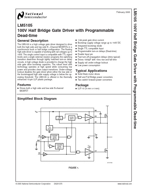
LM5105100V Half Bridge Gate Driver with Programmable Dead-timeGeneral DescriptionThe LM5105is a high voltage gate driver designed to drive both the high side and low side N –Channel MOSFETs in a synchronous buck or half bridge configuration.The floating high-side driver is capable of working with rail voltages up to 100V.The single control input is compatible with TTL signal levels and a single external resistor programs the switching transition dead-time through tightly matched turn-on delay circuits.A high voltage diode is provided to charge the high side gate drive bootstrap capacitor.The robust level shift technology operates at high speed while consuming low power and provides clean output transitions.Under-voltage lockout disables the gate driver when either the low side or the bootstrapped high side supply voltage is below the op-erating threshold.The LM5105is offered in the thermally enhanced 10-pin LLP plastic package.Featuresn Drives both a high side and low side N-channel MOSFETn 1.8A peak gate drive currentn Bootstrap supply voltage range up to 118V DC n Integrated bootstrap diode n Single TTL compatible Inputn Programmable turn-on delays (Dead-time)n Enable Input pinn Fast turn-off propagation delays (26ns typical)n Drives 1000pF with 15ns rise and fall time n Supply rail under-voltage lockout nLow power consumptionTypical Applicationsn Solid State motor drivesn Half and Full Bridge power converters n Two switch forward power convertersPackagen LLP-10(4mm x 4mm)Simplified Block Diagram20137502FIGURE 1.February 2005LM5105100V Half Bridge Gate Driver with Programmable Dead-time©2005National Semiconductor Corporation Connection Diagram2013750110-Lead LLPSee NS Number SDC10AOrdering InformationOrdering Number Package TypeNSC Package DrawingSupplied AsLM5105SD LLP-10SDC10A 1000shipped as Tape &Reel LM5105SDXLLP-10SDC10A4500shipped as Tape &ReelPin DescriptionsPin Name DescriptionApplication Information1V DD Positive gate drive supply Decouple VDD to VSS using a low ESR/ESL capacitor,placed as close to the IC as possible.2HBHigh side gate driver bootstrap rail Connect the positive terminal of bootstrap capacitor to the HB pin and connect negative terminal to HS.The Bootstrap capacitor should be placed as close to IC as possible.3HO High side gate driver outputConnect to the gate of high side N-MOS device through a short,low inductance path.4HS High side MOSFET source connection Connect to the negative terminal of the bootststrap capacitor and to the source of the high side N-MOS device.5NC Not Connected6RDTDeadtime programming pinA resistor from RDT to VSS programs the turn-on delay of both the high and low side MOSFETs.The resistor should be placed close to the IC to minimize noise coupling from adjacent PC board traces.7EN Logic input for driver Disable/EnableTTL compatible threshold with hysteresis.LO and HO are held in the low state when EN is low.8IN Logic input for gate driver TTL compatible threshold with hysteresis.The high side MOSFET is turned on and the low side MOSFET turned off when IN is high.9V SS Ground returnAll signals are referenced to this ground.10LOLow side gate driver outputConnect to the gate of the low side N-MOS device with a short,low inductance path.L M 5105 2Absolute Maximum Ratings(Note1)If Military/Aerospace specified devices are required, please contact the National Semiconductor Sales Office/ Distributors for availability and specifications.V DD to V SS–0.3V to+18VHB to HS–0.3V to+18VIN and EN to V SS–0.3V to V DD+0.3VLO to V SS–0.3V to V DD+0.3VHO to V SS HS–0.3V to HB+0.3VHS to V SS(Note6)−5V to+100VHB to V SS118VRDT to V SS–0.3V to5VJunction Temperature+150˚CStorage Temperature Range–55˚C to+150˚C ESD Rating HBM(Note2)2kVRecommended Operating ConditionsV DD+8V to+14V HS(Note6)–1V to100V HB HS+8V to HS+14V HS Slew Rate<50V/ns Junction Temperature–40˚C to+125˚CElectrical Characteristics Specifications in standard typeface are for TJ=+25˚C,and those in boldfacetype apply over the full operating junction temperature range.Unless otherwise specified,V DD=HB=12V,V SS=HS=0V,EN=5V.No load on LO or HO.RDT=100kΩ(Note4).Symbol Parameter Conditions Min Typ Max Units SUPPLY CURRENTSI DD V DD Quiescent Current IN=EN=0V0.340.6mAI DDO V DD Operating Current f=500kHz 1.653mAI HB Total HB Quiescent Current IN=EN=0V0.060.2mAI HBO Total HB Operating Current f=500kHz 1.33mAI HBS HB to V SS Current,Quiescent HS=HB=100V0.0510µAI HBSO HB to V SS Current,Operating f=500kHz0.1mAINPUT IN and ENV IL Low Level Input Voltage Threshold0.8 1.8VV IH High Level Input Voltage Threshold 1.8 2.2VR pd Input Pulldown Resistance Pin IN and EN100200500kΩDEAD-TIME CONTROLSVRDT Nominal Voltage at RDT 2.73 3.3VIRDT RDT Pin Current Limit RDT=0V0.75 1.5 2.25mA UNDER VOLTAGE PROTECTIONV DDR V DD Rising Threshold 6.0 6.97.4VV DDH V DD Threshold Hysteresis0.5VV HBR HB Rising Threshold 5.7 6.67.1VV HBH HB Threshold Hysteresis0.4VBOOT STRAP DIODEV DL Low-Current Forward Voltage I VDD-HB=100µA0.60.9VV DH High-Current Forward Voltage I VDD-HB=100mA0.85 1.1VR D Dynamic Resistance I VDD-HB=100mA0.8 1.5ΩLO GATE DRIVERV OLL Low-Level Output Voltage I LO=100mA0.250.4VV OHL High-Level Output Voltage I LO=–100mA,V OHL=V DD–V LO0.350.55VI OHL Peak Pullup Current LO=0V 1.8AI OLL Peak Pulldown Current LO=12V 1.6AHO GATE DRIVERV OLH Low-Level Output Voltage I HO=100mA0.250.4VV OHH High-Level Output Voltage I HO=–100mA,V OHH=HB–HO0.350.55VI OHH Peak Pullup Current HO=0V 1.8ALM51053Electrical Characteristics Specifications in standard typeface are for T J =+25˚C,and those in boldface typeapply over the full operating junction temperature range .Unless otherwise specified,V DD =HB =12V,V SS =HS =0V,EN =5V.No load on LO or HO.RDT=100k Ω(Note 4).(Continued)Symbol ParameterConditionsMinTyp MaxUnits I OLH Peak Pulldown CurrentHO =12V1.6ATHERMAL RESISTANCEθJAJunction to Ambient(Note 3),(Note 5)40˚C/WSwitching CharacteristicsSpecifications in standard typeface are for T J =+25˚C,and those in boldfacetype apply over the full operating junction temperature range .Unless otherwise specified,V DD =HB =12V,V SS =HS =0V,No Load on LO or HO (Note 4).Symbol ParameterConditionsMinTyp Max Units t LPHL Lower Turn-Off Propagation Delay 2656ns t HPHL Upper Turn-Off Propagation Delay 2656ns t LPLH Lower Turn-On Propagation Delay RDT =100k 485595705ns t HPLH Upper Turn-On Propagation Delay RDT =100k 485595705ns t LPLH Lower Turn-On Propagation Delay RDT =10k 75105150ns t HPLH Upper Turn-On Propagation Delay RDT =10k75105150ns t en ,t sd Enable and Shutdown propagation delay 28ns DT1,DT2Dead-time LO OFF to HO ON &HO OFF to LO ONRDT =100k 570µsRDT =10k 80MDT Dead-time matching RDT =100k 50t R ,t F Either Output Rise/Fall TimeC L =1000pF15t BSBootstrap Diode Turn-On or Turn-Off TimeI F =20mA,I R =200mA 50nsNote 1:Absolute Maximum Ratings indicate limits beyond which damage to the component may occur.Operating Ratings are conditions under which operation of the device is guaranteed.Operating Ratings do not imply guaranteed performance limits.For guaranteed performance limits and associated test conditions,see the Electrical Characteristics tables.Note 2:The human body model is a 100pF capacitor discharged through a 1.5k Ωresistor into each pin.Pin 2,Pin 3and Pin 4are rated at 500V.Note 3:4layer board with Cu finished thickness 1.5/1.0/1.0/1.5oz.Maximum die size used.5x body length of Cu trace on PCB top.50x 50mm ground and power planes embedded in PCB.See Application Note AN-1187.Note 4:Min and Max limits are 100%production tested at 25˚C.Limits over the operating temperature range are guaranteed through correlation using Statistical Quality Control (SQC)methods.Limits are used to calculate National’s Average Outgoing Quality Level (AOQL).Note 5:The θJA is not a constant for the package and depends on the printed circuit board design and the operating conditions.Note 6:In the application the HS node is clamped by the body diode of the external lower N-MOSFET,therefore the HS voltage will generally not exceed -1V.However in some applications,board resistance and inductance may result in the HS node exceeding this stated voltage transiently.If negative transients occur on HS,the HS voltage must never be more negative than V DD -15V.For example,if V DD =10V,the negative transients at HS must not exceed -5V.L M 5105 4Typical Performance CharacteristicsV DD Operating Current vs Frequency Operating Current vs Temperature2013751020137511 Quiescent Current vs Supply Voltage Quiescent Current vs Temperature2013751220137513 HB Operating Current vs Frequency HO&LO Peak Output Current vs Output Voltage2013751620137517LM51055Typical Performance Characteristics(Continued)Diode Forward VoltageUndervoltage Hysteresis vs Temperature2013751520137518Undervoltage Rising Threshold vs Temperature LO &HO -High Level Output Voltage vs Temperature2013751920137520LO &HO -Low Level Output Voltage vs Temperature Input Threshold vs Temperature2013752120137522L M 5105 6Typical Performance Characteristics(Continued)Dead-Time vs RT Resistor ValueDead-Time vs Temperature (RT =10k)2013751420137526Dead-Time vs Temperature (RT =100k)20137527LM51057Timing DiagramsOperational NotesThe LM5105is a single PWM input Gate Driver with Enable that offers a programmable deadtime.The deadtime is set with a resistor at the RDT pin and can be adjusted from 100ns to 600ns.The wide deadtime programming range provides the flexibility to optimize drive signal timing for a wide range of MOSFETS and applications.The RDT pin is biased at 3V and current limited to 1mA maximum programming current.The time delay generator will accommodate resistor values from 5k to 100k with a deadtime time that is proportional to the RDT resistance.Grounding the RDT pin programs the LM5105to drive both outputs with minimum deadtime.STARTUP AND UVLOBoth top and bottom drivers include under-voltage lockout (UVLO)protection circuitry which monitors the supply volt-age (V DD )and bootstrap capacitor voltage (HB –HS)inde-pendently.The UVLO circuit inhibits each driver until suffi-cient supply voltage is available to turn-on the external MOSFETs,and the UVLO hysteresis prevents chattering during supply voltage transitions.When the supply voltage is applied to the V DD pin of LM5105,the top and bottom gates are held low until V DD exceeds the UVLO threshold,typically about 6.9V.Any UVLO condition on the bootstrap capacitor will disable only the high side output (HO).20137503LM5105Input -Output WaveformsFIGURE 2.20137504LM5105Switching Time Definitions:t LPLH ,t LPHL ,t HPLH ,t HPHLFIGURE 3.20137530LM5105Enable:t sdFIGURE 4.20137531LM5105Dead-time:DTFIGURE 5.L M 5105 8Operational Notes(Continued)LAYOUT CONSIDERATIONSThe optimum performance of high and low side gate drivers cannot be achieved without taking due considerations during circuit board layout.Following points are emphasized.1.A low ESR/ESL capacitor must be connected close tothe IC,and between V DD and V SS pins and between HB and HS pins to support high peak currents being drawn from V DD during turn-on of the external MOSFET.2.To prevent large voltage transients at the drain of the topMOSFET,a low ESR electrolytic capacitor must be con-nected between MOSFET drain and ground(V SS).3.In order to avoid large negative transients on the switchnode(HS)pin,the parasitic inductances in the source of top MOSFET and in the drain of the bottom MOSFET (synchronous rectifier)must be minimized.4.Grounding considerations:a)The first priority in designing grounding connections isto confine the high peak currents from charging and discharging the MOSFET gate in a minimal physical area.This will decrease the loop inductance and mini-mize noise issues on the gate terminal of the MOSFET.The MOSFETs should be placed as close as possible to the gate driver.b)The second high current path includes the bootstrapcapacitor,the bootstrap diode,the local ground refer-enced bypass capacitor and low side MOSFET body diode.The bootstrap capacitor is recharged on the cycle-by-cycle basis through the bootstrap diode from the ground referenced V DD bypass capacitor.The re-charging occurs in a short time interval and involves high peak current.Minimizing this loop length and area on the circuit board is important to ensure reliable operation.5.The resistor on the RDT pin must be placed very close tothe IC and seperated from high current paths to avoid noise coupling to the time delay generator which could disrupt timer operation.POWER DISSIPATION CONSIDERATIONSThe total IC power dissipation is the sum of the gate driverlosses and the bootstrap diode losses.The gate driverlosses are related to the switching frequency(f),output loadcapacitance on LO and HO(C L),and supply voltage(V DD)and can be roughly calculated as:P DGATES=2•f•C L•V DD2There are some additional losses in the gate drivers due tothe internal CMOS stages used to buffer the LO and HOoutputs.The following plot shows the measured gate driverpower dissipation versus frequency and load capacitance.Athigher frequencies and load capacitance values,the powerdissipation is dominated by the power losses driving theoutput loads and agrees well with the above equation.Thisplot can be used to approximate the power losses due to thegate drivers.Gate Driver Power Dissipation(LO+HO)V CC=12V,Neglecting Diode Losses20137505 The bootstrap diode power loss is the sum of the forwardbias power loss that occurs while charging the bootstrapcapacitor and the reverse bias power loss that occurs duringreverse recovery.Since each of these events happens onceper cycle,the diode power loss is proportional to frequency.Larger capacitive loads require more current to recharge thebootstrap capacitor resulting in more losses.Higher inputvoltages(V IN)to the half bridge result in higher reverserecovery losses.The following plot was generated based oncalculations and lab measurements of the diode recoverytime and current under several operating conditions.Thiscan be useful for approximating the diode power dissipation.LM51059Operational Notes(Continued)Diode Power Dissipation V IN =80V20137506Diode Power Dissipation V IN =40V20137507The total IC power dissipation can be estimated from the above plots by summing the gate drive losses with the bootstrap diode losses for the intended application.Because the diode losses can be significant,an external diode placed in parallel with the internal bootstrap diode (refer to Figure 6)and can be helpful in removing power from the IC.For this to be effective,the external diode must be placed close to the IC to minimize series inductance and have a significantly lower forward voltage drop than the internal diode.HS Transient Voltages Below GroundThe HS node will always be clamped by the body diode of the lower external FET.In some situations,board resis-tances and inductances can cause the HS node to tran-siently swing several volts below ground.The HS node can swing below ground provided:1.HS must always be at a lower potential than HO.Pulling HO more than -0.3V below HS can activate parasitic transistors resulting in excessive current to flow from the HB supply possibly resulting in damage to the IC.The same relationship is true with LO and VSS.If necessary,a Schottky diode can be placed externally between HO and HS or LO and GND to protect the IC from this type of transient.The diode must be placed as close to the IC pins as possible in order to be effective.2.HB to HS operating voltage should be 15V or less .Hence,if the HS pin transient voltage is -5V,VDD should be ideally limited to 10V to keep HB to HS below 15V.3.A low ESR bypass capacitor between HB to HS as wellas VCC to VSS is essential for proper operation.The capacitor should be located at the leads of the IC to minimize series inductance.The peak currents from LO and HO can be quite large.Any series inductances with the bypass capacitor will cause voltage ringing at the leads of the IC which must be avoided for reliable op-eration.L M 5105 10LM5105 Operational Notes(Continued)LM5105Driving MOSFETs Connected in Half-Bridge Configuration Array20137508FIGURE6.11Physical Dimensionsinches (millimeters)unless otherwise notedNotes:Unless otherwise specified1.Standard lead finish to be 200microinches/5.00micrometers minimum tin/lead (solder)on copper.2.Pin 1identification to have half of full circle option.3.No JEDEC registration as of Feb.2000.LLP-10Outline Drawing NS Package Number SDC10ANational does not assume any responsibility for use of any circuitry described,no circuit patent licenses are implied and National reserves the right at any time without notice to change said circuitry and specifications.For the most current product information visit us at .LIFE SUPPORT POLICYNATIONAL’S PRODUCTS ARE NOT AUTHORIZED FOR USE AS CRITICAL COMPONENTS IN LIFE SUPPORT DEVICES OR SYSTEMS WITHOUT THE EXPRESS WRITTEN APPROVAL OF THE PRESIDENT AND GENERAL COUNSEL OF NATIONAL SEMICONDUCTOR CORPORATION.As used herein:1.Life support devices or systems are devices or systems which,(a)are intended for surgical implant into the body,or (b)support or sustain life,and whose failure to perform when properly used in accordance with instructions for use provided in the labeling,can be reasonably expected to result in a significant injury to the user.2.A critical component is any component of a life support device or system whose failure to perform can be reasonably expected to cause the failure of the life support device or system,or to affect its safety or effectiveness.BANNED SUBSTANCE COMPLIANCENational Semiconductor certifies that the products and packing materials meet the provisions of the Customer Products Stewardship Specification (CSP-9-111C2)and the Banned Substances and Materials of Interest Specification (CSP-9-111S2)and contain no ‘‘Banned Substances’’as defined in CSP-9-111S2.National Semiconductor Americas Customer Support CenterEmail:new.feedback@ Tel:1-800-272-9959National SemiconductorEurope Customer Support CenterFax:+49(0)180-5308586Email:europe.support@Deutsch Tel:+49(0)6995086208English Tel:+44(0)8702402171Français Tel:+33(0)141918790National Semiconductor Asia Pacific Customer Support CenterEmail:ap.support@National SemiconductorJapan Customer Support Center Fax:81-3-5639-7507Email:jpn.feedback@ Tel:81-3-5639-7560L M 5105100V H a l f B r i d g e G a t e D r i v e r w i t h P r o g r a m m a b l e D e a d -t i m e。
ARTISAN TECHNOLOGY GROUP 设备购买、维修与售卖说明书

Agilent 81689A / 81689B / 81649A Compact Tunable Laser Modules Technical SpecificationsFebruary 2002The 81689A, 81689B, 81649A compact tunable lasermodules offer superior performance now also in the compactmodule class. As they are tunable with continuous outputpower, they are the most flexible stimulus for the test ofoptical amplifiers, DWDM components as well as for the testof complete DWDM systems.Compact tunable lasers for C-and L-bandThe Agilent 81689A and 81689B modules operate in the C-band from 1525 nm to 1575 nm, whereas the Agilent 81649A covers the L-band from 1570 nm to 1620 nm.Test of optical amplifiersA variable amount of the compact, yet fully remote controlled Agilent 81689A, 81689B and 81649A tunable laser modules, in combination with the 81682A and 81642A high power Tunable Laser, is the ideal solution to characterize optical amplifiers for use in DWDM applications. The 81689A, 81689B and 81649A compact tunable laser modules provide the high stimulus power needed to test today's optical amplifiers. Together with the 81651A optical attenuator module, an output power dynamic range of more than60 dB can be achieved. Even without the attenuator module the power can be attenuated by 9dB (10dB for 81689B) e.g. to equalize power levels of several sources. Polarization Maintaining Fiber for the test of integrated optical devicesThe 81689A, 81689B and 81649A modules are ideally constructed to characterize integrated optical devices. Their optional Panda PMF output ports provide a well defined state of polarization to ensure constant measurement conditions on waveguidedevices. A PMF cable easily connectsan external optical modulator.The 81689A, 81689B and 81649A isavailable with both, standard single-mode fiber and Panda type PMF.Compact module for DWDMmulti-channel testThe 81689A, 81689B and 81489Aallow a realistic multi-channel test bedfor DWDM transmission systems to beset up.Their flexibility make them thepreferred choice for tests of DWDMtransmission system during installationand maintenance phases.Compact spare for DFBmodules in ITU gridsThe 81689B for the first time solvesthe sparing nightmare for users ofDWDM combs. In combination with acomb of 81662A DFB lasers the81689B can replace any DFB between1525nm and 1575nm without powerpenalty.Remote control & PnPsoftware drivers for easyprocess automationIts continuous, mode-hop free tuningmakes it quick and easy to set even themost complex configurations to thetarget wavelengths and power levels,just by dialing or using the vernier keys.A 8163B mainframe can host2 compact tunable laser modules. Thisallows for the most compact C- and L-band stimulus solution available today.Each 8164B mainframe can host up tofour units of the 81689A, 81689B or81649A in its upper slots.The 8166B is most interesting for highchannel count solutions. Up to17 compact tunable laser modules canbe hosted here.The 81649A, 81689A and 81689B areproduced to ISO 9001 internationalquality system standard as part ofAgilent's commitment to continuallyincreasing customer satisfactionthrough improved quality control.Specifications describe theinstrument's warranted performance.They are verified at the end of a 2 mlong patchcord and are valid afterwarm-up and for the stated outputpower and wavelength ranges.Each specification is assured bythoroughly analyzing all measurementuncertainties. Supplementaryperformance characteristics describethe instrument’s non-warranted typicalperformance.Every instrument is delivered with acommercial certificate of calibrationand a detailed test report.For further details on specifications,see the Definition of Terms in AppendixC of the Compact Tunable Laser User'sGuide.81689A, 81689B, 81649A Compact Tunable Laser for Multi-channel test applicationsAgilent 81689A Agilent 81689B Agilent 81649A Wavelength range1525 nm to 1575 nm1525 nm to 1575 nm1570 nm to 1620 nm Wavelength resolution0.01 nm, 1.25 GHz at 1550 nm0.01 nm, 1.25 GHz at 1550 nm0.01 nm, 1.17 GHz at 1595 nm Absolute wavelength accuracy (typ.) [1]±0.3 nm±0.3 nm±0.3 nmRelative wavelength accuracy [1]±0.3 nm±0.15 nm±0.15 nmWavelength repeatability [1]±0.05 nm±0.05 nm±0.05 nmWavelength stability(typ., over 24 h at constant temperature)[1] (typ., over 1 h at constant temperature)[1]±0.02 nm±0.01 nm±0.005 nm±0.01 nm±0.005 nmTuning speed (typ.)<10 sec/ 50 nm<10 sec/ 50 nm<10 sec/ 50 nmLinewidth (typ.) [2]with Coherence Control ON (typ.) [2]20 MHz---< 20MHz>100MHz< 20MHz>100MHzOutput power (continuous power on duringtuning)≥ 6 dBm (1525 –1575nm)≥ 10 dBm (1525 –1575nm)≥ 6 dBm (1570 –1620nm) Minimum output power–3 dBm0 dBm–3 dBmPower stability (at constant temperature) [3]±0.03 dB over 1 hour,typ. ±0.06 dB over 24 hours ±0.015 dB over 1 hour,typ. ±0.0075 dB over 1 hour,typ. ±0.05 dB over 24 hours±0.015 dB over 1 hour,typ. ±0.0075 dB over 1 hour,typ. ±0.05 dB over 24 hoursPower repeatability (typ.) [3]±0.02 dB±0.02 dB±0.02 dB Power linearity±0.1dB±0.1dB±0.1dB Power flatness versus wavelength±0.3 dB±0.2 dB±0.2 dBSide-mode suppression ratio (typ.) [2]> 40 dB(1525 – 1575 nm at 0 dBm)> 45 dB(1525 – 1575 nm at ≥ 3 dBm)> 45 dB(1570 – 1620 nm at ≥ 0 dBm)Signal to source spontaneous emission ratio (typ.) [4]≥ 39 dB/ nm(1525 –1575 nm at 6 dBm)≥ 44 dB/ nm(1525 –1575 nm at 10 dBm)≥ 42 dB/ nm(1570 – 1620 nm at 6 dBm)Relative intensity noise (RIN, typ.)< -137 dB/Hz(100 MHz – 2.5 GHz, at +3 dBm)< -137 dB/Hz(100 MHz – 2.5 GHz, at +7 dBm)< -137 dB/Hz(100 MHz – 2.5 GHz, at +3 dBm)Dimensions75 mm H, 32 mm W, 335 mm D(2.8" x 1.3" x 13.2")75 mm H, 32 mm W, 335 mm D(2.8" x 1.3" x 13.2")75 mm H, 32 mm W, 335 mm D(2.8" x 1.3" x 13.2")Weight 1 kg 1 kg 1 kg[1]At CW operation. Measured with wavelength meter based on wavelength in vacuum.[2]Measured by heterodyning method.[3]500 ms after changing power.[4]Measured with optical spectrum analyzer at 1 nm resolution bandwidth.Listed optionsOption 021: standard single mode fiber,straight contact output connectorOption 022: standard single mode fiber,angled contact output connectorOption 071: polarization maintainingfiber, straight contact output connectorOption 072: polarization maintainingfiber, angled contact output connectorSupplementary performance characteristics ModulationInternal digital modulation50% duty cycle, 200 Hz to 300 kHz.>45% duty cycle, 300 kHz to 1 MHz. Modulation output (via Mainframe): TTL reference signal.External digital modulation> 45% duty cycle, fall time< 300 ns, 200 Hz to 1 MHz. Modulation input (via Mainframe):TTL signal.External analog modulation≥ ±15% modulation depth,5 kHz to 1 MHz.Modulation input: 5 Vp-p Coherence control(81649A/81689B)For measurements on components with 2 m long patchcords and connectors with 14 dB return loss, the effective linewidth results in a typical power stability of< ±0.025 dB over1 minute by reducing interference effects in the test setup.GeneralOutput isolation (typ.):38 dBReturn loss (typ.):55 dB (options 022, 072)40 dB (options 021, 071)Polarization maintaining fiber (Options071, 072)Fiber type: Panda.Orientation: TE mode in slow axis,in line with connector key.Extinction ratio: 16 dB typ.Laser class:Class IIIb according to FDA 21 CFR1040.10, Class 3A according to IEC 825- 1; 1993.Recommended re-calibration period:2 years.Warm-up time:< 40 min,immediate operation after boot-up.EnvironmentalStorage temperature:–20 °C to +70 °C (81689A)–40 °C to +70 °C (81689B, 81649A)Operating temperature:15 °C to 35 °CHumidity:< 80 % R.H. at 15 °C to 35 °CSpecifications are valid in non-condensingconditions.Laser Safety InformationAll laser sources specified by this datasheet are classified as Class 1Maccording to IEC 60825-1 (2001).All laser sources comply with 21 CFR1040.10 except for deviations pursuantto Laser Notice No. 50, dated 2001-July-26This page intentially left blankAgilent Technologies’Test and Measurement Support,Services, and AssistanceAgilent Technologies aims to maximize the value you receive, while minimizing your risk and problems. We strive to ensure that you get the test and measurement capabilities you paid for and obtain the support you need. Our extensive support resources and services can help you choose the right Agilent products for your applications and apply them successfully. Every instrument and system we sell has a global warranty. Support is available for at least five years beyond the production life of the product. Two concepts underlie Agilent's overall support policy: "Our Promise" and "Your Advantage."Our PromiseOur Promise means your Agilent test and measurement equipment will meet its advertised performance and functionality. When you are choosing new equipment, we will help you with product information, including realistic performance specifications and practical recommendations from experienced test engineers. When you use Agilent equipment, we can verify that it works properly, help with product operation, and provide basic measurement assistance for the use of specified capabilities, at no extra cost upon request. Many self-help tools are available.Your AdvantageYour Advantage means that Agilent offers a wide range of additional expert test and measurement services, which you can purchase according to your unique technical and business needs. Solve problems efficiently and gain a competitive edge by contracting with us for calibration, extra-cost upgrades, out-of-warranty repairs, and on-site education and training, as well as design, system integration, project management, and other professional engineering services. Experienced Agilent engineers and technicians worldwide can help you maximize your productivity, optimize the return on investment of your Agilent instruments and systems, and obtain dependable measurement accuracy for the life of those products.By internet, phone, or fax, get assistance with all your test & measurement needsOnline assistance:Related Agilent Literature:/coms/lightwaveAgilent 8163A Lightwave MultimeterPhone or Fax Agilent 8164A Lightwave Measurement SystemUnited States:Agilent 8166A Lightwave Multichannel System(tel)180****4844Technical Specificationsp/n 5988-1568ENCanada:(tel)187****4414Agilent 81662A DFB Laser(fax) (905) 206 4120Agilent 81663A DFB LaserAgilent Fabry Perot LaserTechnical SpecificationsEurope:p/n 5988-1570EN(tel) (31 20) 547 2323(fax) (31 20) 547 2390Agilent Power Sensor ModulesJapan:Agilent Optical Heads(tel) (81) 426 56 7832Agilent Return Loss Modules(fax) (81) 426 56 7840Technical Specificationsp/n 5988-1569ENLatin America:(tel) (305) 269 7500(fax) (305) 269 7599Agilent 8163A/B Lightwave MultimeterAgilent 8164A/B Lightwave Measurement SystemAustralia:Agilent 8166A/B Lightwave Multichannel System(tel) 1 800 629 485 Configuration Guide(fax) (61 3) 9210 5947p/n 5988-1571ENNew Zealand:Agilent 8163B Lightwave Multimeter(tel) 0 800 738 378Agilent 8164B Lightwave Measurement System(fax) 64 4 495 8950Agilent 8166B Lightwave Multichannel SystemTechnical SpecificationsAsia Pacific:p/n 5988-3924EN(tel) (852) 3197 7777(fax) (852) 2506 9284Product specifications and descriptions in this document subject to change without notice.Copyright © 2001 Agilent TechnologiesFebruary 12 20025988-3675EN。
STBB551中文资料

SURFACE MOUNT BIDIRECTIONAL TRANSIENT VOLTAGE SUPPRESSOR
SMA (DO-214AC)
5.0 ± 0.15
4.5 ± 0.15
1.1 ± 0.3
1.2 ± 0.2 2.6 ± 0.15 2.1 ± 0.2
0.2 ± 0.07
2.0 ± 0.2
MECHANICAL DATA
Page 2 of 4
Rev. 04 : March 25, 2005
元器件交易网
ELECTRICAL CHARACTERISTICS
Rating at 25 °C ambient temperature unless otherwise specified Breakdown Voltage @ It ( Note 1 ) W orking Peak Reverse Voltage VRWM (V) 53.0 53.0 58.1 58.1 64.1 64.1 70.1 70.1 77.8 77.8 85.5 85.5 94.0 94.0 102 102 111 111 128 128 136 136 145 145 154 154 171 171 188 188 213 213 239 239 256 256 273 273 299 299 342 342 376 376 Maximum Reverse Leakage @ V RWM IR (µA) 5.0 5.0 5.0 5.0 5.0 5.0 5.0 5.0 5.0 5.0 5.0 5.0 5.0 5.0 5.0 5.0 5.0 5.0 5.0 5.0 5.0 5.0 5.0 5.0 5.0 5.0 5.0 5.0 5.0 5.0 5.0 5.0 5.0 5.0 5.0 5.0 5.0 5.0 5.0 5.0 5.0 5.0 5.0 5.0 Maximum Reverse Current IRSM (A) 4.7 4.7 4.3 4.3 3.9 3.9 3.5 3.5 3.2 3.2 2.9 2.9 2.6 2.6 2.4 2.4 2.2 2.2 2.0 2.0 1.8 1.8 1.7 1.7 1.6 1.6 1.5 1.5 1.4 1.4 1.3 1.3 1.3 1.3 1.2 1.2 1.2 1.2 0.9 0.9 0.9 0.9 0.8 0.8 Maximum Clamping Voltage @ IRSM VRSM (V) 85.0 85.0 92.0 92.0 103 103 113 113 125 125 137 137 152 152 165 165 179 179 207 207 219 219 234 234 246 246 274 274 301 301 344 344 384 384 414 414 438 438 482 482 548 548 603 603 Maximum Temperature Co-efficient of VBR (% / °C) 0.104 0.104 0.104 0.104 0.105 0.105 0.105 0.105 0.106 0.106 0.106 0.106 0.107 0.107 0.107 0.107 0.107 0.107 0.108 0.108 0.108 0.108 0.108 0.108 0.108 0.108 0.108 0.108 0.108 0.108 0.110 0.110 0.110 0.110 0.110 0.110 0.110 0.110 0.110 0.110 0.110 0.110 0.110 0.110
Telemecanique Advantys STB智能分布式IO系统)

现场总线技术正得到越来越广泛的应用并形成一种技术趋势为业内所接受。
随着各种国际、国家标准的确立,以及智能仪表的不断涌现,现场总线正逐渐进入到主流的过程控制领域。
由于在减少接线成本,简化安装,方便调试,降低维护费用等方面有着明显的优势,现场技术延长了控制系统的生命周期,有效的保护用户的投资。
Advantys STB系列产品是施耐德电气顺应市场发展趋势,为满足客户需求而提供的模块化IP20分布式I/O解决方案。
Advantys STB具有高度的开放性和灵活性,适合于任何应用。
开放性来自于它对7种主流现场总线/以太网技术的支持。
灵活性来自于对输入/输出系统,电缆连接系统以及电源管理系统的高度模块化设计。
Advantys STB 具有如下特征:- 基于先进的“控制岛”概念,每个“岛”最多可扩展为7个“段”,共计高达32个I/O模块- 可自由选择多达7种现场总线和网络协议连接PLC,iPC或PAC- 提供经济型和标准型两种可选模块类型,并且可以混合使用- 可根据实际需要选择模块类型,从2点到16点的数字量I/O模块和从1点到8点的模拟量模块- 网络接口模块(NIM)可通过Modbus 协议连接本地显示单元- 多种高性能专家模块用于连接Tego Power和Tesys U电动机启动控制器,扩展连接多达12个CANopen设备(TE Altivar变频器,Advantys FTB/FTM或第三方CANopen设备)- I/O模块支持热插拔- 易用的配置软件可完成控制岛模块配置,实现模块或系统的诊断- 可选配32K内存卡用于安全的存储配置信息,或快速的复制相同配置。
为适应Advantys STB在项目上的应用,并节约用户成本,继高密度数字量输入、输出模块后,施耐德继续推出高达8通道的各种模拟量输入、输出模块,作为现有产品的补充。
Ericsson DS-2250 Vertical Turbo Card 维护手册说明书
MAINTENANCE MANUALEDACS® VERTICAL TURBO CARDROA 117 2239ericssonzCopyright © Sepotember 1996,Ericsson Inc.SPECIFICATIONS*ITEM SPECIFICATION CURRENT DRAIN80 to 120 mAPOWER REQUIREMENTS+5 Vdc ±5%, 120 mA (maximum).+12 Vdc ±5%, 5 mA (maximum).-12 Vdc ±5%, 5 mA (maximum).MEMORY:VolatileNon-Volatile Inter-processor 64K bytes128K bytes in the DS-2250 microprocessors (battery powered) 8K bytes Dual PortCONNECTIONS RS-232 Serial Ports I/O Lines:InputsOutputs 96 pin DIN connector (P1) mating to VME backplane interface.Two (2), six pin modular RJ-12 connectors (J2 and J3)Two (2) Schmitt trigger lines with 100K ohm pull up to Vcc. Two (2) transistor buffered, open-collector lines with 100k ohm pull up to Vcc.All four (4) I/O lines diode clamped to within +0.5 Vdc above Vcc and -0.5 Vdc below ground.OSCILLATOR FREQUENCY11.0592 MHzINDICATORS (Operating Status)One red LED per DS-2250 microprocessorDIMENSIONS100 mm (high) x 220 mm )long)* These specifications are intended for use during servicing. Refer to appropriate Specification Sheet for the complete specification.INTRODUCTIONThe Vertical Turbo Card (ROA 117 2239) provides additional processing power and memory for the Ericsson Control Point Trunking Card (ROA 117 2240/3).The Turbo Card is manufactured using surface mount components. The card plugs into a Trunking Shelf along with the Control Point Trunking Card and the Simulcast Interface Card. Electrical connections are made by plugging the Turbo Card into the proper card slot which connects P1 into the shelf’s backplane.FRONT PANEL CONTROLS ANDINDICATORSThe Vertical Turbo Card’s front panel is shown in Figure 1 and described in the accompanying text.Figure 1 - Vertical Turbo Card Front PanelTable 1 - Connector ChartCIRCUIT ANALYSISThe Turbo Card consists of two independent microprocessor sections (See Figure 2). The heart of each section is a DS-2250 microprocessor, U1 or U2. In addition to its internal memory, each microprocessor has a 32K byte external RAM, U12 or U13. Each section also contains a 4K byte Dual Port RAM (DPRAM), U3 or U4, which provides the interface to the Trunking Card. A single oscillator, consisting of U14 and B1, provides the clock for both processors. Each processor uses one half of U8 to interface between its TTL I/O and its RS-232 serial port. When one of the processors triggers U9, it turns on either LED D1 or D2. A single input bit and a single output bit is available on each processor for I/O. The module has a single RESET button which resets both processors. LOAD/RUN circuits on each processor set the operating mode. Port 1 and INT 0 of both processors are tied together to provide a high speed parallel communication link between the two processors.Figure 2 - Turbo Card Block DiagramMICROPROCESSORS U1 and U2Microprocessors U1 and U2 are Dallas Semiconductor DS-2250 single-in-line package (SIP) modules. The DS-2250 is a special proprietary derivative of the Intel 8031 microprocessor containing the basic 8031 structure, a bootstrap loader, terminal interface, and internal control of 64K bytes of battery backed-up RAM. The RAM can be partitioned into two separate code and data areas, The code area can be write protected after it is initially loaded. An internal bit, ECE2, under program control alters the memory map allowing access to all available memory (see Figure 3). DUAL PORT RAMDual-port RAM (DPRAM) chips U3 and U4 interface with the Trunking Card's 8032 microprocessor (U1). One DPRAM port is connected to the Trunking Card and the other port is connected to either U1 or U2. To the Trunking Card, U3 and U4 appear as a single 8k byte memory block between addresses 0 and 1FFFH. To the Turbo Card microprocessor U1, U3 appears as a 4k byte RAM addressed from 0 to 0FFFH and likewise, U2 sees U4 as a 4k byte RAM addressed from 0 to 0FFFH. Thus, each microprocessor shares 4K bytes of memory with the Trunking Card processor. This permits the efficient exchange of data between the Trunking Card and the Turbo Card. Integrated circuits U11-D and U10-D drive the output enable (read) input (RAM CS) from the Trunking Card, while U10-A, B, and C along with U11-A and B drive DPRAM chip enables origninating from the Trunking Card write command (WRBAR).RAM U12 AND U13As shown in Figure 3, when ECE2 is 0, each processor accesses a 32K RAM at addresses 8000H to FFFFH. These RAM's are on the Turbo Card, not in the DS-2250, thus they are not powered by the DS-2250 battery. This volatile memory space is used as a temporary scratch pad by the processors. U10-E and U10-F drive the RAM CE (chip enable), pins of U12 and U13 respectively, from bit 15 of the address bus. A low enables the RAM. OSCILLATOR CIRCUITU14 is an unbuffered CMOS inverter (74HCU04). In this application, U14-A functions as a linear gain stage with crystal B1 in its feedback path, forming an oscillator at 11.0592 MHz. U14-B buffers the clock and drives both processors' clock input pins.RESET CIRCUITSwitch S1 resets the Turbo Card and the Trunking Card's S4 resets the Trunking Card. The software will usually start properly with only an S4 Trunking Card reset; however, both boards may be resetDepressing the Turbo Card's S1 grounds R21, R22, and the positive side of C21. This turns on PNP transistors Q4 and Q7 pulling the RESET input of each processor high. In this logic state, the microprocessors are reset and not operating. When S1 is released, the voltage on C21's positive terminal and the bases of Q4 and Q7 slowly rises as C21 charges through R8, R15, R21, and R22. Eventually, this voltage rises high enough to turn Q4 and Q7 off allowing the processor RESET inputs to fall low. RESET is kept low at this point by R7 and R14. R8 and R15 hold Q4 and Q7 in the off condition.LOAD/RUN CIRCUITDuring normal operation (RUN mode), the processors' RESET inputs are held low and the PSEN output controls external memory. Each DS-2250 is put into the LOAD mode by holding its RESET pin high and pulling its PSENFigure 3 - Memory Map For Each DS-2250pin low.Switch S2 selects RUN/LOAD mode for processor U1. Moving S2 down shorts pins 2 and 3, placing U1 in the LOAD mode. This applies Vcc (5V) to R10 and R12. Vcc on R10 turns on Q8 which turns on Q7 through R9 pulling U1's RESET high. Vcc on R12 turns on Q6 which holds PSEN low. When S2 is up (shorting pins 1 and 2) the processor is in the RUN mode. Vcc is not applied to R10 and R12. Q8 is held off by R11 and Q7 is held off by R8 so RESET is pulled low by R7. Q6 is held off by R13 so PSEN is not held low and may become an output of U1.Switch S3 selects RUN/LOAD mode for processor U2. Moving S3 down shorts pins 2 and 3, placing U2 in the LOAD mode. This applies Vcc (5V) to R17 and R19. Vcc on R17 turns on Q5 which turns on Q4 through R16 pulling U2's RESET high. Vcc on R19 turns on Q3 which holds PSEN low. When S3 is up (shorting pins 1 and 2) the processor is in the RUN mode. Vcc is not applied to R17 and R19. Q5 is held off by R18 and Q4 is held off by R15 so RESET is pulled low by R4. Q3 is held off by R20 so PSEN is not held low and may become an output of U2. RS-232 INTERFACEThe RS-232 interfaces are used to program the DS-2250 modules and to interface to other serial devices in future applications (refer to the Programming Instructions). An Intel hex format file from a PC can be loaded into memory via the serial ports. This manual and the Software Release Notes (SRN) provide complete instructions for loading software in the field.U8 is a dual TTL-to-RS-232 duplex serial interface. Capacitors C1, C2, C3, and C4 are used by U8 to convert 5V signals to RS-232 levels. Section 1 converts U1's serial port to RS-232 and section 2 converts U2's serial port to RS-232. The serial output for U1 is at J2-2 and the input is at J2-1. The serial output for U2 is at J3-2 and the input is at J3-1.I/O BITSOne output bit from U1 is available. It is buffered by Q9 and drives out on P1-B21. Weak pull-up R30 holds P1-B21 high when Q9 is turned off by U1. One input bit to U1is available. It is buffered from P1-B20 by U15-A and protected from static and overdrive by D3 and R27. Weak pull-up R35 holds the input high when not in use.One output bit from U2 is available. It is buffered by Q10 and drives out on P1-B23. Weak pull-up R32 holds J P1-B23 high when Q10 is turned off by U2. One input bit to U2 is available. It is buffered from P1-B22 by U15-B and protected from static and overdrive by D4 and R31. Weak pull-up R36 holds the input high when not in use.LED INDICATORSLED D1 is controlled by processor U1. The processor must apply pulses to retriggerable one-shot (monostable multivibrator) U9 pin 4 about every half second or faster to keep the LED on. This provides a visual indication that the microprocessor is running. The pulse on U9-4 retriggers the output on U9-6 keeping Q1 on and LED D1 on. If the pulses don't appear before the one-shot times out, U9-6 will fall low turning Q1 and D1 off. R1 and C17 determine the drop-out time.LED D2 is controlled by processor U2. The processor must apply pulses to retriggerable one-shot (monostable multivibrator) U9 pin 12 about every half second or faster to keep the LED on. This provides a visual indication that the microprocessor is running. The pulse on U9-12 retriggers the output on U9-10 keeping Q2 on and LED D2 on. If the pulses don't appear before the one-shot times out, U9-10 will fall low turning Q2 and D2 off. R4 and C18 determine the drop-out time.HARDWARE INSTALLATIONInstallation or removal of the Turbo Card involves sliding the assembly into or out of the VME Shelf. This may be accomplished with power applied without damaging the assembly.When installing the Turbo Card, ensure the card is installed in the designated slot. Refer to the specific application drawings.SOFTWARE INSTALLATIONThe following procedures provide instructions for programming the Turbo Card using software provided with the software media kit, an IBM compatible personal computer (PC), and programming cable 19B804346P111.TURBO CARD SOFTWARE INSTALLATIONThis procedure provides instructions for downloading the Turbo software to an IBM PC or compatible personal computer.The Turbo software is distributed in the Turbo Media Kit diskette as multiple files. These files must be loaded into the PC such that they are co-located with the Trunking Card PC Programmer. Once loaded the new software becomes available for selection.Equipment Required• IBM PC/XT/AT or compatible with at least 640Kmemory, monitor and keyboard running MS-DOS version 3.3 or higher.• Two Disk Drives, a single 3-1/2 inch HD floppy and fixed (hard) drive.• Serial Port configured as either COM1 or COM2.• Parallel port for connection to a printer (optional,but recommended).• CPTC Software Media Kit AE/LZY 213 767/2.• Programming Cable, 19B804346P111 (DB-9 toRJ-12).• TQ-3357 V4.03 (or later) PC Programmer Procedure1. Run the Trunking Card PC Programmer (TQ-3357).2. Load the Turbo Distribution diskette in the disk drive.3. From the Current Personalities Screen, access theLOAD utility by selecting the F8 Utils , F8 Files and then the F1 Load . The “New File Loader” dialog box will appear.4. Enter the path to the Turbo Distribution diskette files.Figure 4 - Trunking Card PC Programmer Load File Menu5. The programmer will load all files , including the FieldMacros into the PC Programmer’s working directories.6. It is now possible to program the Turbo Card.Programming The Turbo CardThis procedure downloads the Turbo software to the microprocessors U1 and U2 on the Turbo board.1. Refer to TQ-3357 Chapter 4 - Upgrading Firmwarewith the Load1E Utility for complete instructions on downloading the Turbo software .2. Connect the Programming Cable, 19B804346P111,from the PC's serial port connector to the Turbo card input port connector U1 COM (see Figure 5).3. With power ON, move the Turbo Card RN/PG switchesto the PG position (toward the right). This places the processors U1 and U2 into the programming mode. If either switch is already in the PG position, move the switch to the RN position and then back to the PG position.4. The Turbo Card LEDs U1 (D1) and U2 (D2) shouldturn OFF indicating that the Turbo Card is in the programming mode.5. Execute the "load1e.exe " program on the PC andfollow the on screen instructions.6. The "load1e.exe " program loads the file "1etop.hex "Figure 5 - Turbo Card Programminginto the Turbo Card's upper half of memory for use by the processor U1.7. Monitor the PC's on screen instructions and prompts.8. When directed, move the programming cable from theU1 COM connector to U2 COM.9. After the cable is moved to U2 COM, the PC willindicate it is loading the "1ebot.hex" file into the Turbo Card's lower half of memory for use by the processor U2.10. Disconnect the programming cable upon successfulcompletion of the programming procedure and return the Turbo Card to the Normal operating mode. Returning To Normal Operating ModeUpon successful completion of the programming, the PC displays a "FINISHED - SWITCH S2 AND S3 TO THE REAR" message.1. Move the Turbo Card RN/PG switches to the RNposition (toward the left). This places the processors U1 and U2 into the run mode.2. Press S1 to reset the Turbo Card.3. The Turbo Card LEDs, U1 (D1) and U2 (D2), will lightindicating the code is executing.4. This completes the Turbo Card programming. If anyproblems were encountered or if any error messages were received, refer to the Error section below or Trouble Shooting section of this manual.ERRORSThe transfer process uses the file 1ECRC.HEX for error checking and verification. Any error during this procedure generally indicates a defective communication link between the PC and Turbo Card. If errors occur, check connectors and cables. Cycle the RN/PG switch from the PG to RN and back to PG. Repeat the programming sequence.Errors usually generate one or more of the following:• Error 1Did not receive sign-on banner fromDS-2250.• Error 2Did not receive CR-LF from DS-2250.• Error 3Did not receive prompt from DS-2250.• Error 4Did not receive CRC value from DS-2250.• Error 5Did not receive serial number fromDS-2250."Cannot open COM Port" - The PC's COM Port is non-existent or in use by other software or hardware. A PC re-configuration is required."Cannot open 'filename' " - Be sure file exists in the appropriate directory."Bad CRC" - A CRC error means that after loading, memory contents are incorrect or the wrong "1ecrc.Hex" file was used. If the "1ecrc.Hex" file is the same shipped with the software, a Turbo Card hardware problem is indicated."Wrong serial number-check cables" - If cabling is correct, DS-2250 microprocessors may have been swapped. The four byte serial number is printed to the screen to help in restoring DS-2250's to their proper locations. The serial numbers will be the same, except for least significant bit, for both DS-2250's The least significant bit must be logic 1 for the top DS-2250 (U1) and logic 0 for the bottom DS-2250 (U2)."Illegal serial number" - Serial number is either invalid, was never programmed, or has been erased.Serial NumberingAn error will occur when U1 and U2 are swapped. Each processor has a unique serial number with U1 having an odd serial number and U2 having a serial number one digit less than U1’s serial number. The PC’s on screen information displays the processors’ serial numbers for verification. The most significant digits of U1 and U2’s serial numbers must match.Do not swap U1 and U2 DS2250 microprocessors or take one DS-2250 from one Turbo Card and put it in another Turbo Card. However, it is permissible to swap DS-2250's as pairs if the U1 and U2 positions are maintained.TROUBLESHOOTINGIf a problem is traced to the Turbo Card, perform the following checks and inspections:• If an error message is received while loading the Turbo Card software, review ProgrammingInstructions - Errors section for possible correctiveaction.• Visually check for damaged parts, unsoldered pins or parts, broken cable or pins (P1), or unseated DS-2250 modules.• Look for trash in the SIP sockets. A magnifying glass or low power microscope is helpful.• Verify the RN/PG switch is in the RN position in the RUN condition.• Check +5, +12 and -12 volt lines.• With a high speed, high impedance scope, check for oscillations at U14-4. A somewhat flattenedsine wave of about 4V amplitude at 11.0592 MHzshould be seen.If the problem persists, substitute the Turbo Card with a known good Turbo Card. Ensure the substitute card has the correct software loaded.If the DS-2250 modules are suspect, substitute the modules with modules from a known good board. Be sure to put U1 from the good Turbo Card into XU1 of the suspect Turbo Card and likewise for U2. Remember to swap DS-2250's as pairs and reprogram the Turbo card if necessary.VERTICAL TURBO CARD ROA 117 2239(1/1078 ROA 117 2239, Sh. 1, Rev. A)Revision: DPRODUCTION CHANGESChanges in the equipment to improve performance or simplify circuits are identified by a "Revision Letter," which is stamped after the model number of the unit. The revision stamped on the unit includes all previous revisions. Refer to the parts list for the descriptions of the parts affected by these revisions.R1A ROA 117 2239 - Initial production using 131-32 ROA 117 2239 Rev. C Parts List.R1B ROA 117 2239 - Changed part number for J2 and J3 from RNV 256 103 to RNV 403 19/06.U1, U2 - MICROCONTROLLER RYT 919 6004/1 (DS2250)U3, U4 - DUAL PORT RAM RYT 119 6100/1 (IDT7134SA70J)U5, U6 - 8X1 D LATCH RYT 306 6011/C (74HC573)CAUTION OBSERVE PRECAUTIONS FOR HANDLINGELECTROSTATICSENSITIVEDEVICESU9 - 2 X CMOS MONOSTABLE MULTI-VIBRATOR RYT 306 2024/C (74HC438)FUNCTION TABLEX = H or L = from L to H Vcc R RESET ATr A+Tr A-QA QA GNDA C A R RESETB Tr B+Tr B-QB QBB C B= from H to LU11 - 4X2 NAND GATE RYT 318 0000/C (74AC00)U14- 6 X INVERTER, SCHMITT TRIGGERRYT 306 6045/C (74HCU04)1234567(GND)141312111098(Vcc)TRUTH TABLEINPUTSOUTPUTS A1 (A2,A3,A4)B1 (B2,B3,B4)O1 (O2,O3,O4)L L H L H H H L H HHLGND6Y 5A 5Y 4A 4Y6A 1Y2A 2Y 3A 3Y 1A VccU12, U13 - 32K X 8 STATIC RAM RYT 119 6005/4C (EC155257AFL)A14A12A7A6A5A4A3A2A1A0I/01I/02I/03GNDV DD R/W A13A8A9A11A10I/08I/07I/06I/05I/04OUTLINE DIAGRAM AE/LZB 119 1887 R1AVERTICAL TURBO CARD(1078-ROA 117 2239, Sh. 1, Rev. A)This page intentionally left blankAE/LZB 119 1887 R1A SCHEMATIC DIAGRAMVERTICAL TURBO CARDROA 117 2239(1911-ROA 117 2239, Sh. 1, Rev. A)21VERTICAL TURBO CARD ROA 117 2239(1911-ROA 117 2239, Sh. 2, Rev. A)Ericsson Inc.Private Radio SystemsMountain View RoadLynchburg, Virginia 24502AE/LZB 119 1887R1A 1-800-528-7711 (Outside USA, 804-528-7711)Printed in U.S.A.AE/LZB 119 1887 R1A。
BCX51 52 53 PNP中间功率导电器SOT89数据手册说明书

Features• BV CEO > -45V, -60V & -80V• I C = -1A Continuous Collector Current • I CM = -2A Peak Pulse Current• Low Saturation Voltage V CE(sat) <************• Gain Groups 10 and 16• Complementary NPN Types: BCX54, 55, and 56• Totally Lead-Free & Fully RoHS Compliant (Notes 1 & 2) • Halogen- and Antimony-Free. "Green" Device (Note 3)•For automotive applications requiring specific change control (i.e. parts qualified to AEC-Q100/101/200, PPAPcapable, and manufactured in IATF 16949 certified facilities),please contact us or your local Diodes representative.https:///quality/product-definitions/Mechanical Data• Case: SOT89• Case Material: Molded Plastic, “Green” Molding Compound; UL Flammability Rating 94V-0• Moisture Sensitivity: Level 1 per J-STD-020•Terminals: Matte Tin Finish Leads; Solderable per MIL-STD-202 Method 208•Weight: 0.052 grams (Approximate)Applications • Medium Power Switching or Amplification Applications • AF Driver and Output StagesOrdering Information (Note 4)Product Compliance Marking Reel Size (inches)Tape Width (mm)Quantity per ReelBCX51TA Standard AA 7 12 1,000 BCX51-13R Standard AA 13 12 4,000 BCX5110TA Standard AC 7 12 1,000 BCX5116TA Standard AD 7 12 1,000 BCX5116TC Standard AD 13 12 4,000 BCX52TA Standard AE 7 12 1,000 BCX5210TA Standard AG 7 12 1,000 BCX5216TA Standard AM 7 12 1,000 BCX53TA Standard AH 7 12 1,000 BCX5310TA Standard AK 7 12 1,000 BCX5316TA Standard AL 7 12 1,000 BCX5316TC Standard AL 13 12 4,000 BCX5316-13R Standard AL 13 12 4,000 BCX5110TC Standard AC 13 12 4,000 BCX51TC Standard AA 13 12 4,000 BCX5210TC Standard AG 13 12 4,000 BCX5216TC Standard AM 13 12 4,000 BCX52TC Standard AE 13 12 4,000 BCX5310TC Standard AK 13 12 4,000 BCX53TCStandardAH13124,000Notes: 1. No purposely added lead. Fully EU Directive 2002/95/EC (RoHS), 2011/65/EU (RoHS 2) & 2015/863/EU (RoHS 3) compliant.2. See https:///quality/lead-free/ for more information about Diodes Incorporated’s definitions of Halogen- and Antimony-free, "Green" and Lead-free.3. Halogen- and Antimony-free "Green” products are defined as those which contain <900ppm bromine, <900ppm chlorine (<1500ppm total Br + Cl) and <1000ppm antimony compounds.4. For packaging details, go to our website at https:///design/support/packaging/diodes-packaging/.Top View Device SymbolTop View Pin-Out SOT89E C BMarking InformationAbsolute Maximum Ratings (@ T A = +25°C, unless otherwise specified.)CharacteristicSymbol BCX51 BCX52 BCX53 Unit Collector-Base Voltage V CBO -45 -60 -100 V Collector-Emitter Voltage V CEO -45-60 -80V Emitter-Base Voltage V EBO -5 V Continuous Collector CurrentI C -1 A Peak Pulse Collector Current (Single pulse) I CM -2 Continuous Base CurrentI B -100 mAPeak Pulse Base Current (Single pulse) I BM-200Thermal Characteristics (@ T A = +25°C, unless otherwise specified.)CharacteristicSymbol Value Unit Power Dissipation(Note 5) P D1 W(Note 6) 1.5 (Note 7) 2.0 Thermal Resistance, Junction to Ambient Air (Note 5) R θJA 125 °C/W (Note 6) 83 (Note 7)60 Thermal Resistance, Junction to Lead (Note 8) R θJL 13 °C/W Thermal Resistance, Junction to Case (Note 9)R θJC 27 °C/W Operating and Storage Temperature Range T J, T STG-55 to +150°CESD Ratings (Note 10)CharacteristicSymbol Value Unit JEDEC ClassElectrostatic Discharge - Human Body Model ESD HBM 4,000 V 3A Electrostatic Discharge - Machine ModelESD MM400VCNotes: 5. For a device mounted with the exposed collector pad on 15mm x 15mm 1oz copper that is on a single-sided 1.6mm FR4 PCB; device is measured under still air conditions whilst operating in a steady-state.6. Same as Note 5, except the device is mounted on 25mm x 25mm 1oz copper.7. Same as Note 5, except the device is mounted on 50mm x 50mm 1oz copper.8. Thermal resistance from junction to solder-point (on the exposed collector pad).9. Thermal resistance from junction to the top of the case.10. Refer to JEDEC specification JESD22-A114 and JESD22-A115.xx = Product Type Marking Code, as follows:BCX51 = AA BCX52 = AEBCX53 = AH BCX5110 = AC BCX5210 = AG BCX5310 = AK BCX5116 = AD BCX5216 = AMBCX5316 = ALThermal Characteristics and Derating Information2550751001251500.00.20.40.60.81.0Derating CurveTemperature (°C) M a x P o w e r D i s s i p a t i o n (W )Transient Therm al Im pedanceT h e r m a l R e s i s t a n c e (°C /W )Pulse Width (s)Pulse Power DissipationPulse Width (s)M a x P o w e r D i s s i p a t i o n (W )Copper Area (sqmm)M a x i m u m P o w e r (W )Copper Area (sqmm)T h e r m a l R e s i s t a n c e (°C /W )Note:11. Measured under pulsed conditions. Pulse width ≤ 300µs. Duty cycle ≤ 2%.Typical Electrical Characteristics (@ T A = +25°C, unless otherwise specified.)-I , COLLECTOR CURRENT (A)C h ,D C C U R RE N T G A I NF E Fig. 2 Typical DC Current Gain vs. Collector CurrentDC Current Gain vs. Collector Current -V , COLLECTOR-EMITTER VOLTAGE (V)CE I , C O L L E C T O R C U R R E N T (A )CFig. 1 Typical Collector Current vs. Collector-Emitter VoltageCollector Current vs. Collector-Emitter Voltage -h FE V I CI C V V CETypical Electrical Characteristics (continued.)0.20.40.60.81.0-V , B A S E -E M I T T E R T U R N -O N V O L T A G E (V )B E (O N)-I , COLLECTOR CURRENT (A)C -V , C O L L E C T O R -E M I T T E R S A T U R A T I O N V O L T A G E (V )C E (S A T )Fig. 4 Typical Collector-Emitter Saturation Voltagevs. Collector Current 0.20.40.60.81.01.2-V , B A S E -E M I T T E R S A T U R A T I O N V O L T A G E (V B E (S AT )-I , COLLECTOR CURRENT (mA)C f , G A I N -B A ND W I D T H P R O D U C T (M H z )T Fig. 6 Typical Gain-Bandwidth Product vs. Collector Current V , REVERSE VOLTAGE (V)R C A P A C I T A N C E (p F )Fig. 7 Typical Capacitance Characteristics -V B E (s a t ), B A S E -E M I T T E R S A T U R A T I O N V O L T A G E )-V B E (o n ), B A S E -E M I T T E R T U R N -O N V O L T A G E (V )-V C E (s a t ) , C O L L E C T O R -E M I T T E RC v V RVCE(sat) V I Cf T V I CPackage Outline DimensionsPlease see /package-outlines.html for the latest version.SOT89SOT89Dim Min Max TypA 1.40 1.60 1.50B 0.50 0.62 0.56B1 0.42 0.540.48c 0.35 0.43 0.38D 4.40 4.60 4.50D1 1.62 1.83 1.733D2 1.61 1.81 1.71E 2.40 2.60 2.50E2 2.05 2.35 2.20e - - 1.50H 3.95 4.25 4.10H1 2.63 2.93 2.78L 0.90 1.20 1.05L1 0.327 0.527 0.427z 0.20 0.40 0.30All Dimensions in mmSuggested Pad LayoutPlease see /package-outlines.html for the latest version.SOT89Dimensions Value(in mm)C 1.500G 0.244X 0.580X1 0.760X2 1.933Y 1.730Y1 3.030Y2 1.500Y3 0.770Y4 4.530TOP VIEW。
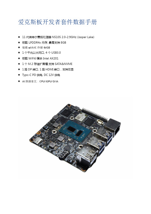
爱克斯板开发者套件数据手册说明书
规格书
概述 CPU GPU 内存 存储 存储扩展 BIOS 系统支持 推理单元 CPU iGPU GNA I/O 接口 以太网 USB 无线模组 电源输入
其他
显示
显示接口
英特尔赛扬 N5105 2.0-2.9GHz (formerly Jasper Lake) 英特尔 UHD 集成显卡 24 个执行单元 450MHz-800MHz 板载 LPDDR4x 2933MHz, 4GB/6GB/8GB 板载 64GB eMMC 存储 1 * M.2 Key-M 2242, Support SATA&NVME AMI UEFI BIOS Ubuntu Windows 10/11
85x85mm Operation: 0℃ - 45℃ Storage: -10℃ - 75℃ 5%~95% RH (non-condensing)
DC 12V Lower than 18W
1
Power
2
Headset & mic 2-in-1 3.5mm jack
3
Type-C PD Power Input
3
Type-C PD 电源输入
4
40-Pin GPIO 排针
5
RJ45 千兆以太网
6
USB3.0 Type-A x 2
7
USB3.0 Type-A x 2
8
DP x 1 , HDMI x1
9
DC 12V 输入板载 1.25mm 接口
10
M.2 2242 存储扩展
关键组件
尺寸
AIxBoard Edge Developer Kit Datasheet
Key Components
Dimensions
- 1、下载文档前请自行甄别文档内容的完整性,平台不提供额外的编辑、内容补充、找答案等附加服务。
- 2、"仅部分预览"的文档,不可在线预览部分如存在完整性等问题,可反馈申请退款(可完整预览的文档不适用该条件!)。
- 3、如文档侵犯您的权益,请联系客服反馈,我们会尽快为您处理(人工客服工作时间:9:00-18:30)。
M P A N Y C O N F I D E N T I A L C O M P A N Y C O N F I D E N T I A L C O M CCT/MB400-2.0STB5105-MBoardSchematicsDocument number: 7647937ECONTROLLED DOCUMENTAuthor: Mark BrowningMCDT BoardsLast saved: October 15, 2004DOCUMENT 7647937REVISION E CONTROLLED DOCUMENT (Check latest revision)DATE 19-OCT-2004page: 1/23M P A N Y C O N F I D E N T I A L C O M P A N Y C O N F I D E N T I A L C O M1 Modification History 1 Modification HistoryNOTE: Change bars at the edge of each page show changes between revisions of document.Please note that section 1Modification History,should only be used as a guide to the document changes and the whole document should be referenced for complete changes.Revision A7647937A: Created: 19th of April 2004 by Mark Browning. First draft for initial review.Revision B7647937B:Updated:8th of June 2004by Mark Browning.Updates following schematic review and design changes. This version to be reviewed externally.Revision C 7647937C:Updated:10th of August 2004by Mark Browning.Imported new STB5105pinout.PIO assignments for DVBCI IORD/IOWR signals changed to PIO3-5 and PIO3-6. Some other minor corrections made.Revision D7647937D:Updated:1st of September 2004by Mark Browning.New schematics reflect shipped Rev.A PCB.Added pull up/down option resistors to FMI address 22&23,added pull-down resistors to NIM transport stream control signals. Some other minor cosmetic changes made.Revision E 7647937E:Updated:6th of October 2004by Mark Browning.Schematics updated for Rev.B PCB.Schematic changes are as follows:•STB5105 pin out (map file) changes to reflect last minute pad-ring changes of the device.•In DVBCI block,notDVB_REG signal is now derived from FMI ADDR(15)and inverted as requested in DDTS GNBvd26698.•Fixed RS232-ASC0 signals that were swapped, see DDTS INSbl22790.•Changed values of resistors and capacitors associated with the 27MHz crystal,see DDTS INSbl22796•Changed values of DVBCI control strobe pull-up resistors to 10K Ohm.M P A N Y C O N F I D E N T I A L C O M P A N Y C O N F I D E N T I A L C O M2 Contents 2ContentsSectionDescription Page 1Modification History (22)Contents (33)MB400B Schematics ............................................................................. 33.1STB5105-MBoard (Top Sheet 1 of 6) - LMI ........................................... 43.2STB5105-MBoard (Top Sheet 2 of 6) - FMI ........................................... 53.3STB5105-MBoard (Top Sheet 3 of 6) - PIO ........................................... 63.4STB5105-MBoard (Top Sheet 4 of 6) - Audio & Video ........................ 73.5STB5105-MBoard (Top Sheet 5 of 6) - System & clocks .................... 83.6STB5105-MBoard (Top Sheet 1 of 6) - Powers .................................... 93.7STB5105-MBoard - LMI DDR SDRAM ................................................. 103.8STB5105-MBoard - FMI peripherals ................................................... 113.9STB5105-MBoard - STEM-EMI buffers ............................................... 123.10STB5105-MBoard - STEM-EMI connector .......................................... 133.11STB5105-MBoard - STEM-IO connector (unused)............................ 143.12STB5105-MBoard - DVBCI ................................................................... 153.13STB5105-MBoard - FMI FLASH ........................................................... 163.14STB5105-MBoard - Single ST -NIM connector .................................... 173.15STB5105-MBoard - Transport Stream buffers ................................... 183.16STB5105-MBoard - Single SMARTCARD connector ........................ 193.17STB5105-MBoard - RS232 serial ports .............................................. 203.18STB5105-MBoard - Infra Red .............................................................. 213.19STB5105-MBoard - Audio outputs (22)3.20STB5105-MBoard - Video outputs ...................................................... 233MB400B Schematics STB5105-MBoard schematics.M P A N Y C O N F I D E N T I A L C O M P A N Y C O N F I D E N T I A L C O MM P A N Y C O N F I D E N T I A L C O M P A N Y C O N F I D E N T I A L C O MM P A N Y C O N F I D E N T I A L C O M P A N Y C O N F I D E N T I A L C O MMP AN YCON FI DE NT IA LCOM P A N YCON FI D E N TI A LC O M3.4 STB5105-MBoard (Top Sheet 4 of 6) - Audio & VideoMP AN YCON FI DE NT IA LCOM P A N YCON FI D E N TI A LC O M3.5 STB5105-MBoard (Top Sheet 5 of 6) - System & clocksMP AN YCON FI DE NT IA LCOM P A N YCON FI D E N TI A LC O M3.6 STB5105-MBoard (Top Sheet 1 of 6) - PowersMP AN YCON FI DE NT IA LCOM P A N YCON FI D E N TI A LC O M3.7 STB5105-MBoard - LMI DDR SDRAMMP AN YCON FI DE NT IA LCOM P A N YCON FI D E N TI A LC O M3.8 STB5105-MBoard - FMI peripheralsMP AN YCON FI DE NT IA LCOM P A N YCON FI D E N TI A LC O M3.9 STB5105-MBoard - STEM-EMI buffersMP AN YCON FI DE NT IA LCOM P A N YCON FI D E N TI A LC O M3.10 STB5105-MBoard - STEM-EMI connectorMP AN YCON FI DE NT IA LCOM P A N YCON FI D E N TI A LC O M3.11 STB5105-MBoard - STEM-IO connector (unused)MP AN YCON FI DE NT IA LCOM P A N YCON FI D E N TI A LC O M3.12 STB5105-MBoard - DVBCIMP AN YCON FI DE NT IA LCOM P A N YCON FI D E N TI A LC O M3.13 STB5105-MBoard - FMI FLASHMP AN YCON FI DE NT IA LCOM P A N YCON FI D E N TI A LC O M3.14 STB5105-MBoard - Single ST-NIM connectorMP AN YCON FI DE NT IA LCOM P A N YCON FI D E N TI A LC O M3.15 STB5105-MBoard - Transport Stream buffersMP AN YCON FI DE NT IA LCOM P A N YCON FI D E N TI A LC O M3.16 STB5105-MBoard - Single SMARTCARD connectorMP AN YCON FI DE NT IA LCOM P A N YCON FI D E N TI A LC O M3.17 STB5105-MBoard - RS232 serial portsMP AN YCON FI DE NT IA LCOM P A N YCON FI D E N TI A LC O M3.18 STB5105-MBoard - Infra RedMP AN YCON FI DE NT IA LCOM P A N YCON FI D E N TI A LC O MMP AN YCON FI DE NT IA LCOM P A N YCON FI D E N TI A LC O M。