cadence信号完整性仿真步骤
信号完整性仿真流程
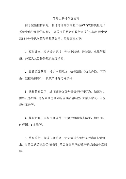
信号完整性仿真流程
信号完整性仿真是一种通过计算机辅助工程(CAE)软件模拟电子系统中信号质量的过程,主要关注的是高速数字信号在传输过程中受到的各种干扰对信号质量的影响。
简要流程如下:
1. 模型建立:根据设计需求,创建电路板、连接器、电缆等模型,并定义元器件参数及互连结构。
2. 设置边界条件:设定电源网络、信号激励(如上升沿、下降沿、数据眼图等)、负载条件等边界条件。
3. 选择仿真类型:进行瞬态仿真分析信号时域行为,如延时、振铃、过冲等;进行频域仿真分析信号频谱特性,如插入损耗、串扰、反射系数等。
4. 执行仿真:运行仿真软件,计算并输出仿真结果,如眼图、时序图、S参数等。
5. 结果分析:解读仿真结果,评估信号完整性是否满足设计要求,如是否满足建立保持时间、是否存在严重的噪声干扰或信号衰减等。
6. 优化设计:根据仿真结果对设计方案进行优化调整,如调整布线拓扑、添加端接电阻、优化电源/地平面布局等,然后再进行仿真验证,直至满足信号完整性要求。
cadence信号完整性仿真步骤.

IntroductionConsider the proverb, “It takes a village to raise a child.” Similarly, multiple design team members participate in assuring PCB power integrity (PI as a design moves from the early concept phase to becoming a mature product. On the front end, there’s the electrical design engineer who is responsible for the schematic. On the back end, the layout designer handles physical implemen-tation. Typically, a PI analysis expert is responsible for overall PCB PI and steps in early on to guide the contributions of others. How quickly a team can assure PCB PI relates to the effectiveness of that team. In this paper, we will take a look at currently popular analysis approaches to PCB PI. We will also introduce a team-based approach to PCB PI that yieldsadvantages in resource utilization and analysis results.Common Power Integrity Analysis MethodsThere are two distinct facets of PCB PI – DC and AC. DC PI guarantees thatadequate DC voltage is delivered to all active devices mounted on a PCB (oftenusing IR drop analysis. This helps to assure that constraints are met for currentdensity in planar metals and total current of vias and also that temperatureconstraints are met for metals and substrate materials. AC PI concerns thedelivery of AC current to mounted devices to support their switching activitywhile meeting constraints for transient noise voltage levels within the powerdelivery network (PDN. The PDN noise margin (variation from nominalvoltage is a sum of both DC IR drop and AC noise.DC PI is governed by resistance of the metals and the current pulled from thePDN by each mounted device. Engineers have, for many years, applied resistivenetwork models for approximate DC PI analysis. Now that computer speedsare faster and larger addressable memory is available, the industry is seeingmuch more application of layout-driven detailed numerical analysis techniquesfor DC PI. Approximation occurs less, accuracy is higher, and automation ofHow a Team-Based Approach to PCB Power Integrity Analysis Yields Better ResultsBy Brad Brim, Sr. Staff Product Engineer, Cadence Design SystemsAssuring power integrity of a PCB requires the contributions of multiple design team members. Traditionally, such an effort has involved a time-consuming process for a back-end-focused expert at the front end of a design. This paper examines a collaborative team-based approach that makes more efficient use of resources and provides more impact at critical points in the design process.ContentsIntroduction . (1)Common Power IntegrityAnalysis Methods . (1)Applying a Team-Based Approachto Power Integrity Analysis . (3)Summary (6)For Further Information . (7)whole-design analysis and postprocessing results are commonly available commercially. In fact, DC PI analysis for PCB designs has become a “signoff” requirement for many OEMs. See Figure 1 (left for typical results for current density.Since metal conductivity is temperature-dependent, DC IR drop is a nonlinear analysis. IR drop results can vary by more than 20% when temperature effects are considered, according to case studies for high-power designs. There is, however, a way to accurately characterize PCB IR drop wh ile assuring that the PDN noise margin isn’twasted. Using a DC analysis tool that provides capabilities such as electrical/thermal co-simulation, perform a linear electrical analysis at ambient temperature; take the resulting power loss and apply it to perform a linear thermal analysis. Then, perform another linear electrical analysis with consideration of the localized temperature-dependent conductivity. This process converges in just a few iterations to yield a desired result. See Figure 1 for an illustration of this solution, as implemented in the Cadence® Sigrity™ PowerDC™DC analysis tool.TemperatureLoss DensityPlane CurrentSurface TemperatureElectrical AnalysisThermal AnalysisFigure 1: Current density (left and temperature distribution (right for a PCB design due to DC powerdelivery as two linear solutions are iteratively linked to address nonlinear electro-thermal analysis.AC PI is governed by voltage regulator modules, loop inductances, decoupling capacitors (decaps, and plane capacitance. AC PI effects tend to be global in nature dueto plane resonances, plane-to-plane coupling, and shared reference planes. As such, this calls for full-board analysis, as well as more resource-intensive analysis algorithms. A hybrid of circuit theory and electromagnetic (EM analyses is the most commonly applied AC PI analysis for PCBs. This type of analysis is available in the frequency domain to extract S-parameters, using a tool such as Cadence Sigrity PowerSI™ frequency-domain electrical analysis solution. It’s also available in the time domain to directly generate transient waveforms, using a tool such as Cadence Sigrity Speed2000™ time-domain analysis solution. With the proper tools, an engineer can, in tens of minutes, accurately characterize the PDNbehavior of even the largest and most complex PCBs from DC to multi-gigahertz using single- to low double-digit gigabytes of memory.Transient PI analysis may seem attractive because it directly yields noise waveforms; however, in reality, it is less commonly applied than frequency-domain impedance analysis. “Target impedance” profiles are applied as PIconstraints. Lower impedance corresponds to lower transient noise. Without direct vendor specification, reasonable target impedance may be estimated based on device specifications for voltage ripple and AC switching current. See Figure 2 for a comparison of frequency-domain and time-domain results. In this comparison, the Cadence Sigrity OptimizePI ™ tool was used to significantly reduce an impedance peak near 800MHz by applying an alternate set of decaps to mount for a DIMM module. This solution reduced peak-to-peak PDN noise for the optimized design by 12% and the component and manufacturing cost of the decap implementation by 21%. 2How a Team-Based Approach to PCB Power Integrity Analysis Yields Better ResultsFigure 2: Impedance profile and transient PDN noise of a DIMM before and after thedecap implementation was optimized.Applying a Team-Based Approach to Power Integrity AnalysisTraditionally, PI experts have performed pre-layout decap selections and initial IR drop analyses. This is a substantial time investment at the front end of a design for a back-end-focused expert. By applying a more collaborativeapproach, a design team can make better use of its resources and expertise, and generate more impactful results.A team could set up simple analyses that yield actionable results and that could be performed by other members of the PI team. This PCB PI team would ideally consist ofthree key members: design engineer, layout designer, and PI analysis expert, as shown in Figure 3.Design Engineer•Can start with either BOM or schematic•Apply Power Feasibility Editor for DeCapselection and PIconstraint definitionLayout Designer•Can start as early as floorplanning stage •First order analysis directly on layout•Analyze, edit, re-analyze•DeCap placement guidanceand DRCPI Analysis Expert•Can start at any stage•Leverages setup and data from rest of team•Signoff capable detailed analysis Figure 3: Roles and responsibilities of the PCB PI design team. 3How a Team-Based Approach to PCB Power Integrity Analysis Yields Better ResultsThere is now a tool available on the market that supports team-based PCB PI analysis. Cadence A llegro® Sigrity PI is the industry’s first front-to-back, constraint-based PI approach for PCB and IC package designs. This tool differs from other solutions in the way that it accesses existing analysis algorithms and how the analysis results are applied. In addition, the tool also provides PI-focused infrastructure support of non-analysis tasks. As a result, design engineers and layout designers can contribute earlierand more effectively to PCB PI. The DC and AC PI analysis capabilities described in the previous section are available in the associated Power Integrity Signoff and Optimization Option.PCB design engineers are responsible for front-end tasks. They must generate an initial Bill of Materials (BOM to set in motion cost feasibility studies and assure electrical design intent by generating circuit schematics. They typically work independently of DC PI concerns. However, to support AC PI, design engineers must add decaps and include them in the BOM and the schematic. Some device vendors provide datasheet guidance for decap selection (type and/or quantity, but many do not. Even with datasheet guidance, it is tedious for design engineers toassemble and interpret the specifications for each device, instantiate all the unique components, assure they appear logically in the schematic, etc. No mechanism has existed for physical placement guidance to be communicated for back-end application.With constraint-based design methods, engineers gain a uniform interface for design-intent information and for automating a broad class of tasks across front-to-back flows. PI [electrical] constraint sets (PI Csets have been added to save all component-level PI information. Design engineers may apply PI Csets to quickly and completely define PI design intent for all mounted components. PI Csets also automate instantiation of components and inclusion in the BOM.Refer to Figure 4 for an example of a PI Cset in Allegro Sigrity PI. PI Csets contain information for each power rail,including decap component names, quantity of each component, package type, and physical placement guidance.Figure 4: PI constraint set contents viewed from the constraint manager.PI Cset creation is automated by the tool’s Power Feasibility Editor, which providesa mechanism to enter datasheet decap selection and physical placement guidance. Figure5 shows a view of the tool’s Power Feasibility Editor. In addition to placement guidance,a PI Cset communicates to the layout designer component and power rail associ-ation for decaps, helping the designer perform more reliable placement. 4How a Team-Based Approach to PCB Power Integrity Analysis Yields Better ResultsFigure 5: Single-point analysis results in the Power Feasibility Editor.The Power Feasibility Editor also provides access to approximate and detailed pre-layout analysis for selection and placement of decaps. High-level specifications are made to generate target impedance profiles when device vendors do not provide them. An approximate PI analysis called “single-point” is provided for interactive decap selection. For more detailed pre-layout, the tool provides access to the data in the Cadence Sigrity OptimizePI tool.The engineer simply clicks a button within the Power Feasibility Editor to generate PI Csets.Figure 6: Split-screen view of layout (left and IR drop analysis results (right.Unlike design engineers, layout designers are concerned with DC PI issues. Layout designers control metal shapes and vias and these, in turn, control PI behaviors for DC IR drop and current flow. Layout designers can intuitively understand and act upon analysis results for these DC PI effects. The Allegro Sigrity PI tool provides access within the layout environment to the setup and results display for DC IR drop and current constraint analyses. DC analysis is fast, though not conducted in real time in order to enable dynamic updating of analysis results as layout updates are made. 5How a Team-Based Approach to PCB Power Integrity Analysis Yields Better ResultsHow a Team-Based Approach to PCB Power Integrity Analysis Yields Better Results The tool provides a split-screen view, as shown in Figure 6, to support a fixedview of analysis results as layout designers dynamically make updates to address IR drop or current constraint issues. The two views are synchronized for operations that affect the display, such as layer changes, zoom, and pan. Layout designers can apply this split-screen view of DC analysis results as they craft an initial layout, before the PI analysis expert gets involved. As a more effective method to communicate where PI issues exist in the design, the split-screen view can also be applied with detailed analysis results performed separately by PI analysis experts. In fact, to more quickly verify improved PI performance, the layout designer can launch the same detailed analysis performed by the PI analyst. Layout designers strongly influence AC PI success with their placement of decaps. Decaps placed close to a device generally benefit PI, but restrict routing channels due to decap mounting vias. Decaps placed too far from a device will be ineffective at providing switching current to the device and will negatively affect PI. Present design methods do not typically provide decap placement guidance, including information as simple as which device is associated with a decap. By conveying design intent, previously described PI Csets enable more effective placement of decaps by layout designers. The associated device and power rail and placement guidance are all specified in the PI Cset. A decap placement mode is implemented to support layout designers, as shown in Figure 7. Simply select a mounted component and a power rail, and then cycle through a point-and-click placement process. The selected device is highlighted and three optional visual placement guidance displays are available: device to decap distance for top layer, device to decap distance for bottom layer, and decap effective radius. The first two are defined in the PI Cset and are conceptually familiar. The decap effective radius is the maximum distance at which the decap will be maximally effective. It is a function of the stack-up and decap mounting parasitics as well as the decap value and its intrinsic parasitics. It is dynamically computed as the cursor moves due to local availability of metal shapes on the associated power and ground layers. Decap Placement Guidance Top-side Setback Distance * Decap Effective Radius Bottom-side Setback Distance Figure 7: Layout view during decap placement for device U0501 with top (yellow andbottom (blue setback distances and decap effective radius (white circle displayed To ease the setup for detailed PI analysis, design intent and analysis setup information specified by design engineers and layout designers is available to PI analysis. PI Csets serve as a convenient mechanism to communicate updated placement guidance or requirements for updates on decap selection (either type or quantity for a specific device instance or all devices to which a PI Cset is applied. Changes to PI Csets also convey information back to the design engineer and enable automated update of the schematic and BOM. Summary While current PCB PI analysis tools are continuing to serve the design community well, they are even more effective when combined with a front-to-back, constraint-based approach. Under this type of methodology, each design team member can more efficiently accomplish his or her individual tasks and communicate design intent information to colleagues for increased efficiency of the overall PCB design flow. This approach provides access to 6How a Team-Based Approach to PCB Power Integrity Analysis Yields Better Results actionable analysis results where they are most impactful. It also leverages earlier defined analysis setup information for the PI expert, and eases communication of design changes from his or her back-end role to front-end colleagues. For Further Information To learn more about Cadence Allegro Sigrity PI solution, visit:/products/sigrity/Pages/ solution.aspx Cadence Design Systems enables global electronic design innovation and plays an essential role in the creation of today’s electronics. Customers use Cadence software, hardware, IP, and expertise to design and verify to day’s mobile, cloud and connectivity applications. © 2014 Cadence Design Systems, Inc. All rights reserved. Cadence, the Cadence logo, and Allegro are registered trademarks and OptimizePI, PowerDC, PowerSI, Sigrity, and Speed2000 are trademarks of Cadence Design Systems, Inc. All others are properties of their respective holders. 1932 01/14 CY/DM/PDF。
CADENCE仿真流程
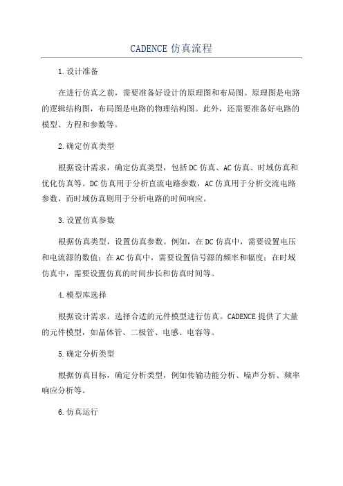
CADENCE仿真流程1.设计准备在进行仿真之前,需要准备好设计的原理图和布局图。
原理图是电路的逻辑结构图,布局图是电路的物理结构图。
此外,还需要准备好电路的模型、方程和参数等。
2.确定仿真类型根据设计需求,确定仿真类型,包括DC仿真、AC仿真、时域仿真和优化仿真等。
DC仿真用于分析直流电路参数,AC仿真用于分析交流电路参数,而时域仿真则用于分析电路的时间响应。
3.设置仿真参数根据仿真类型,设置仿真参数。
例如,在DC仿真中,需要设置电压和电流源的数值;在AC仿真中,需要设置信号源的频率和幅度;在时域仿真中,需要设置仿真的时间步长和仿真时间等。
4.模型库选择根据设计需求,选择合适的元件模型进行仿真。
CADENCE提供了大量的元件模型,如晶体管、二极管、电感、电容等。
5.确定分析类型根据仿真目标,确定分析类型,例如传输功能分析、噪声分析、频率响应分析等。
6.仿真运行在仿真运行之前,需要对电路进行布局和连线。
使用CADENCE提供的工具对电路进行布局和连线,并生成物理设计。
7.仿真结果分析仿真运行后,CADENCE会生成仿真结果。
利用CADENCE提供的分析工具对仿真结果进行分析,观察电路的性能指标。
8.优化和修改根据仿真结果,对电路进行优化和修改。
根据需要,可以调整电路的拓扑结构、参数和模型等,以改进电路的性能。
9.再次仿真和验证根据修改后的电路,再次进行仿真和验证,以确认电路的性能指标是否得到改善。
最后需要注意的是,CADENCE仿真流程并不是一成不变的,根据具体的设计需求和仿真目标,流程可能会有所调整和修改。
此外,CADENCE还提供了许多其他的工具和功能,如电路板设计、封装设计、时序分析等,可以根据需要进行使用。
Cadence SI信号完整性仿真技术
Cadence PCB SI仿真流程——孙海峰高速高密度多层PCB板的SI/EMC(信号完整性/电磁兼容)问题长久以来一直是设计者所面对的最大挑战。
然而,随着主流的MCU、DSP和处理器大多工作在100MHz以上(有些甚至工作于GHz级以上),以及越来越多的高速I/O埠和RF前端也都工作在GHz级以上,再加上应用系统的小型化趋势导致的PCB 空间缩小问题,使得目前的高速高密度PCB板设计已经变得越来越普遍。
许多产业分析师指出,在进入21世纪以后,80%以上的多层PCB设计都将会针对高速电路。
高速讯号会导致PCB板上的长互连走线产生传输线效应,它使得PCB设计者必须考虑传输线的延迟和阻抗搭配问题,因为接收端和驱动端的阻抗不搭配都会在传输在线产生反射讯号,而严重影响到讯号的完整性。
另一方面,高密度PCB板上的高速讯号或频率走线则会对间距越来越小的相邻走线产生很难准确量化的串扰与EMC问题。
SI和EMC的问题将会导致PCB设计过程的反复,而使得产品的开发周期一再延误。
一般来说,高速高密度PCB需要复杂的阻抗受控布线策略才能确保电路正常工作。
随着新型组件的电压越来越低、PCB板密度越来越大、边缘转换速率越来越快,以及开发周期越来越短,SI/EMC挑战便日趋严峻。
为了达到这个挑战的要求,目前的PCB设计者必须采用新的方法来确保其PCB设计的可行性与可制造性。
过去的传统设计规则已经无法满足今日的时序和讯号完整性要求,而必须采取包含仿真功能的新款工具才足以确保设计成功。
Cadence的Allegro PCB SI提供了一种弹性化且整合的信号完整性问题解决方案,它是一种完整的SI/PI(功率完整性)/EMI问题的协同解决方案,适用于高速PCB设计周期的每个阶段,并解决与电气性能相关的问题。
Allegro PCB SI信号完整性分析的操作步骤,就是接下来将要介绍的。
一、Allegro PCB SI分析前准备:1、准备需要分析的PCB,如下图;2、SI分析前的相关设置,执行T ools/Setup Advisor,进入Database Setup Advisor 对话框,进行SI分析前的设置;(1)设置PCB叠层的材料、阻抗等,点击Edit Cross section,进入叠层阻抗等设置界面。
CADENCE仿真步骤
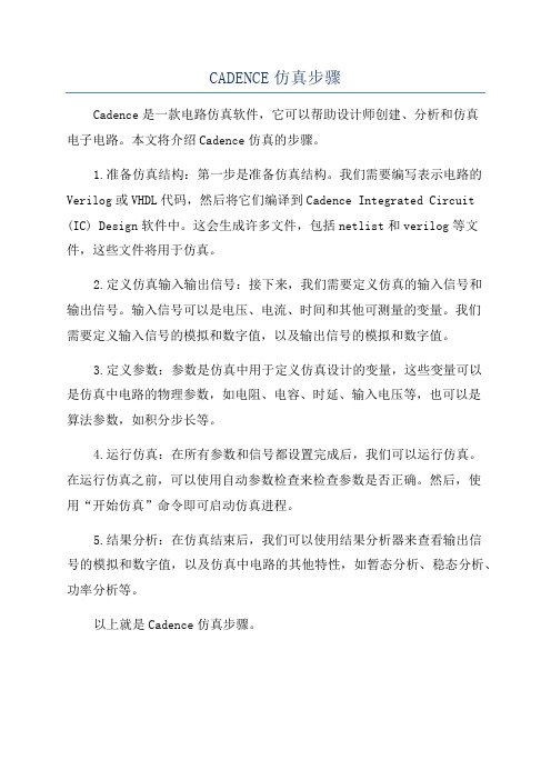
CADENCE仿真步骤
Cadence是一款电路仿真软件,它可以帮助设计师创建、分析和仿真
电子电路。
本文将介绍Cadence仿真的步骤。
1.准备仿真结构:第一步是准备仿真结构。
我们需要编写表示电路的Verilog或VHDL代码,然后将它们编译到Cadence Integrated Circuit (IC) Design软件中。
这会生成许多文件,包括netlist和verilog等文件,这些文件将用于仿真。
2.定义仿真输入输出信号:接下来,我们需要定义仿真的输入信号和
输出信号。
输入信号可以是电压、电流、时间和其他可测量的变量。
我们
需要定义输入信号的模拟和数字值,以及输出信号的模拟和数字值。
3.定义参数:参数是仿真中用于定义仿真设计的变量,这些变量可以
是仿真中电路的物理参数,如电阻、电容、时延、输入电压等,也可以是
算法参数,如积分步长等。
4.运行仿真:在所有参数和信号都设置完成后,我们可以运行仿真。
在运行仿真之前,可以使用自动参数检查来检查参数是否正确。
然后,使
用“开始仿真”命令即可启动仿真进程。
5.结果分析:在仿真结束后,我们可以使用结果分析器来查看输出信
号的模拟和数字值,以及仿真中电路的其他特性,如暂态分析、稳态分析、功率分析等。
以上就是Cadence仿真步骤。
利用CadenceAllegro进行PCB级的信号完整性仿真

收稿日期:2002-04-03利用Cadence A llegro进行PCB级的信号完整性仿真Signa l I n tegr ity Si m ula tion w ith A llegro for PCB Board D esign李 新L i X in 张 琳Zhang L in(西安电子科技大学 西安 710071) (西安大唐电信有限公司 西安 710075)(X idian U niversity,X i′an,710071,Ch ina) (X i′an D atang Telecom,X i′an,710075,Ch ina)摘 要 在高速PCB设计过程中,仅仅依靠个人经验布线,往往存在巨大的局限性。
利用Cadence的A llegro软件包对电路进行PCB级的仿真,可以最优化线路布局,极大地提高电路设计质量,从而缩短设计周期。
本文结合作者的实际设计经验,介绍使用Cadence的一般步骤并列举在使用过程中所发现的一些问题。
关键词 高速PCB布线 A llegro文件转换 信号完整性仿真 随着信息宽带化和高速化的发展,以前的低速PCB已完全不能满足日益增长信息化发展的需要,而高速PCB的出现将对硬件人员提出更高的要求,仅仅依靠自己的经验去布线,会顾此失彼,造成研发周期过长,浪费财力物力,生产出来的产品不稳定。
一般认为高速PCB是指其数字信号边沿上升时间小于4倍信号传输时延,这种高速PCB的信号线必须按照传输线理论去设计,否则将会严重影响信号的完整性。
Cadence公司针对PCB D esign Studi o发布一个功能非常实用的高速电路设计及信号完整性分析的工具选件ALL EGRO PCB。
利用这个仿真软件能够根据叠层的排序,PCB的介电常数,介质的厚度,信号层所处的位置以及线宽等等来判断某一PCB线条是否属于微带线、带状线、宽带耦合带状线,并且根据不同的计算公式自动计算出信号线的阻抗以及信号的反射、串绕、电磁干扰等等,从而可以对布线进行约束以保证PCB的信号完整性。
电路板级的信号完整性问题和仿真分析

电路板级的信号完整性问题和仿真分析摘要:今天随着电子技术的发展,电路板设计中的信号完整性问题已成为PCB设计者必须面对的问题。
信号完整性指的是什么?信号在电路中传输的质量。
由于电子产品向高速、微型化的发展,导致集成电路开关速度的加快,产生了信号完整性问题。
常见的问题有反弹、振铃、地弹和串扰等等。
这些问题将会对电路板设计产生怎样的影响?通过理论分析探讨,找到解决它们的一些途径。
传统的PCB设计是在样机中去测试问题,极大的降低了产品设计的效率。
使用EDA工具分析,可以将问题在计算机中进行暴露处理,降低问题的出现,提高产品的设计效率。
这里以Altium Designer 6.0工具为例,介绍分析解决部分信号完整性问题的方法。
关键词:信号完整性 Altium Designer 6.0 仿真分析[中图分类号] O59 [文献标识码] A [文章编号] 1000-7326(2012)04-0125-0320世纪初叶,科学家先后发明了真空二极管和三极管,它代表人类进入了电子技术时代。
随后半导体晶体管和集成电路的出现,将电子技术推向了一个新的时期。
特别是IC芯片的发展,使电子产品越来越趋向于小型化、高速化、数字化。
但同时却给电子设计带来一个新的问题:体积减小导致电路的布局布线密度变大,而同时信号的频率也在迅速提高,如何处理越来越快的信号。
这就是我们硬件设计中遇到的最核心问题:信号完整性。
为什么我们以前在学校学习和电子制作中没有遇到呢?那是因为在模拟电路中,采用的是单频或窄频带信号,我们关心的只是电路的信噪比,没有去考虑信号波形和波形畸变;而在数字电路中,电平跳变的信号上升时间比较长,一般为几个纳秒。
元件间的布线不会影响电路的信号,所以都没有去考虑信号完整性问题。
但是今天,随着GHz时代的到来,很多IC的开关速度都在皮秒级别,同时由于对低功耗的追求,芯片内核电压越来越低,电子系统所能容忍的噪声余量越来越小,那么电路设计中的信号完整性问题就突现出来了。
cadence原理图仿真
cadence原理图仿真
在进行Cadence原理图仿真时,我们需要注意以下几点,以确保仿真结果的准确性和可靠性:
1. 确认所使用的元件符合仿真要求,并正确地添加到原理图中。
这包括在仿真库中选择合适的元件模型,并将其与其他元件正确地连接起来。
2. 确认仿真的电源和接地连接正确无误。
确保电源和地线的连接不会导致任何不良影响,如电压下降或噪声干扰。
3. 设置仿真参数,如仿真时间、仿真步长等。
根据所需的仿真精度和仿真效率,选择适当的仿真参数。
4. 进行信号源的设置。
这包括选择合适的信号源类型(如AC
信号、脉冲信号等)、设置信号源的频率和振幅等参数。
5. 添加测量器件,以便在仿真过程中监测所需的电压或电流。
这些测量器件可以是电压表、电流表或示波器等。
6. 设置仿真分析类型。
根据需要进行直流分析、交流分析或者是时域分析等。
选择适当的仿真分析类型以获得所需的结果。
7. 运行仿真并分析结果。
运行仿真过程,等待仿真完成后,通过分析仿真结果来获取我们所需的电压、电流或其他信号参数。
通过遵循以上步骤,我们可以在Cadence中进行原理图仿真,并获取准确可靠的仿真结果,以验证电路设计的正确性和性能。
- 1、下载文档前请自行甄别文档内容的完整性,平台不提供额外的编辑、内容补充、找答案等附加服务。
- 2、"仅部分预览"的文档,不可在线预览部分如存在完整性等问题,可反馈申请退款(可完整预览的文档不适用该条件!)。
- 3、如文档侵犯您的权益,请联系客服反馈,我们会尽快为您处理(人工客服工作时间:9:00-18:30)。
IntroductionConsider the proverb, “It takes a village to raise a child.” Similarly, multiple design team members participate in assuring PCB power integrity (PI) as a design moves from the early concept phase to becoming a mature product. On the front end, there’s the electrical design engineer who is responsible for the schematic. On the back end, the layout designer handles physical implemen-tation. Typically, a PI analysis expert is responsible for overall PCB PI and steps in early on to guide the contributions of others. How quickly a team can assure PCB PI relates to the effectiveness of that team. In this paper, we will take a look at currently popular analysis approaches to PCB PI. We will also introduce a team-based approach to PCB PI that yieldsadvantages in resource utilization and analysis results.Common Power Integrity Analysis MethodsThere are two distinct facets of PCB PI – DC and AC. DC PI guarantees thatadequate DC voltage is delivered to all active devices mounted on a PCB (oftenusing IR drop analysis). This helps to assure that constraints are met for currentdensity in planar metals and total current of vias and also that temperatureconstraints are met for metals and substrate materials. AC PI concerns thedelivery of AC current to mounted devices to support their switching activitywhile meeting constraints for transient noise voltage levels within the powerdelivery network (PDN). The PDN noise margin (variation from nominalvoltage) is a sum of both DC IR drop and AC noise.DC PI is governed by resistance of the metals and the current pulled from thePDN by each mounted device. Engineers have, for many years, applied resistivenetwork models for approximate DC PI analysis. Now that computer speedsare faster and larger addressable memory is available, the industry is seeingmuch more application of layout-driven detailed numerical analysis techniquesfor DC PI. Approximation occurs less, accuracy is higher, and automation ofHow a Team-Based Approach to PCB Power Integrity Analysis Yields Better ResultsBy Brad Brim, Sr. Staff Product Engineer, Cadence Design SystemsAssuring power integrity of a PCB requires the contributions of multiple design team members. Traditionally, such an effort has involved a time-consuming process for a back-end-focused expert at the front end of a design. This paper examines a collaborative team-based approach that makes more efficient use of resources and provides more impact at critical points in the design process.ContentsIntroduction (1)Common Power IntegrityAnalysis Methods (1)Applying a Team-Based Approachto Power Integrity Analysis (3)Summary (6)For Further Information (7)whole-design analysis and postprocessing results are commonly available commercially. In fact, DC PI analysis for PCB designs has become a “signoff” requirement for many OEMs. See Figure 1 (left) for typical results for current density.Since metal conductivity is temperature-dependent, DC IR drop is a nonlinear analysis. IR drop results can vary by more than 20% when temperature effects are considered, according to case studies for high-power designs. There is, however, a way to accurately characterize PCB IR drop while assuring that the PDN noise margin isn’twasted. Using a DC analysis tool that provides capabilities such as electrical/thermal co-simulation, perform a linear electrical analysis at ambient temperature; take the resulting power loss and apply it to perform a linear thermal analysis. Then, perform another linear electrical analysis with consideration of the localized temperature-dependent conductivity. This process converges in just a few iterations to yield a desired result. See Figure 1 for an illustration of this solution, as implemented in the Cadence ® Sigrity ™ PowerDC ™DC analysis tool.TemperatureLoss DensityPlane Current Surface TemperatureElectrical Analysis Thermal AnalysisFigure 1: Current density (left) and temperature distribution (right) for a PCB design due to DC powerdelivery as two linear solutions are iteratively linked to address nonlinear electro-thermal analysis.AC PI is governed by voltage regulator modules, loop inductances, decoupling capacitors (decaps), and plane capacitance. AC PI effects tend to be global in nature due to plane resonances, plane-to-plane coupling, and shared reference planes. As such, this calls for full-board analysis, as well as more resource-intensive analysis algorithms. A hybrid of circuit theory and electromagnetic (EM) analyses is the most commonly applied AC PI analysis for PCBs. This type of analysis is available in the frequency domain to extract S-parameters, using a tool such as Cadence Sigrity PowerSI ™ frequency-domain electrical analysis solution. It’s also available in the time domain to directly generate transient waveforms, using a tool such as Cadence Sigrity Speed2000™ time-domain analysis solution. With the proper tools, an engineer can, in tens of minutes, accurately characterize the PDNbehavior of even the largest and most complex PCBs from DC to multi-gigahertz using single- to low double-digit gigabytes of memory.Transient PI analysis may seem attractive because it directly yields noise waveforms; however, in reality, it is less commonly applied than frequency-domain impedance analysis. “Target impedance” profiles are applied as PIconstraints. Lower impedance corresponds to lower transient noise. Without direct vendor specification, reasonable target impedance may be estimated based on device specifications for voltage ripple and AC switching current. See Figure 2 for a comparison of frequency-domain and time-domain results. In this comparison, the Cadence Sigrity OptimizePI ™ tool was used to significantly reduce an impedance peak near 800MHz by applying an alternate set of decaps to mount for a DIMM module. This solution reduced peak-to-peak PDN noise for the optimized design by 12% and the component and manufacturing cost of the decap implementation by 21%.Figure 2: Impedance profile and transient PDN noise of a DIMM before and after thedecap implementation was optimized.Applying a Team-Based Approach to Power Integrity AnalysisTraditionally, PI experts have performed pre-layout decap selections and initial IR drop analyses. This is a substantial time investment at the front end of a design for a back-end-focused expert. By applying a more collaborative approach, a design team can make better use of its resources and expertise, and generate more impactful results.A team could set up simple analyses that yield actionable results and that could be performed by other members of the PI team. This PCB PI team would ideally consist of three key members: design engineer, layout designer, and PI analysis expert, as shown in Figure 3.Design Engineer•Can start with either BOM or schematic•Apply Power Feasibility Editor for DeCap selection and PIconstraint definitionLayout Designer•Can start as early asfloorplanning stage•First order analysis directlyon layout•Analyze, edit, re-analyze•DeCap placement guidanceand DRCPI Analysis Expert•Can start at any stage•Leverages setup and datafrom rest of team•Signoff capable detailedanalysisFigure 3: Roles and responsibilities of the PCB PI design team.There is now a tool available on the market that supports team-based PCB PI analysis. Cadence Allegro® SigrityPI is the industry’s first front-to-back, constraint-based PI approach for PCB and IC package designs. This tool differs from other solutions in the way that it accesses existing analysis algorithms and how the analysis resultsare applied. In addition, the tool also provides PI-focused infrastructure support of non-analysis tasks. As a result, design engineers and layout designers can contribute earlier and more effectively to PCB PI. The DC and AC PI analysis capabilities described in the previous section are available in the associated Power Integrity Signoff and Optimization Option.PCB design engineers are responsible for front-end tasks. They must generate an initial Bill of Materials (BOM)to set in motion cost feasibility studies and assure electrical design intent by generating circuit schematics. They typically work independently of DC PI concerns. However, to support AC PI, design engineers must add decaps and include them in the BOM and the schematic. Some device vendors provide datasheet guidance for decap selection (type and/or quantity), but many do not. Even with datasheet guidance, it is tedious for design engineers to assemble and interpret the specifications for each device, instantiate all the unique components, assure they appear logically in the schematic, etc. No mechanism has existed for physical placement guidance to be communicated for back-end application.With constraint-based design methods, engineers gain a uniform interface for design-intent information and for automating a broad class of tasks across front-to-back flows. PI [electrical] constraint sets (PI Csets) have been added to save all component-level PI information. Design engineers may apply PI Csets to quickly and completely define PI design intent for all mounted components. PI Csets also automate instantiation of components and inclusion in the BOM.Refer to Figure 4 for an example of a PI Cset in Allegro Sigrity PI. PI Csets contain information for each power rail, including decap component names, quantity of each component, package type, and physical placement guidance.Figure 4: PI constraint set contents viewed from the constraint manager.PI Cset creation is automated by the tool’s Power Feasibility Editor, which provides a mechanism to enter datasheet decap selection and physical placement guidance. Figure 5 shows a view of the tool’s Power Feasibility Editor. In addition to placement guidance, a PI Cset communicates to the layout designer component and power rail associ-ation for decaps, helping the designer perform more reliable placement.Figure 5: Single-point analysis results in the Power Feasibility Editor.The Power Feasibility Editor also provides access to approximate and detailed pre-layout analysis for selectionand placement of decaps. High-level specifications are made to generate target impedance profiles when device vendors do not provide them. An approximate PI analysis called “single-point” is provided for interactive decap selection. For more detailed pre-layout, the tool provides access to the data in the Cadence Sigrity OptimizePI tool. The engineer simply clicks a button within the Power Feasibility Editor to generate PI Csets.Figure 6: Split-screen view of layout (left) and IR drop analysis results (right).Unlike design engineers, layout designers are concerned with DC PI issues. Layout designers control metal shapes and vias and these, in turn, control PI behaviors for DC IR drop and current flow. Layout designers can intuitively understand and act upon analysis results for these DC PI effects. The Allegro Sigrity PI tool provides access within the layout environment to the setup and results display for DC IR drop and current constraint analyses. DC analysis is fast, though not conducted in real time in order to enable dynamic updating of analysis results as layout updates are made.The tool provides a split-screen view, as shown in Figure 6, to support a fixed view of analysis results as layout designers dynamically make updates to address IR drop or current constraint issues. The two views are synchro-nized for operations that affect the display, such as layer changes, zoom, and pan. Layout designers can apply this split-screen view of DC analysis results as they craft an initial layout, before the PI analysis expert gets involved.As a more effective method to communicate where PI issues exist in the design, the split-screen view can also be applied with detailed analysis results performed separately by PI analysis experts. In fact, to more quickly verify improved PI performance, the layout designer can launch the same detailed analysis performed by the PI analyst. Layout designers strongly influence AC PI success with their placement of decaps. Decaps placed close to a device generally benefit PI, but restrict routing channels due to decap mounting vias. Decaps placed too far from a device will be ineffective at providing switching current to the device and will negatively affect PI. Present design methods do not typically provide decap placement guidance, including information as simple as which device is associated with a decap. By conveying design intent, previously described PI Csets enable more effective placement of decaps by layout designers. The associated device and power rail and placement guidance are all specified in the PI Cset.A decap placement mode is implemented to support layout designers, as shown in Figure 7. Simply select a mounted component and a power rail, and then cycle through a point-and-click placement process. The selected device is highlighted and three optional visual placement guidance displays are available: device to decap distance for top layer, device to decap distance for bottom layer, and decap effective radius. The first two are defined in the PI Cset and are conceptually familiar. The decap effective radius is the maximum distance at which the decap will be maximally effective. It is a function of the stack-up and decap mounting parasitics as well as the decap value and its intrinsic parasitics. It is dynamically computed as the cursor moves due to local availability of metal shapes on the associated power and ground layers.Decap Placement GuidanceTop-sideSetbackDistance*DecapEffectiveRadiusBottom-sideSetbackDistanceFigure 7: Layout view during decap placement for device U0501 with top (yellow) and bottom (blue)setback distances and decap effective radius (white circle) displayedTo ease the setup for detailed PI analysis, design intent and analysis setup information specified by design engineers and layout designers is available to PI analysis. PI Csets serve as a convenient mechanism to communicate updated placement guidance or requirements for updates on decap selection (either type or quantity) for a specific device instance or all devices to which a PI Cset is applied. Changes to PI Csets also convey information back to the design engineer and enable automated update of the schematic and BOM.SummaryWhile current PCB PI analysis tools are continuing to serve the design community well, they are even more effective when combined with a front-to-back, constraint-based approach. Under this type of methodology, each design team member can more efficiently accomplish his or her individual tasks and communicate design intent infor-mation to colleagues for increased efficiency of the overall PCB design flow. This approach provides access toactionable analysis results where they are most impactful. It also leverages earlier defined analysis setup infor-mation for the PI expert, and eases communication of design changes from his or her back-end role to front-end colleagues.For Further InformationTo learn more about Cadence Allegro Sigrity PI solution, visit: /products/sigrity/Pages/ solution.aspxCadence Design Systems enables global electronic design innovation and plays an essential role in thecreation of today’s electronics. Customers use Cadence software, hardware, IP, and expertise to designand verify today’s mobile, cloud and connectivity applications. © 2014 Cadence Design Systems, Inc. All rights reserved. Cadence, the Cadence logo, and Allegro are registered trademarks and OptimizePI,PowerDC, PowerSI, Sigrity, and Speed2000 are trademarks of Cadence Design Systems, Inc. All others are properties of their respective holders.。