STM32F072调试软件详解
STM32调试方法
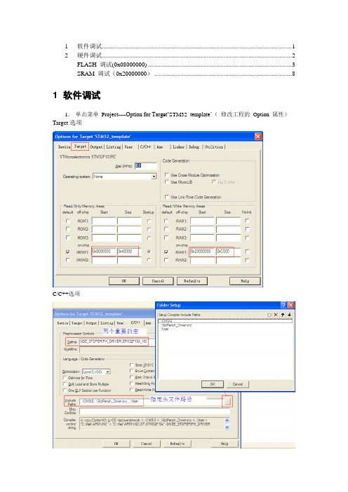
1 软件调试 (1)2 硬件调试 (2)FLASH 调试(0x08000000) (3)SRAM 调试(0x20000000) (8)1 软件调试1.单击菜单Project----Option for Target‘STM32_template’(修改工程的Option 属性)Target选项C/C++选项Debug选项(软件调试)2 硬件调试本文以STM32F103RC芯片为例,根据STM32F103RC Datasheet可知芯片的片内FLASH 基址为0x08000000,大小为256K(0x40000);片内RAM基址为0x20000000,大小为48K (0xc000)。
芯片启动模式如下:芯片的启动模式需要根据你程序下载的具体地址进行正确设置这里主要介绍两种硬件调试方法FLASH调试(程序下载到FLASH中,0x08000000)SRAM调试(程序下载到SRAM中,0x20000000)FLASH 调试(0x08000000)用JLink 连接好电脑跟实验箱,实验箱BOOT0接0(短路帽接上面两个引脚)�FLASH调试的参数设置1)单击菜单Project----Option for Target‘STM32_template’(修改工程的Option 属性)前面的选项跟软件调试设置一样,对下列选项进行配置:Debug 选项,选择调试工具选择“Settings”,见下图进入“Cortex JLink/JTrace Target Driver Setup”Debug 选项(默认)Trace选项(默认)Flash Download选项配置如下,点击“Add”选好之后,点击“Add”返回点击“OK”返回。
Utilities选项☒编译1.点击Project----> rebuild target files☒启动调试1.点击Debug ---> Start Debug 整个调试界面图,在调试窗口中可看到汇编代码的地址为0x0800开头,说明代码烧进到了FLASH中:点击全速运行,观察实验结果,调试完成。
【STM32H7教程】第5章STM32H7下载和调试方法(MDK5)

【STM32H7教程】第5章STM32H7下载和调试⽅法(MDK5)第5章 STM32H7下载和调试⽅法(MDK5)本章教程为⼤家介绍如何通过MDK5下载程序到芯⽚⾥⾯以及MDK5的调试和配置⽅法。
5.1 初学者重要提⽰5.2 使⽤MDK调试和下载程序设置(JLINK)5.3 使⽤MDK调试和下载程序设置(STLINK)5.4 MDK调试容易崩溃的解决办法5.5 MDK程序调试5.6 总结5.1 初学者重要提⽰1. 如果使⽤JLINK调试下载STM32H7,务必使⽤JLINK V9或V10,之前的版本已经不⽀持。
2. 如果使⽤STLINK调试下载STM32H7,推荐使⽤最新的电脑端驱动和对应的固件,详情见第2章的2.6⼩节。
3. MDK曾发布的STM32F1,F407,F429和F7的所有调试⽅法的设置细节及其注意事项,同样适⽤于STM32H7:。
4. MDK5调试过程中容易崩溃的问题,请看本章5.4⼩节,⽐较重要。
5. JLINK⽆法下载解决思路以及常见问题整理,适⽤于其它LINK:。
5.2 使⽤MDK调试和下载程序设置(JLINK)调试下载STM32H7,务必使⽤JLINK V9或V10,之前的版本已经不⽀持,JLINK的驱动安装等相关⽂件已经在本教程第2章的2.5章节有说明。
在上个章节⾥⾯,我们已经将Options对话框⾥⾯⼤部分设置选项都做了说明,本章节主要是调试下载的设置。
5.2.1 开发板和JLINK的接线图开发板接上JLINK的效果图如下,JLINK端需要插⼊开发板赠送的JTAG转SWD转接板:注意转接板不要插反了:5.2.2 设置Options⾥⾯的Debug选项Debug选项主要⽤于调试设置。
打开Settings设置选项,设置完毕后别忘了点击确定。
5.2.3 设置Options⾥⾯的Utilities选项Utilities选项主要⽤于程序下载设置。
5.2.4 程序下载前两步设置好之后,JLINK插到电脑端并跟开发板连接好,将板⼦上电,就可以下载了。
stm32f470的can2开发例程

一、介绍STMicroelectronics的STM32F470微处理器系列是一款性能强大的32位ARM Cortex-M4微控制器,具有丰富的外设和高度集成的特点。
其中,CAN2外设是其重要的通信接口之一,用于在汽车电子、工业控制和其它领域中实现可靠的数据传输。
本文将介绍如何在STM32F470微控制器上进行CAN2的开发,为读者提供完整的开发例程。
二、硬件准备在进行CAN2开发前,首先需要准备好硬件评台。
通常情况下,可以选择ST提供的开发板,例如STM32F4DISCOVERY或NUCLEO-F429ZI。
如果需要自行设计板子,可以使用STM32F470微控制器配合外部电路进行开发。
三、软件配置1. 硬件抽象层(HAL)库的使用使用STM32CubeMX软件进行初始化配置,打开CAN2外设,并根据具体需求进行参数设置,生成相应的初始化代码。
2. HAL库函数的调用在生成的初始化代码中,通过调用HAL库提供的函数来对CAN2进行初始化,包括设置波特率、过滤器设置等操作。
3. 中断配置根据具体的需求,可以选择轮询模式或中断模式来处理CAN2的数据接收和发送。
四、CAN2的初始化1. 初始化CAN2外设通过调用HAL_CAN_Init()函数对CAN2进行初始化,设置波特率、工作模式等参数。
2. 接收过滤器设置调用HAL_CAN_ConfigFilter()函数来配置CAN2的接收过滤器,筛选出需要接收的数据帧。
五、CAN2的数据收发1. 数据发送调用HAL_CAN_AddTxMessage()函数向CAN2发送数据帧,可以选择阻塞模式或非阻塞模式。
2. 数据接收在中断模式下,通过HAL_CAN_RxFifo0MsgPendingCallback()函数来处理CAN2接收到的数据帧。
六、错误处理和调试1. 错误处理根据需要,通过调用HAL_CAN_ErrorCallback()函数来处理CAN2通信中的错误情况。
MEMORY存储芯片STM32F072C8T6中文规格书

DS9826 Rev 6High-speed external clock generated from a crystal/ceramic resonatorThe high-speed external (HSE) clock can be supplied with a 4 to 32 MHz crystal/ceramic resonator oscillator. All the information given in this paragraph are based on designsimulation results obtained with typical external components specified in Table 39. In the application, the resonator and the load capacitors have to be placed as close as possible to the oscillator pins in order to minimize output distortion and startup stabilization time. Refer to the crystal resonator manufacturer for more details on the resonator characteristics (frequency, package, accuracy).For C L1 and C L2, it is recommended to use high-quality external ceramic capacitors in the 5 pF to 20 pF range (Typ.), designed for high-frequency applications, and selected to match the requirements of the crystal or resonator (see Figure 17). C L1 and C L2 are usually the same size. The crystal manufacturer typically specifies a load capacitance which is the series combination of C L1 and C L2. PCB and MCU pin capacitance must be included (10 pF can be used as a rough estimate of the combined pin and board capacitance) when sizing C L1 and C L2.Note:For information on selecting the crystal, refer to the application note AN2867 “Oscillator design guide for ST microcontrollers” available from the ST website .Table 39. HSE oscillator characteristicsSymbol ParameterConditions (1)1.Resonator characteristics given by the crystal/ceramic resonator manufacturer.Min (2)Typ Max (2)2.Guaranteed by design, not tested in production.Unit f OSC_IN Oscillator frequency -4832MHz R FFeedback resistor--200-k ΩI DDHSE current consumptionDuring startup (3)3.This consumption level occurs during the first 2/3 of the t SU(HSE) startup time--8.5mAV DD = 3.3 V, Rm = 30 Ω, CL = 10 pF@8 MHz -0.4-V DD = 3.3 V, Rm = 45 Ω, CL = 10 pF@8 MHz-0.5-V DD = 3.3 V, Rm = 30 Ω, CL = 5 pF@32 MHz -0.8-V DD = 3.3 V, Rm = 30 Ω,CL = 10 pF@32 MHz -1-V DD = 3.3 V, Rm = 30 Ω, CL = 20 pF@32 MHz- 1.5-g mOscillator transconductanceStartup 10--mA/V t SU(HSE)(4)4.t SU(HSE) is the startup time measured from the moment it is enabled (by software) to a stabilized 8 MHzoscillation is reached. This value is measured for a standard crystal resonator and it can vary significantly with the crystal manufacturerStartup timeV DD is stabilized-2-msSTM32F072x8 STM32F072xB Electrical characteristics1.R EXT value depends on the crystal characteristics.Low-speed external clock generated from a crystal resonatorThe low-speed external (LSE) clock can be supplied with a 32.768 kHz crystal resonatoroscillator. All the information given in this paragraph are based on design simulation resultsobtained with typical external components specified in Table 40. In the application, theresonator and the load capacitors have to be placed as close as possible to the oscillatorpins in order to minimize output distortion and startup stabilization time. Refer to the crystalresonator manufacturer for more details on the resonator characteristics (frequency,package, accuracy).Table 40. LSE oscillator characteristics (f LSE = 32.768 kHz)Symbol Parameter Conditions(1)Min(2)Typ Max(2)UnitI DD LSE current consumptionlow drive capability-0.50.9µA medium-low drive capability--1medium-high drive capability-- 1.3high drive capability-- 1.6g mOscillatortransconductancelow drive capability5--µA/Vmedium-low drive capability8--medium-high drive capability15--high drive capability25--t SU(LSE)(3)Startup time V DDIOx is stabilized-2-s 1.Refer to the note and caution paragraphs below the table, and to the application note AN2867 “Oscillator design guide forST microcontrollers”.2.Guaranteed by design, not tested in production.3.t SU(LSE) is the startup time measured from the moment it is enabled (by software) to a stabilized 32.768 kHz oscillation isreached. This value is measured for a standard crystal and it can vary significantly with the crystal manufacturerDS9826 Rev 6Electrical characteristicsSTM32F072x8 STM32F072xBDS9826 Rev 6Software recommendationsThe software flowchart must include the management of runaway conditions such as:•Corrupted program counter •Unexpected reset•Critical Data corruption (for example control registers)Prequalification trialsMost of the common failures (unexpected reset and program counter corruption) can be reproduced by manually forcing a low state on the NRST pin or the Oscillator pins for 1 second.To complete these trials, ESD stress can be applied directly on the device, over the range of specification values. When unexpected behavior is detected, the software can be hardened to prevent unrecoverable errors occurring (see application note AN1015).Electromagnetic Interference (EMI)The electromagnetic field emitted by the device are monitored while a simple application is executed (toggling 2 LEDs through the I/O ports). This emission test is compliant with IEC 61967-2 standard which specifies the test board and the pin loading.6.3.12 Electrical sensitivity characteristicsBased on three different tests (ESD, LU) using specific measurement methods, the device isstressed in order to determine its performance in terms of electrical sensitivity.Electrostatic discharge (ESD)Electrostatic discharges (a positive then a negative pulse separated by 1 second) are applied to the pins of each sample according to each pin combination. The sample size depends on the number of supply pins in the device (3 parts × (n+1) supply pins). This test conforms to the standards stated in the following table.Table 49. EMI characteristicsSymbol ParameterConditionsMonitored frequency band Max vs. [f HSE /f HCLK ]Unit8/48 MHzS EMIPeak levelV DD = 3.6 V, T A = 25 °C,LQFP100 packagecompliant with IEC 61967-20.1 to 30 MHz-2dBµV 30 to 130 MHz 27130 MHz to 1 GHz 17EMI Level4-DS9826 Rev 6STM32F072x8 STM32F072xBElectrical characteristicsStatic latch-upTwo complementary static tests are required on six parts to assess the latch-up performance: • A supply overvoltage is applied to each power supply pin.•A current injection is applied to each input, output and configurable I/O pin.These tests are compliant with EIA/JESD 78A IC latch-up standard.6.3.13 I/O current injection characteristicsAs a general rule, current injection to the I/O pins, due to external voltage below V SS orabove V DDIOx (for standard, 3.3 V-capable I/O pins) should be avoided during normal product operation. However, in order to give an indication of the robustness of themicrocontroller in cases when abnormal injection accidentally happens, susceptibility tests are performed on a sample basis during device characterization.Functional susceptibility to I/O current injectionWhile a simple application is executed on the device, the device is stressed by injecting current into the I/O pins programmed in floating input mode. While current is injected into the I/O pin, one at a time, the device is checked for functional failures.The failure is indicated by an out of range parameter: ADC error above a certain limit (higher than 5 LSB TUE), out of conventional limits of induced leakage current on adjacent pins (out of the -5 µA/+0 µA range) or other functional failure (for example reset occurrence or oscillator frequency deviation).The characterization results are given in Table 52.Negative induced leakage current is caused by negative injection and positive induced leakage current is caused by positive injection.Table 50. ESD absolute maximum ratingsSymbol RatingsConditionsPackagesClass Maximumvalue (1)UnitV ESD(HBM)Electrostatic discharge voltage (human body model)T A = +25 °C, conforming to ANSI/ESDA/JEDEC JS-001All22000V V ESD(CDM)Electrostatic discharge voltage (charge device model)T A = +25 °C, conforming to ANSI/ESDA/JEDEC JS-002WLCSP49C1250VAll othersC2a5001.Data based on characterization results, not tested in production.Table 51. Electrical sensitivitiesSymbol Parameter ConditionsClass LUStatic latch-up classT A = +105 °C conforming to JESD78AII level AElectrical characteristics STM32F072x8 STM32F072xBDS9826 Rev 6Table 52. I/O current injection susceptibilitySymbolDescriptionFunctional susceptibilityUnitNegative injection Positive injectionI INJInjected current on BOOT0 and PF1 pins –0NA mA Injected current on PC0 pin–0+5Injected current on PA11 and PA12 pins with induced leakage current on adjacent pins less than -1 mA –5NA Injected current on all other FT and FTf pins –5NA Injected current on all other TTa, TC and RST pins–5+5。
APM32F072x8xB 32位微控制器数据手册说明书

数据手册DatasheetAPM32F072x8xB基于Arm® Cortex®-M0+内核的32位微控制器版本:V1.5产品特性⏹内核32位Arm®w Cortex®-M0+内核最高48MHz工作频率⏹片上存储器Flash:64~128KBSRAM:16KB⏹时钟4~32MHz晶体振荡器带校准的32.768KHzw晶体/陶瓷振荡器内部8MHzwRC振荡器内部48MHz自动校正RC振荡器内部40KHzwRC振荡器PLL支持2~16倍频⏹复位、电源管理上电/掉电复位(POR/PDR)可编程电压调节器数字供电电压:V DD=2.0~3.6V模拟供电电压:V DDA=V DD~3.6V部分I/O供电电压:V DDIO2=1.65~3.6V支持外部电池V BAT为RTC供电:V BAT=1.65~3.6V⏹低功耗模式睡眠、停机、待机模式⏹串行线调试(SWD)⏹I/O最多87个I/Os所有I/O可映射到外部中断向量最多68个容忍5V输入的I/O,19个I/O由V DDIO2供电⏹通信接口2个I2C接口(1Mbit/s),全部支持SMBus/PMBus和唤醒。
4个USART接口,全部支持主同步SPI和调制解调控制,其中2个支持ISO7816、LIN、IrDA接口、自动波特率检测和唤醒。
2个SPI接口(18Mbit/s),全部支持I2S接口复用1个CAN接口1个全速USBD2.0接口,无需外挂晶振,支持BCD和LPMHDMIwCEC⏹模拟外设1个12位ADC,最多支持16个外部通道,转换范围0~3.6V,独立模拟电源输入:2.4~3.6V1个双通道、12位DAC2个可编程模拟比较器最多24个电容传感通道,可用于接近、触键、线性或旋转传感器⏹定时器1个可提供最多7通道PWM输出的16位的高级控制定时器,支持死区生成和刹车输入功能1个32位和5个16位通用定时器,每个定时器最多有4个独立通道用于输入捕获/输出比较。
MEMORY存储芯片STM32F072C8T6中文规格书
DS9826 Rev 6High-speed external clock generated from a crystal/ceramic resonatorThe high-speed external (HSE) clock can be supplied with a 4 to 32 MHz crystal/ceramic resonator oscillator. All the information given in this paragraph are based on designsimulation results obtained with typical external components specified in Table 39. In the application, the resonator and the load capacitors have to be placed as close as possible to the oscillator pins in order to minimize output distortion and startup stabilization time. Refer to the crystal resonator manufacturer for more details on the resonator characteristics (frequency, package, accuracy).For C L1 and C L2, it is recommended to use high-quality external ceramic capacitors in the 5 pF to 20 pF range (Typ.), designed for high-frequency applications, and selected to match the requirements of the crystal or resonator (see Figure 17). C L1 and C L2 are usually the same size. The crystal manufacturer typically specifies a load capacitance which is the series combination of C L1 and C L2. PCB and MCU pin capacitance must be included (10 pF can be used as a rough estimate of the combined pin and board capacitance) when sizing C L1 and C L2.Note:For information on selecting the crystal, refer to the application note AN2867 “Oscillator design guide for ST microcontrollers” available from the ST website .Table 39. HSE oscillator characteristicsSymbol ParameterConditions (1)1.Resonator characteristics given by the crystal/ceramic resonator manufacturer.Min (2)Typ Max (2)2.Guaranteed by design, not tested in production.Unit f OSC_IN Oscillator frequency -4832MHz R FFeedback resistor--200-k ΩI DDHSE current consumptionDuring startup (3)3.This consumption level occurs during the first 2/3 of the t SU(HSE) startup time--8.5mAV DD = 3.3 V, Rm = 30 Ω, CL = 10 pF@8 MHz -0.4-V DD = 3.3 V, Rm = 45 Ω, CL = 10 pF@8 MHz-0.5-V DD = 3.3 V, Rm = 30 Ω, CL = 5 pF@32 MHz -0.8-V DD = 3.3 V, Rm = 30 Ω,CL = 10 pF@32 MHz -1-V DD = 3.3 V, Rm = 30 Ω, CL = 20 pF@32 MHz- 1.5-g mOscillator transconductanceStartup 10--mA/V t SU(HSE)(4)4.t SU(HSE) is the startup time measured from the moment it is enabled (by software) to a stabilized 8 MHzoscillation is reached. This value is measured for a standard crystal resonator and it can vary significantly with the crystal manufacturerStartup timeV DD is stabilized-2-msSTM32F072x8 STM32F072xB Electrical characteristics1.R EXT value depends on the crystal characteristics.Low-speed external clock generated from a crystal resonatorThe low-speed external (LSE) clock can be supplied with a 32.768 kHz crystal resonatoroscillator. All the information given in this paragraph are based on design simulation resultsobtained with typical external components specified in Table 40. In the application, theresonator and the load capacitors have to be placed as close as possible to the oscillatorpins in order to minimize output distortion and startup stabilization time. Refer to the crystalresonator manufacturer for more details on the resonator characteristics (frequency,package, accuracy).Table 40. LSE oscillator characteristics (f LSE = 32.768 kHz)Symbol Parameter Conditions(1)Min(2)Typ Max(2)UnitI DD LSE current consumptionlow drive capability-0.50.9µA medium-low drive capability--1medium-high drive capability-- 1.3high drive capability-- 1.6g mOscillatortransconductancelow drive capability5--µA/Vmedium-low drive capability8--medium-high drive capability15--high drive capability25--t SU(LSE)(3)Startup time V DDIOx is stabilized-2-s 1.Refer to the note and caution paragraphs below the table, and to the application note AN2867 “Oscillator design guide forST microcontrollers”.2.Guaranteed by design, not tested in production.3.t SU(LSE) is the startup time measured from the moment it is enabled (by software) to a stabilized 32.768 kHz oscillation isreached. This value is measured for a standard crystal and it can vary significantly with the crystal manufacturerDS9826 Rev 6Electrical characteristicsSTM32F072x8 STM32F072xBDS9826 Rev 6Software recommendationsThe software flowchart must include the management of runaway conditions such as:•Corrupted program counter •Unexpected reset•Critical Data corruption (for example control registers)Prequalification trialsMost of the common failures (unexpected reset and program counter corruption) can be reproduced by manually forcing a low state on the NRST pin or the Oscillator pins for 1 second.To complete these trials, ESD stress can be applied directly on the device, over the range of specification values. When unexpected behavior is detected, the software can be hardened to prevent unrecoverable errors occurring (see application note AN1015).Electromagnetic Interference (EMI)The electromagnetic field emitted by the device are monitored while a simple application is executed (toggling 2 LEDs through the I/O ports). This emission test is compliant with IEC 61967-2 standard which specifies the test board and the pin loading.6.3.12 Electrical sensitivity characteristicsBased on three different tests (ESD, LU) using specific measurement methods, the device isstressed in order to determine its performance in terms of electrical sensitivity.Electrostatic discharge (ESD)Electrostatic discharges (a positive then a negative pulse separated by 1 second) are applied to the pins of each sample according to each pin combination. The sample size depends on the number of supply pins in the device (3 parts × (n+1) supply pins). This test conforms to the standards stated in the following table.Table 49. EMI characteristicsSymbol ParameterConditionsMonitored frequency band Max vs. [f HSE /f HCLK ]Unit8/48 MHzS EMIPeak levelV DD = 3.6 V, T A = 25 °C,LQFP100 packagecompliant with IEC 61967-20.1 to 30 MHz-2dBµV 30 to 130 MHz 27130 MHz to 1 GHz 17EMI Level4-DS9826 Rev 6STM32F072x8 STM32F072xBElectrical characteristicsStatic latch-upTwo complementary static tests are required on six parts to assess the latch-up performance: • A supply overvoltage is applied to each power supply pin.•A current injection is applied to each input, output and configurable I/O pin.These tests are compliant with EIA/JESD 78A IC latch-up standard.6.3.13 I/O current injection characteristicsAs a general rule, current injection to the I/O pins, due to external voltage below V SS orabove V DDIOx (for standard, 3.3 V-capable I/O pins) should be avoided during normal product operation. However, in order to give an indication of the robustness of themicrocontroller in cases when abnormal injection accidentally happens, susceptibility tests are performed on a sample basis during device characterization.Functional susceptibility to I/O current injectionWhile a simple application is executed on the device, the device is stressed by injecting current into the I/O pins programmed in floating input mode. While current is injected into the I/O pin, one at a time, the device is checked for functional failures.The failure is indicated by an out of range parameter: ADC error above a certain limit (higher than 5 LSB TUE), out of conventional limits of induced leakage current on adjacent pins (out of the -5 µA/+0 µA range) or other functional failure (for example reset occurrence or oscillator frequency deviation).The characterization results are given in Table 52.Negative induced leakage current is caused by negative injection and positive induced leakage current is caused by positive injection.Table 50. ESD absolute maximum ratingsSymbol RatingsConditionsPackagesClass Maximumvalue (1)UnitV ESD(HBM)Electrostatic discharge voltage (human body model)T A = +25 °C, conforming to ANSI/ESDA/JEDEC JS-001All22000V V ESD(CDM)Electrostatic discharge voltage (charge device model)T A = +25 °C, conforming to ANSI/ESDA/JEDEC JS-002WLCSP49C1250VAll othersC2a5001.Data based on characterization results, not tested in production.Table 51. Electrical sensitivitiesSymbol Parameter ConditionsClass LUStatic latch-up classT A = +105 °C conforming to JESD78AII level AElectrical characteristics STM32F072x8 STM32F072xBDS9826 Rev 6Table 52. I/O current injection susceptibilitySymbolDescriptionFunctional susceptibilityUnitNegative injection Positive injectionI INJInjected current on BOOT0 and PF1 pins –0NA mA Injected current on PC0 pin–0+5Injected current on PA11 and PA12 pins with induced leakage current on adjacent pins less than -1 mA –5NA Injected current on all other FT and FTf pins –5NA Injected current on all other TTa, TC and RST pins–5+5。
F072RB开发板资料
2
系统架构 . . . . . . . . . . . . . . . . . . . . . . . . . . . . . . . . . . . . . . . . . . . . . . . . . . 17
2.1 2.2 2.3 2.4 2.5 2.6 2.7 2.8 2.9 2.10 2.11 2.12 2.13 2.14 硬件说明 . . . . . . . . . . . . . . . . . . . . . . . . . . . . . . . . . . . . . . . . . . . . . . . . . . 17 NUCLEO-F072RB 板 . . . . . . . . . . . . . . . . . . . . . . . . . . . . . . . . . . . . . . . . 18 MB1257扩展板 . . . . . . . . . . . . . . . . . . . . . . . . . . . . . . . . . . . . . . . . . . . . . 21 MB1257:USB Type-C插座和电流感应阶段 . . . . . . . . . . . . . . . . . . . . . . 30 CC模拟前端和CC管理 . . . . . . . . . . . . . . . . . . . . . . . . . . . . . . . . . . . . . . . 32 MB1257 VCONN开关 . . . . . . . . . . . . . . . . . . . . . . . . . . . . . . . . . . . . . . . . . 34 MB1257 VBUS管理和放电机制 . . . . . . . . . . . . . . . . . . . . . . . . . . . . . . . . . 34 MB1257 VBUS负载连接器 . . . . . . . . . . . . . . . . . . . . . . . . . . . . . . . . . . . . . 36 MB1257扩展连接器 . . . . . . . . . . . . . . . . . . . . . . . . . . . . . . . . . . . . . . . . . 36 MB1257 USB2.0功能 . . . . . . . . . . . . . . . . . . . . . . . . . . . . . . . . . . . . . . . . 37 MB1257低功耗管理阶段 . . . . . . . . . . . . . . . . . . . . . . . . . . . . . . . . . . . . . . 37 MB1257用户LED . . . . . . . . . . . . . . . . . . . . . . . . . . . . . . . . . . . . . . . . . . . 40 MB1257串行通信连接器 . . . . . . . . . . . . . . . . . . . . . . . . . . . . . . . . . . . . . . 41 全功能Type-C线缆 . . . . . . . . . . . . . . . . . . . . . . . . . . . . . . . . . . . . . . . . . . 41
hc32l072 hc32l073 hc32f072 系列 MCU 开发工具用户手册说明书

32 位微控制器HC32L072 / HC32L073 / HC32F072系列的MCU开发工具用户手册系列产品型号HC32L072 HC32L072PATAHC32L072KATAHC32L072JATAHC32L073 HC32L073PATAHC32L073KATAHC32L073JATAHC32F072 HC32F072PATAHC32F072KATAHC32F072JATA本手册旨在对开发套件使用方法进行说明,适用范围不仅限于本文的具体的型号,如有不明请随时联系我们,联系方式见封底。
目录1.概述 (4)2.电气性能 (4)3.开发工具构成 (5)3.1开发工具硬件 (5)3.1.1LCD (7)3.1.2按键 (7)3.1.3指示灯 (7)3.1.4时钟 (8)3.1.5SWD调试/编程接口 (8)3.1.6USB接口 (8)3.1.7跳针设置 (8)3.2开发工具软件 (8)4.开发工具安装说明 (9)4.1运行环境 (9)4.2硬件安装 (9)4.3软件安装 (9)4.3.1IDE开发环境 (10)5.IDE软件操作和设置 (11)5.1Keil MDK (11)5.1.1启动 (11)5.1.2器件选择和支持 (12)5.1.3编译和链接设置 (14)5.1.4软件界面和菜单 (15)5.2IAR (16)5.2.1启动 (16)5.2.2器件选择和支持 (16)5.2.3编译和链接设置 (18)5.2.4软件界面和菜单 (19)6.开发工具使用实例 (20)6.1Keil MDK (21)6.1.1建立工程 (21)6.1.2编辑文件 (24)6.1.3编译链接 (25)6.1.4代码下载 (26)6.1.5工程调试 (27)6.2IAR (28)6.2.1建立工程 (28)6.2.2编辑文件 (31)6.2.3编译链接 (33)6.2.4代码下载 (34)6.2.5工程调试 (34)7.应用开发套件使用简介 (36)7.1驱动库及样例-DDL (36)7.2最小系统工程-Template (37)8.应用注意事项 (38)8.1SWD端口作为GPIO功能程序调试 (38)8.2低功耗模式程序调试 (38)8.3芯片相关的IDE支持包 (38)8.4调试及下载硬件连接 (38)9.安全注意事项 (39)9.1产品安全 (39)9.2人身安全 (39)10.版本信息& 联系方式 (40)1.概述本系列芯片支持第三方IDE开发,主要支持IAR和Keil MDK等主流开发环境。
- 1、下载文档前请自行甄别文档内容的完整性,平台不提供额外的编辑、内容补充、找答案等附加服务。
- 2、"仅部分预览"的文档,不可在线预览部分如存在完整性等问题,可反馈申请退款(可完整预览的文档不适用该条件!)。
- 3、如文档侵犯您的权益,请联系客服反馈,我们会尽快为您处理(人工客服工作时间:9:00-18:30)。
April 2014DocID025764 Rev 11/20development toolsIntroductionThis document describes the software environment recommendations required to build an application using the STM32F072 Discovery kit (32F072BDISCOVERY). The document provides guidelines to novice user on how to build and run a sample example and how to create and build his own application. It has the following structure: the first chapter presents the software and hardware requirements (some toolchains supporting the STM32 families, ST-LINK/V2 installation and firmware package presentation). The second chapter provides step by step guidelines on how to execute and debug an application example using some toolchains:∙IAR Embedded Workbench ® for ARM (EWARM) by IAR systems,∙Microcontroller Development Kit for ARM (MDK-ARM) by Keil ™, ∙TrueSTUDIO ® by Atollic.Although this user manual does not cover all the topics relevant to software development environments, it demonstrates the first basic steps necessary to get started with the compilers/debuggers and includes references for complementary information.Contents UM1715Contents1System requirements . . . . . . . . . . . . . . . . . . . . . . . . . . . . . . . . . . . . . . . . 51.1IDEs supporting STM32 families . . . . . . . . . . . . . . . . . . . . . . . . . . . . . . . . 61.2ST-LINK/V2 installation . . . . . . . . . . . . . . . . . . . . . . . . . . . . . . . . . . . . . . . 61.3Firmware package . . . . . . . . . . . . . . . . . . . . . . . . . . . . . . . . . . . . . . . . . . . 72Executing and debugging firmware using the software toolchains . . . 92.1EWARM toolchain . . . . . . . . . . . . . . . . . . . . . . . . . . . . . . . . . . . . . . . . . . . 92.2MDK-ARM toolchain . . . . . . . . . . . . . . . . . . . . . . . . . . . . . . . . . . . . . . . . . 122.3TrueSTUDIO toolchain . . . . . . . . . . . . . . . . . . . . . . . . . . . . . . . . . . . . . . . 14 3Revision history . . . . . . . . . . . . . . . . . . . . . . . . . . . . . . . . . . . . . . . . . . . 19UM1715List of tables List of tablesTable 1.Most used integrated development environments . . . . . . . . . . . . . . . . . . . . . . . . . . . . . . . .6 Table 2.Document revision history. . . . . . . . . . . . . . . . . . . . . . . . . . . . . . . . . . . . . . . . . . . . . . . . . .19List of figures UM1715 List of figuresFigure 1.Hardware environment . . . . . . . . . . . . . . . . . . . . . . . . . . . . . . . . . . . . . . . . . . . . . . . . . . . . .5 Figure 2.Firmware package content . . . . . . . . . . . . . . . . . . . . . . . . . . . . . . . . . . . . . . . . . . . . . . . . . .8 Figure 3.IAR embedded workbench IDE. . . . . . . . . . . . . . . . . . . . . . . . . . . . . . . . . . . . . . . . . . . . . . .9 Figure 4.EWARM project successfully compiled. . . . . . . . . . . . . . . . . . . . . . . . . . . . . . . . . . . . . . . .10 Figure 5.Download and Debug button . . . . . . . . . . . . . . . . . . . . . . . . . . . . . . . . . . . . . . . . . . . . . . .10 Figure 6.IAR embedded workbench debugger screen . . . . . . . . . . . . . . . . . . . . . . . . . . . . . . . . . . .11 Figure 7.Go button . . . . . . . . . . . . . . . . . . . . . . . . . . . . . . . . . . . . . . . . . . . . . . . . . . . . . . . . . . . . . .11 Figure 8.uVision4 IDE. . . . . . . . . . . . . . . . . . . . . . . . . . . . . . . . . . . . . . . . . . . . . . . . . . . . . . . . . . . .12 Figure 9.MDK-ARM project successfully compiled. . . . . . . . . . . . . . . . . . . . . . . . . . . . . . . . . . . . . .12 Figure 10.Start/Stop debug session button. . . . . . . . . . . . . . . . . . . . . . . . . . . . . . . . . . . . . . . . . . . . .13 Figure 11.MDK-ARM debugger screen. . . . . . . . . . . . . . . . . . . . . . . . . . . . . . . . . . . . . . . . . . . . . . . .13 Figure 12.Run button . . . . . . . . . . . . . . . . . . . . . . . . . . . . . . . . . . . . . . . . . . . . . . . . . . . . . . . . . . . . .14 Figure 13.TrueSTUDIO workspace launcher dialog box. . . . . . . . . . . . . . . . . . . . . . . . . . . . . . . . . . .14 Figure 14.Atollic TrueSTUDIO® import source select dialog box. . . . . . . . . . . . . . . . . . . . . . . . . . . .15 Figure 15.Atollic TrueSTUDIO® import projects dialog box . . . . . . . . . . . . . . . . . . . . . . . . . . . . . . . .16 Figure 16.TrueSTUDIO® project successfully compiled. . . . . . . . . . . . . . . . . . . . . . . . . . . . . . . . . . .17 Figure 17.TrueSTUDIO debug window. . . . . . . . . . . . . . . . . . . . . . . . . . . . . . . . . . . . . . . . . . . . . . . .18UM1715System requirementsrequirements1 SystemBefore running the application, please proceed as follows;1.Install your preferred Integrated Development Environment (IDE)2. The ST-LINK/V2 driver is installed automatically. In case of problem, you can installmanually the driver from the toolchains install directory (further details are available inSection1.2: ST-LINK/V2 installation).3. Download the STM32F072 Discovery firmware from STMicroelectronics website, at/stm32f0-discovery4. Establish the connection with the STM32F072 Discovery board as shown hereafter inFigure1.The above steps are detailed in the coming sections.To run and develop any firmware applications on your STM32F072 Discovery board, theminimum requirements are as follows:∙Windows PC (XP, Vista, 7, 8),∙'USB type A to Mini-B' cable, used to power the STM32F072 Discovery board (through USB connector CN1) from host PC and connect to the embedded ST-LINK/V2 fordebugging and programming.System requirements UM17151.1 IDEs supporting STM32 familiesSTMicroelectronics STM32 families of 32-bit ARM Cortex-M core-based microcontrollersare supported by a complete range of software tools.It encompasses traditional integrated development environments IDEs with C/C++compilers and debuggers from major third-party companies (free versions up to 64KB ofcode, depending on partner), completed with innovative tools from STMicroelectronics.The following table includes some general information about some integrated developmentenvironments as well as the version supporting the STM32F072B product.1.2 ST-LINK/V2 installationThe STM32F072 Discovery board includes the ST-LINK/V2 embedded debug tool interface.The interface requires to install the ST-LINK/V2 dedicated USB driver. The STM32F072Discovery board includes an ST-LINK/V2 embedded debug tool interface that is supportedby the following software toolchains:∙IAR™ Embedded Workbench for ARM (EWARM)The toolchain is installed by default in the C:\Program Files\IAR Systems\EmbeddedWorkbench x.x directory on the PC local hard disk.After installing EWARM, install the ST-LINK/V2 driver by running the ST-Link_V2_USB.exe from IAR_INSTALL_DIRECTORY]\Embedded Workbenchx.x\arm\drivers\ST-Link \ST-Link_V2_USBdriver.exe∙RealView Microcontroller Development Kit (MDK-ARM) toolchainThe toolchain is installed by default in the C:\Keil directory on the PC local hard disk;the installer creates a start menu μVision4 shortcut.When connecting the ST-LINK/V2 tool, the PC detects new hardware and asks toinstall the ST-LINK_V2_USB driver. The “Found New Hardware wizard” appears and1.Register prior to downloading the toolchainUM1715System requirements guides you through the steps needed to install the driver from the recommendedlocation.Atollic TrueSTUDIO® STM32The toolchain is installed by default in the C:\Program Files\Atollic directory on the PClocal hard disk.The ST-Link_V2_USB.exe is installed automatically when installing the softwaretoolchain.Complementary information on the firmware package content and the STM32F072Discovery board requirements are available in the user manual UM1674 - Getting startedwith the STM32F072 Discovery kit.Note:The embedded ST-LINK/V2 supports only SWD interface for STM32 devices.package1.3 FirmwareThe STM32F072 Discovery firmware applications, demonstration and IPs examples areprovided in one single package and supplied in one single zip file. The extraction of the zipfile generates one folder, STM32F072B-Discovery_FW_VX.Y.Z, which contains thefollowing sub folders:System requirements UM1715Template project: pre-configured project with empty main function to be customized byusers. This is helpful to start creating your own application based on the peripherals drivers.Master workspace: Assembly of all projects available within this firmware package.Peripheral examples: Include a set of examples for each peripheral ready to be run.2 Executing and debugging firmware using the software toolchains2.1 EWARM toolchainFollow the procedure to compile/link and execute an existing EWARM project.The following steps can be applied to an already existing example, demonstration ortemplate project available at STM32F072 Discovery firmware package available onSTMicroelectronics website.First of all, you need to go through firmware/readme.txt file which contains the firmwaredescription and hardware/software requirements.1.Open the IAR Embedded Workbench® for ARM (EWARM).Figure 3 shows the basic names of the windows referred to in this document.Figure 3. IAR embedded workbench IDE2. In the File menu, select Open and click Workspace to display the Open Workspacedialog box. Browse to select either an example or demonstration or templateworkspace file and click Open to launch it in the Project window .3. In the Project menu, select Rebuild Allto compile your project4. If your project is successfully compiled, the following window in Figure 4 is displayed.Figure 4. EWARM project successfully compiled To change the project settings (Include and preprocessor defines), go through project options: ∙For ‘Include directories’, selectProject>Options…>C/C++ compiler>∙For pre-processor, defineProject>Options…C/C++ compiler>pre-processor>5. In the IAR Embedded Workbench IDE, from the Project menu, select Download andDebug or alternatively, click on the Download and Debug button the in tool bar, to program the Flash memory and start debugging.Figure 5. Download and Debug buttonThe debugger in the IAR Embedded Workbench can be used to debug source code at C and assembly levels, set breakpoints, monitor individual variables and watch events during the code execution.Figure 6. IAR embedded workbench debugger screen To run your application, from the Debugmenu, select Go . Alternatively, click on theGobutton in the toolbar to run your application.Figure 7. Go button2.2 MDK-ARM toolchain1.Open Keil MDK-ARM Microcontroller Kit,Figure 8 shows the basic names of the “Keil uVision4” windows referred to in thisdocument.Figure 8. uVision4 IDE2. In the Project menu, select Open Project . Browse to select either an example ordemonstration or template project file and click Open to launch it in the Project window.3. In the Project menu, select Rebuild All target files to compile your project4. If your project is successfully compiled, the following window (Figure9) is displayed.Figure 9. MDK-ARM project successfully compiledIf you need to change your project settings (Include and preprocessor defines), go throughthe project options:∙For ‘Include directories’, selectProject>Options for Target > C/C++ > Include Paths∙For pre-processor definitionProject>Options for Target > C/C++ > Preprocessor symbols > Define5. In the MDK-ARM IDE, from the Debug menu, select Start/Stop Debug Session or,alternatively, click the Start/Stop Debug Session button in the tool bar to program theFlash memory and begin debugging.Figure 10. Start/Stop debug session button 6.The debugger in the MDK-ARM can be used to debug source code at C and assemblylevels, set breakpoints, monitor individual variables and watch events during the codeexecution.Figure 11. MDK-ARM debugger screenTo run your application, from the Debug menu, select Run . Alternatively, click the Runbutton in the toolbar to run your application.2.3 TrueSTUDIO toolchain 1.Open Atollic TrueSTUDIO® for ARM product. The program launches and asks for theWorkspace location.Figure 13. TrueSTUDIO workspace launcher dialog box2. Browse to select a TrueSTUDIO workspace of either an example or demonstration ortemplate workspace file and click OK to load it.3. To load an existing project in the selected workspace, select Import from the File menuto display the Import dialog box.4. In the Import window, open General , select Existing Projects into Workspace andclick Next .5. Click Select root directory, browse to the TrueSTUDIO workspace folder6. In the Projects panel, select the project and click Finish.7. In the Project Explorer, select the project, open the Project menu, and click BuildProject.8. If your project is successfully compiled, the following messages will be displayed on theConsole window.Figure 16. TrueSTUDIO® project successfully compiledIf you need to change the project settings (Include directories and preprocessor defines), gothrough Project>Properties, select C/C++ Build>Settings from the left panel:∙For ‘Include directories’C Compiler>Directories>Include path∙For pre-processor definesC Compiler>Symbols> Defined symbols 9. To debug and run the application, select the project In theProject Explorer and pressF11 to start a debug session (see Figure 17).Figure 17. TrueSTUDIO debug windowThe debugger in the Atollic TrueSTUDIO can be used to debug source code at C and assembly levels, set breakpoints, monitor individual variables and watch events during the code execution.To run your application, from the Run menu, select Resume, or alternatively click the Resume button in the toolbar.UM1715Revision historyhistory3 RevisionUM1715Please Read Carefully:Information in this document is provided solely in connection with ST products. STMicroelectronics NV and its subsidiaries (“ST”) reserve the right to make changes, corrections, modifications or improvements, to this document, and the products and services described herein at any time, without notice.All ST products are sold pursuant to ST’s terms and conditions of sale.Purchasers are solely responsible for the choice, selection and use of the ST products and services described herein, and ST assumes no liability whatsoever relating to the choice, selection or use of the ST products and services described herein.No license, express or implied, by estoppel or otherwise, to any intellectual property rights is granted under this document. If any part of this document refers to any third party products or services it shall not be deemed a license grant by ST for the use of such third party products or services, or any intellectual property contained therein or considered as a warranty covering the use in any manner whatsoever of such third party products or services or any intellectual property contained therein.UNLESS OTHERWISE SET FORTH IN ST’S TERMS AND CONDITIONS OF SALE ST DISCLAIMS ANY EXPRESS OR IMPLIED WARRANTY WITH RESPECT TO THE USE AND/OR SALE OF ST PRODUCTS INCLUDING WITHOUT LIMITATION IMPLIED WARRANTIES OF MERCHANTABILITY, FITNESS FOR A PARTICULAR PURPOSE (AND THEIR EQUIVALENTS UNDER THE LAWS OF ANY JURISDICTION), OR INFRINGEMENT OF ANY PATENT, COPYRIGHT OR OTHER INTELLECTUAL PROPERTY RIGHT.ST PRODUCTS ARE NOT DESIGNED OR AUTHORIZED FOR USE IN: (A) SAFETY CRITICAL APPLICATIONS SUCH AS LIFE SUPPORTING, ACTIVE IMPLANTED DEVICES OR SYSTEMS WITH PRODUCT FUNCTIONAL SAFETY REQUIREMENTS; (B) AERONAUTIC APPLICATIONS; (C) AUTOMOTIVE APPLICATIONS OR ENVIRONMENTS, AND/OR (D) AEROSPACE APPLICATIONS OR ENVIRONMENTS. WHERE ST PRODUCTS ARE NOT DESIGNED FOR SUCH USE, THE PURCHASER SHALL USE PRODUCTS AT PURCHASER’S SOLE RISK, EVEN IF ST HAS BEEN INFORMED IN WRITING OF SUCH USAGE, UNLESS A PRODUCT IS EXPRESSLY DESIGNATED BY ST AS BEING INTENDED FOR “AUTOMOTIVE, AUTOMOTIVE SAFETY OR MEDICAL” INDUSTRY DOMAINS ACCORDING TO ST PRODUCT DESIGN SPECIFICATIONS. PRODUCTS FORMALLY ESCC, QML OR JAN QUALIFIED ARE DEEMED SUITABLE FOR USE IN AEROSPACE BY THE CORRESPONDING GOVERNMENTAL AGENCY.Resale of ST products with provisions different from the statements and/or technical features set forth in this document shall immediately void any warranty granted by ST for the ST product or service described herein and shall not create or extend in any manner whatsoever, any liability of ST.ST and the ST logo are trademarks or registered trademarks of ST in various countries.Information in this document supersedes and replaces all information previously supplied.The ST logo is a registered trademark of STMicroelectronics. All other names are the property of their respective owners.© 2014 STMicroelectronics - All rights reservedSTMicroelectronics group of companiesAustralia - Belgium - Brazil - Canada - China - Czech Republic - Finland - France - Germany - Hong Kong - India - Israel - Italy - Japan - Malaysia - Malta - Morocco - Philippines - Singapore - Spain - Sweden - Switzerland - United Kingdom - United States of America。