SiT1552数据手册-SiTime低功耗高精度32.768kHz温补晶振
SiT8008数据手册-SiTime低功耗1-110MHz任意频率单端有源晶振
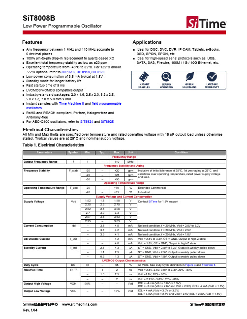
Electrical Characteristics
All Min and Max limits are specified over temperature and rated operating voltage with 15 pF output load unless otherwise stated. Typical values are at 25°C and nominal supply voltage.
+50 ppm Operating Temperature Range +70 °C
Hale Waihona Puke – +85 °C Industrial Supply Voltage and Current Consumption 1.8 2.5 2.8 3.0 3.3 – 3.8 3.7 3.5 – – 2.1 1.1 1.98 2.75 3.08 3.3 3.63 3.63 4.5 4.2 4.1 4.2 4.0 4.3 2.5 V V V V V V mA mA mA mA mA A A Contact SiTime for 1.5V support
Table 2. Pin Description
Pin Symbol Output Enable 1 OE/ST/NC Standby No Connect 2 3 4 GND OUT VDD Power Output Power Functionality H[1]: specified frequency output L: output is high impedance. Only output driver is disabled. H[1]: specified frequency output L: output is low (weak pull down). Device goes to sleep mode. Supply current reduces to I_std. Any voltage between 0 and Vdd or Open[1]: Specified frequency output. Pin 1 has no function. Electrical ground Oscillator output Power supply voltage[2] OE/ST/NC
32.768KHZ表晶技术参数图
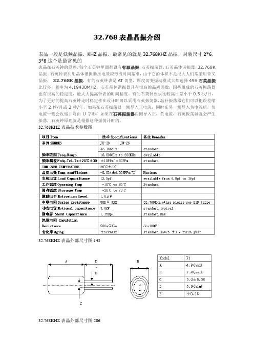
32.768表晶晶振介绍
表晶一般是低频晶振,KHZ晶振,最常见的就是32.768KHZ晶振,封装尺寸2*6,3*8这个是最常见的
表晶在石英钟的原理,每个石英钟里面都设有有源晶振,石英振荡器,石英晶体谐振器,32.768K 晶振。
石英钟表利用晶体谐振器压电效应形成时间基准,由于它的体积不是很大人们常采用音叉晶振,32.768K晶振,有的石英钟表是AT切型,厚度切变振动模式大都选择49S石英晶振比较多,频率为4.19430MHZ。
石英晶体谐振器具有很高的品质因数,因些组成的石英振荡器也有很高的稳定度,能大大提高钟表的时间精度。
有的石英钟要求比较高日差小于0.5秒/日,为了更好的提高石英钟走时稳定性在设计时可以采用石英振荡器,温补振荡器它们可以把误差缩小至2秒/月或2秒/年,如果在石英振荡器一侧导入正电流,同时在另一侧导入负电流后,负电流一侧会收缩并弯曲U字形,如果在石英振荡器两侧导入正,负电流,石英振荡器就会产生振荡,石英钟原理就是根据这种振荡计时的。
32.768KHZ表晶技术参数图
32.768KHZ表晶外部尺寸图:145
32.768KHZ表晶外部尺寸图:206
32.768KHZ表晶久尺寸图308。
KDS大真空DSK321STD 32.768Khz温补晶振1XZA032768AD19

9
Solderability
10 Resistance to Soldering heat
∆f/f ≦±5.0ppm No visible damage.
Serial No. : 2015-0806
DATE : 2015/08/06
ITEM :
CRYSTAL OSCILLATOR
DSK321STD
-------- ------ ------ ------ ------ ------ ------ ------ ----- ------ ------ ------ ------ ------ -------------------------------------------
2
Vibration
∆f/f ≦±5.0ppm
3
Shock
∆f/f ≦±5.0ppm
4
PCB bend strength
∆f/f ≦±5.0ppm No visible damage. No leak damage.
5
Adherence nature
6 7 8
Package strength Gross leak Fine leak
Ref. to Nominal Frequency Vcc=+3.3V,Ta=-40~+85 C Vcc=+3.3V, No Load Interval of temperature compensation : 0.5s IO L =0.1mA IO H =-0.1mA 0.5xVcc level 20~ 80%Vcc 80~ 20%Vcc From Vcc reaches the Supply Voltage, until the output
Sitime产品选型手册中文2012
p p
p p
-
p p
-
压控振荡器 — VCXO
SiT3807 网络、电信、 医疗、ATE、 视频、xDSL、 及嵌入式系统 VCXO • 可选标准频率,最大程度降低 成本 • 超低相位抖动: 0.5 psrms • 最广牵引范围 • 1%牵引线性度 • 超低相位抖动: 0.5 psrms 1.5-45 (标准频点范围) 1-80 10, 25, 50 80-220 25, 50 25-200 (1%线性度) CMOS LVTTL 32 70 µA (待机) C, I 2.5x2.0 mm 3.2x2.5 mm 5.0x3.2 mm 7.0x5.0 mm
-
-
要求低EMI的计算机 设备应用 应用、服务器
SiT9002
SSXO
• 扩频设计: 中心展频或向下 展频
1-220
25, 50
-
LVPECL LVDS HCSL CML
48-75
C, I
5.0x3.2 mm 7.0x5.0 mm
p
p
-
p
差分压控振荡器 — VCXO
SiT3821 网络、电信、 医疗、ATE、 视频、xDSL、 嵌入式系统 SiT3822 VCXO • 最佳稳定度 • 1%牵引线性度 • 超低相位抖动: 0.5 psrms 220-625 1-220 10, 25, 50 25-1600 (1% 牵引线 性度) LVPECL LVDS 55-69 C, I 5.0x3.2 mm 7.0x5.0 mm
单端数控振荡器 — DCXO
网络及电信
SiT3907
DCXO
• 单引脚串口可编程 • 0.1% 牵引线性度动 • 超低相位抖动 0.5 psrms
爱普生 EPSON 表晶谐振器 MC-146 32.768000 kHz 规格参数、数据手册、规格书信息
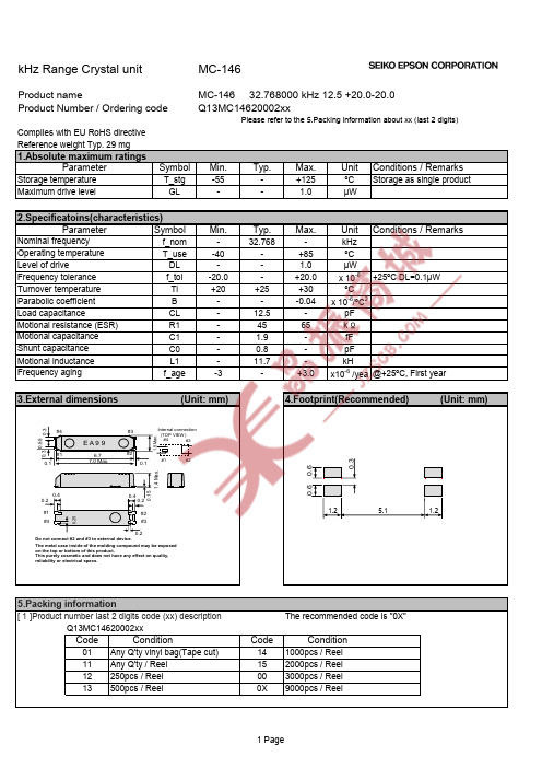
T_stg
-55
-
+125
ºC Storage as single product
Maximum drive level
GL
-
-
1.0
µW
2.Specificatoins(characteristics)
Parameter
Symbol
Nominal frequency
f_nom
Operating temperature
[ 2 ] Taping specification Subject to EIA-481 & IEC-60286
(1) Tape dimensions TE1604L Material of the Carrier Tape : PS Material of the Top Tape : PET+PE
+0.1
2.0±0.1
10P: 40±0.1 4.0±0.1
1.75±0.1
Unit: mm
0.3±0.05
1.7±0.1 (0.2)
7.2±0.1 (4.8 )
7.5±0.1 16.0±0.3
φ1.0
4.0±0.1
(2) Reel dimensions Material of the Reel : PS
1.7±0.1
Top Tape
Unit: mm
2 Page
Reflow profile
Pre Heating Temperature Tp1 ~ Tp2 = + 170 °C
Heating Temperature TMlt = + 220 °C
Peek Temperature TMax. = + 260 °C
32.768khz 温补晶振电路
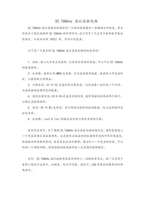
32.768khz 温补晶振电路
32.768kHz温补晶振电路通常由一个晶体振荡器和一些辅助元件组成,其目的是为了稳定地提供32.768kHz的时钟信号。
这个信号广泛应用于各种数字集成电路中,如实时时钟(RTC)等,作为计时基准。
以下是一个基本的32.768kHz温补晶振电路的组成部分:
1. 晶体:核心元件是石英晶体,它具有非常高的Q值,可以产生3
2.768kHz 的振荡频率。
2. 反相器:通常采用CMOS反相器,它为晶体提供偏置,使晶体工作在饱和区,以获得较大的增益。
3. 负载电容:C1和C2是晶体的负载电容,与反相器一起形成一个负阻,为晶体提供振荡所需的能量。
4. 温度补偿电容:C3和C4是温度补偿电容,通常连接到晶体的两个端子,以稳定其振荡频率。
5. 电阻:R1和R2是电阻,用于降低对晶体的驱动能量,防止晶体振坏或出现异常。
6. 反相器:inv2对invl的输出波形进行整形并驱动负载。
在实际应用中,为了确保32.768kHz温补晶振电路的稳定性,通常需要接上一个电容来稳定其振荡频率。
这是因为石英晶体的振荡频率受到外界环境温度、机械振动等因素的影响,容易发生波动和漂移。
通过加入一个适当的电容,可以形成一个谐振回路,使得晶振的振荡频率在一定范围内保持稳定。
此外,32.768kHz温补晶振电路具有体积小、功耗低等优点,被广泛应用于各种小型电子设备中,如腕表、电子计时器、温度计、LCD屏幕驱动器等的时钟电路中。
SiTime温补振荡器和三级钟产品培训
5023/4Diff
1-650 MHz 0.5 PPM
9121/2Diff
1-650 MHz
5301/2
1-220 MHz Stratum 3 Diff = Differential Output
7
400-888-2483
业界最为完整的全硅MEMS时钟产品系列
智能电网(Smart Grid)
LTE Access Points 网络同步定时协议 (1588)
14
测试设备
400-888-2483
不同类型(VC)TCXO的差异
标准频率和稳定度 市场均价 频率 $0.5 - $2.0 10-20 标准频率 (<40 MHz) 1 – 5 PPM WiFi, 3G VoIP Industrial tester 2.5x2.0 3.2x2.5 4-pin $0.7 - $5.0 10-20 标准频率 (<40 MHz) 0.5 PPM GPS Broadcast Video RFID 2.5x2.0 3.2x2.5 4-pin 定制频率和稳定度 $5 - $20 定制频率或 40MHz以上高频 0.1 - 0.5 PPM Broadband Router Switch 7.0x5.0 14.0x9.0 4, 6-pin 三级钟 $15 - $25 1-5 个标准频率 0.1 – 0.28 PPM 4.6 PPM (20-年) 0.37 PPM (24小时 holdover) Basestation Core routers Smart Grid 7.0x5.0 14.0x9.0 4, 6, 8, 10-pin
3
400-888-2483
2011 Encore产品推出计划
MC-306规格书 爱普生32.768kHz晶振
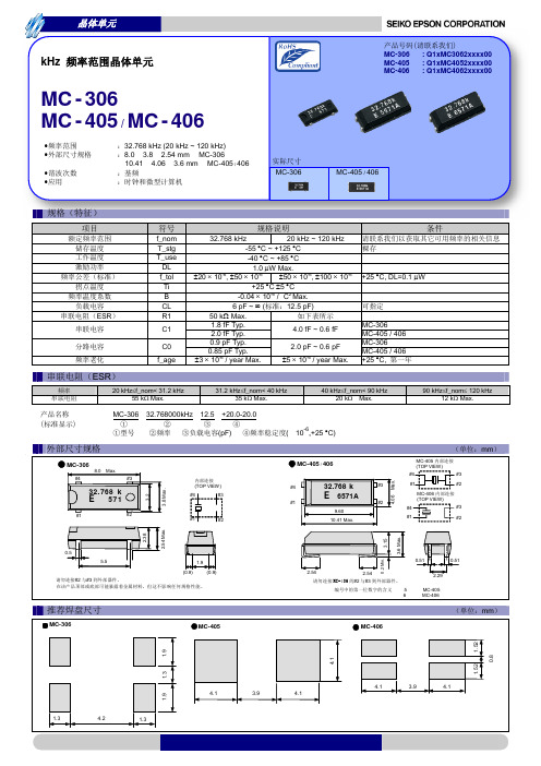
产品名称 (标准显示)
MC-306 ① ①型号
32.768000kHz 12.5 +20.0-20.0 ② ③ ④ -6 ②频率 ③负载电容(pF) ④频率稳定度(× 10 ,+25 C) (单位:mm)
MC-405 / 406
外部尺寸规格
.
MC-306
8.0 #4 Max. #3 内部连接 (TOP VIEW) #4 #3 #1
本材料中记载的品牌名称或产品名称是其所有人的商标或注册商标。
Seiko Epson Corporation
追求高品质
Seiko Epson 为了向顾客提供高品质、卓越信赖性的产品、服务,迅 速着手通过 ISO 9000 系列资格认证的工作,其日本和海外工厂也在通 过 ISO 9001 认证。 同时, 也在通过大型汽车制造厂商要求规格的 ISO/TS 16949 认证。 ISO/TS16949 是一项国际标准,是在 ISO9001 的基础上增 加了对汽车工业的特殊要求部分。
条件
请联系我们以获取其它可用频率的相关信息 裸存
+25 C, DL=0.1 W
可指定 MC-306 MC-405 / 406 MC-306 MC-405 / 406 +25 C, 第一年
串联电阻(ESR)
频率 串联电阻 20 kHzf_nom< 31.2 kHz 55 k Max. 31.2 kHzf_nom< 40 kHz 35 k Max. 40 kHzf_nom< 90 kHz 20 k Max. 90 kHzf_nom 120 kHz 12 k Max.
规格(特征)
项目
额定频率范围 储存温度 工作温度 激励功率 频率公差(标准) 拐点温度 频率温度系数 负载电容 串联电阻(ESR) 串联电容 分路电容 频率老化
- 1、下载文档前请自行甄别文档内容的完整性,平台不提供额外的编辑、内容补充、找答案等附加服务。
- 2、"仅部分预览"的文档,不可在线预览部分如存在完整性等问题,可反馈申请退款(可完整预览的文档不适用该条件!)。
- 3、如文档侵犯您的权益,请联系客服反馈,我们会尽快为您处理(人工客服工作时间:9:00-18:30)。
Jitter Performance (TA = over temp) Long Term Jitter Period Jitter 35 2.5 µspp nsRMS 81920 cycles (2.5 sec), 100 samples Cycles = 10,000, TA = 25°C, Vdd = 1.5V – 3.63V
32.768 kHz ±5, ±10, ±20 ppm frequency stability options over temp World’s smallest TCXO in a 1.5 x 0.8 mm CSP Operating temperature ranges: 0°C to +70°C -40°C to +85°C Ultra-low power: <1 µA Vdd supply range: 1.5V to 3.63V Improved stability reduces system power with fewer network timekeeping updates Internal filtering eliminates external Vdd bypass cap and saves space Pb-free, RoHS and REACH compliant
SiTime硅晶振样品中心 Rev. 1. 4
SiTime中国区技术支持
SiT1552
Smallest (1.2 mm ), Ultra-Low Power, 32.768 kHz MEMS TCXO
2
Table 1. Electrical Characteristics (continued)
Smart Meters (AMR) Health and Wellness Monitors Pulse-per-Second (pps) Timekeeping RTC Reference Clock
Electrical Specifications
Table 1. Electrical Characteristics
NanoDrive™ Programmable, Reduced Swing Output Output Rise/Fall Time Output Clock Duty Cycle AC-coupled Programmable Output Swing DC-Biased Programmable Output Voltage High Range DC-Biased Programmable Output Voltage Low Range Programmable Output Voltage Swing Tolerance tf, tf DC 48 0.20 to 0.80 0.60 to 1.225 0.35 to 0.80 -0.055 0.055 200 52 ns % SiT1552 does not internally AC-couple. This output description is intended for a receiver that is AC-coupled. See Table 4 for acceptable NanoDrive swing options. Vdd: 1.5V – 3.63V, 10 pF Load, IOH / IOL = ±0.2 μA. Vdd: 1.5V – 3.63V. IOH = -0.2 μA, 10 pF Load. See Table 4 for acceptable VOH/VOL setting levels. Vdd: 1.5V – 3.63V. IOL = 0.2 μA, 10 pF Load. See Table 4 for acceptable VOH/VOL setting levels. TA = -40°C to +85°C, Vdd = 1.5V to 3.63V. 30-70% (VOL/VOH), 10 pF Load
SiT1552
Smallest (1.2 mm2), Ultra-Low Power, 32.768 kHz MEMS TCXO Smallest (1.2mm2), Ultra-Low Power, 32.768 kHz MEMS TCXO Feห้องสมุดไป่ตู้tures
Applications
V_sw
V
VOH VOL
V V V
Table 2. Pin Configuration
CSP Pin 1, 4 Symbol GND I/O Power Supply Ground Functionality Connect to ground. All GND pins must be connected to power supply ground. The GND pins can be connected together, as long as both GND pins are connected ground. Oscillator clock output. When interfacing to an MCU’s XTAL, the CLK Out is typically connected to the receiving IC’s X IN pin. The SIT1552 oscillator output includes an internal driver. As a result, the output swing and operation is not dependent on capacitive loading. This makes the output much more flexible, layout independent, and robust under changing environmental and manufacturing conditions. Connect to power supply 1.5V ≤ Vdd ≤ 3.63V. Under normal operating conditions, Vdd does not require external bypass/decoupling capacitor(s). 3 Vdd Power Supply For more information about the internal power-supply filtering, see Power-Supply Noise Immunity section in the detailed description. Contact SiTime for applications that require a wider operating supply voltage range.
Notes: 1. No board level underfill. Measured as peak-to-peak/2. Inclusive of 3x-reflow and ±20% load variation. Tested with Agilent 53132A frequency counter. Due to the low operating frequency, the gate time must be ≥100 ms to ensure an accurate frequency measurement. 2. Initial offset is defined as the frequency deviation from the ideal 32.768 kHz at room temperature, post reflow. 3. Core operating current does not include output driver operating current or load current. To derive total operating current (no load), add core operating current + output driver operating current, which is a function of the output voltage swing. See the description titled Calculating Load Current.
Supply Voltage and Current Consumption Operating Supply Voltage Core Supply Current [3] Power-Supply Ramp Vdd Idd t_Vdd_ Ramp 180 Start-up Time at Power-up t_start 1.5 0.99 1.52 100 300 350 380 ms ms 3.63 V μA TA = -40°C to +85°C TA = 25°C, Vdd = 1.8V, LVCMOS Output configuration, No Load TA = -40°C to +85°C, Vdd = 1.5V – 3.63V, No Load Vdd Ramp-Up 0 to 90% Vdd, TA = -40°C to +85°C TA = -40°C +60°C, valid output TA = +60°C to +70°C, valid output TA = +70°C to +85°C, valid output