电通品牌蜂窝模式080512
NB-IOT之窄带蜂窝物联网解决方案

高安全性:NB-IoT采用加密技术,保障数据安全
04
应用场景
智能抄表:实现远程抄表,提高抄表效率
智能停车:实时监控车位状态,提高停车效率
智能路灯:实现远程控制,降低能耗
智能安防:实时监控,提高安全保障
智能物流:实时追踪货物,提高物流效率
智能农业:实时监测环境,提高农业生产效率
NB-IOT解决方案
03
5G技术的发展将推动NB-IOT在更多领域的应用
04
随着NB-IOT技术的不断成熟,市场前景将更加广阔
挑战与机遇
合作:与产业链上下游企业合作,共同推动NB-IOT的发展
04
竞争:与其他物联网技术的竞争,如LoRa、Sigfox等
03
机遇:物联网市场的快速增长、5G技术的发展、智慧城市建设等
02
挑战:技术成熟度、成本、功耗、覆盖范围等
谢谢
03
边缘计算:NB-IoT将与边缘计算技术结合,实现数据的实时处理和分析,提高物联网应用的智能化水平。
04
安全与隐私保护:NB-IoT将加强安全与隐私保护技术,确保物联网应用的安全性和可靠性。
市场前景
01
物联网市场规模不断扩大,NB-IOT将发挥重要作用
02
低功耗、广覆盖、低成本等特点使NB-IOT在众多应用场景中具有优势
NB-IOT的未来发展
点击此处添加正文,文字是您思想的提炼,为了演示发布的良好效果,请言简意赅的阐述您的观点。
4
技术趋势
01
低功耗广域网(LPWAN)技术:NB-IoT将广泛应用于物联网领域,满足低功耗、广覆盖、大连接的需求。
02
5G技术:NB-IoT将与5G技术融合,提供更高速、更低时延的连接,满足更多应用场景的需求。
TEC控制芯片85208521
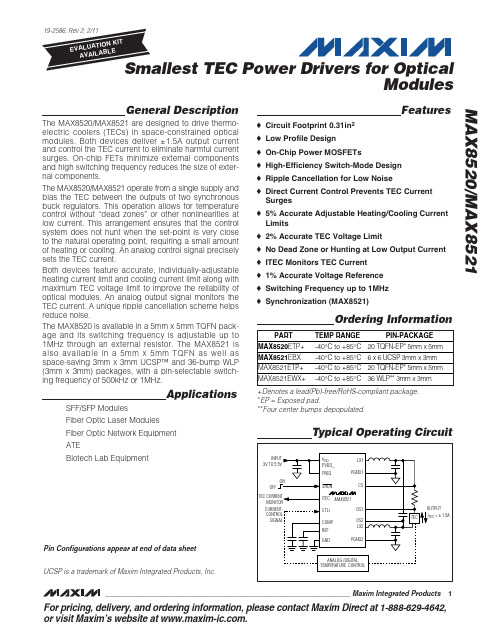
General DescriptionThe MAX8520/MAX8521 are designed to drive thermo-electric coolers (TE Cs) in space-constrained optical modules. Both devices deliver ±1.5A output current and control the TEC current to eliminate harmful current surges. On-chip FE Ts minimize external components and high switching frequency reduces the size of exter-nal components.The MAX8520/MAX8521 operate from a single supply and bias the TEC between the outputs of two synchronous buck regulators. This operation allows for temperature control without “dead zones” or other nonlinearities at low current. This arrangement ensures that the control system does not hunt when the set-point is very close to the natural operating point, requiring a small amount of heating or cooling. An analog control signal precisely sets the TEC current.Both devices feature accurate, individually-adjustable heating current limit and cooling current limit along with maximum TEC voltage limit to improve the reliability of optical modules. An analog output signal monitors the TEC current. A unique ripple cancellation scheme helps reduce noise.The MAX8520 is available in a 5mm x 5mm TQFN pack-age and its switching frequency is adjustable up to 1MHz through an external resistor. The MAX8521 is also available in a 5mm x 5mm TQFN as well as space-saving 3mm x 3mm UCSP™ and 36-bump WLP (3mm x 3mm) packages, with a pin-selectable switch-ing frequency of 500kHz or 1MHz.ApplicationsSFF/SFP Modules Fiber Optic Laser Modules Fiber Optic Network Equipment ATEBiotech Lab EquipmentFeatureso Circuit Footprint 0.31in 2o Low Profile Design o On-Chip Power MOSFETso High-Efficiency Switch-Mode Design o Ripple Cancellation for Low Noiseo Direct Current Control Prevents TEC Current Surges o 5% Accurate Adjustable Heating/Cooling Current Limits o 2% Accurate TEC Voltage Limito No Dead Zone or Hunting at Low Output Current o ITEC Monitors TEC Current o 1% Accurate Voltage Reference o Switching Frequency up to 1MHz o Synchronization (MAX8521)MAX8520/MAX8521Modules________________________________________________________________Maxim Integrated Products 1Ordering InformationFor pricing, delivery, and ordering information,please contact Maxim Direct at 1-888-629-4642,or visit Maxim’s website at .UCSP is a trademark of Maxim Integrated Products, Inc.Typical Operating CircuitPin Configurations appear at end of data sheet +Denotes a lead(Pb)-free/RoHS-compliant package.*EP = Exposed pad.**Four center bumps depopulated.M A X 8520/M A X 8521Smallest TEC Power Drivers for Optical ModulesABSOLUTE MAXIMUM RATINGSStresses beyond those listed under “Absolute Maximum Ratings” may cause permanent damage to the device. These are stress ratings only, and functional operation of the device at these or any other conditions beyond those indicated in the operational sections of the specifications is not implied. Exposure to absolute maximum rating conditions for extended periods may affect device reliability.V DD to GND..............................................................-0.3V to +6V SHDN , MAXV, MAXIP, MAXIN,CTLI to GND.........................................................-0.3V to +6V COMP, FREQ, OS1, OS2, CS, REF,ITEC to GND...........................................-0.3V to (V DD + 0.3V)PVDD1, PVDD2 to GND.............................-0.3V to (V DD + 0.3V)PVDD1, PVDD2 to V DD ..........................................-0.3V to +0.3V PGND1, PGND2 to GND.......................................-0.3V to +0.3V COMP, REF, ITEC short to GND....................................Indefinite LX Current (Note 1)........................................±2.25A LX Current Continuous Power Dissipation (T A = +70°C)6 x 6 UCSP (derate 22mW/°C above +70°C)...............1.75W 20-Pin 5mm x 5mm x 0.9mm TQFN (derate 20.8mW/°Cabove +70°C) (Note 2)...................................................1.67W 36-Bump WLP (derate 22mW/°C above +70°C)............1.75W Operating Temperature Range ...........................-40°C to +85°C Maximum Junction Temperature.....................................+150°C Storage Temperature Range.............................-65°C to +150°C Lead Temperature (soldering, 10s).................................+300°C Soldering Temperature (reflow)Lead(Pb)-Free (TQFN, WLP)........................................+260°C Containing Lead (UCSP).............................................+240°CELECTRICAL CHARACTERISTICSNote 1:LX has internal clamp diodes to PGND and PVDD. Applications that forward bias these diodes should take care not toexceed the IC’s package power dissipation limits.Note 2:Solders underside metal slug to PCB ground plane.PACKAGE THERMAL CHARACTERISTICS (Note 3)20 TQFNJunction-to-Ambient Thermal Resistance (θJA )...............30°C/W Junction-to-Case Thermal Resistance (θJC )......................2°C/W 6x6 UCSPJunction-to-Ambient Thermal Resistance (θJA )................65.5°C/W Junction-to-Case Thermal Resistance (θJC ).......................0°C/W36 WLPJunction-to-Ambient Thermal Resistance (θJA )..................38°C/W Junction-to-Case Thermal Resistance (θJC )......................4°C/WNote 3:Package thermal resistances were obtained using the method described in JEDEC specification JESD51-7, using a four-layer board. For detailed information on package thermal considerations, refer to /thermal-tutorial .MAX8520/MAX8521Smallest TEC Power Drivers for OpticalModules_______________________________________________________________________________________3ELECTRICAL CHARACTERISTICS (continued)M A X 8520/M A X 8521Smallest TEC Power Drivers for Optical Modules 4_______________________________________________________________________________________ELECTRICAL CHARACTERISTICS(V DD = V PVDD1= V PVDD2= V SHDN = 5V, 1MHz mode (Note 4). PGND1 = PGND2 = GND, CTLI = MAXV = MAXIP = MAXIN = REF, T A = -40°C to +85°C , unless otherwise noted.) (Note 8)MAX8520/MAX8521Smallest TEC Power Drivers for OpticalModules_______________________________________________________________________________________5ELECTRICAL CHARACTERISTICS (continued)(V= V = V = V = 5V, 1MHz mode (Note 4). PGND1 = PGND2 = GND, CTLI = MAXV = MAXIP = MAXIN = REF,the MAX8521.Note 5:Includes power FET leakage.Note 6:Duty-cycle specification is guaranteed by design and not production tested.Note 7:CTLI Gain is defined as:Note 8:Specifications to -40°C are guaranteed by design and not production tested.Typical Operating Characteristics(V DD = 5V, circuit of Figure 1, T A = +25°C unless otherwise noted.)EFFICIENCY vs. TEC CURRENTV DD = 5V, R TEC = 2ΩTEC CURENT (A)E F F I C I E N C Y (%)1.41.20.810.40.60.2102030405060708090001.6EFFICIENCY vs. TEC CURRENT V DD = 3.3V, R TEC = 1.3ΩTEC CURRENT (A)E F F I C I E N C Y (%)1.41.20.810.40.60.21020304050607080901.6COMMON-MODE OUTPUT VOLTAGE RIPPLEMAX8520/21 toc03400ns/divV OS220mV/div AC-COUPLEDV OS120mV/div AC-COUPLED I TEC = 1AC 2 = C 7 = 1µFM A X 8520/M A X 8521Smallest TEC Power Drivers for Optical Modules 6_______________________________________________________________________________________DIFFERENTIALOUTPUT VOLTAGE RIPPLEMAX8520/21 toc04400ns/divV OS2 - V OS11mV/divAC-COUPLEDC 2 = C 7 = 1µFI TEC = 1AV DD RIPPLEMAX8520/21 toc05400ns/div V DD20mV/div AC-COUPLEDI TEC = 1ATEC CURRENT RIPPLEMAX8520/21 toc06400ns/div10mA/div AC-COUPLED0A1.5ATEC CURRENT vs. CTLI VOLTAGEMAX8520/21 toc0720ms/divV CTLI 1V/divI TEC1A/div0A 0VZERO-CROSSING TEC CURRENTMAX8520/21 toc081ms/divV CTLII00mV/divI TEC100mA/div0A 1.5VV ITEC vs. TEC CURRENTTEC CURRENT (A)V I T E C (V )1.51.00.5-0.5-1.0-1.50.51.01.52.02.53.0-2.02.0Typical Operating Characteristics (continued)(V DD = 5V, circuit of Figure 1, T A = +25°C unless otherwise noted.)I TEC vs. AMBIENT TEMPERATUREAMBIENT TEMPERATURE (°C)T E C C U R R E N T (A )+60+40+20-200.4600.4700.4800.4900.5000.5100.5200.450-40+80SWITCHING FREQUENCY vs. TEMPERATURETEMPERATURE (°C)S W I T C H I N G F R E Q U E N C Y (k H z )+80+60+40+200-2050060070080090010001100400-40MAX8520/MAX8521Smallest TEC Power Drivers for OpticalModules_______________________________________________________________________________________7SWITCHING FREQUENCY CHANGE vs. V DDV DD (V)S W I T C H I N G F R E Q U E N C Y C H A N G E (k H z )5.04.54.03.52004006008001000120003.05.5SWITCHING FREQUENCY vs. R EXTR EXT (k Ω)S W I T C H I N G F R E Q U E N C Y (k H z )140120100805006007008009001000110040060160V DD STEP RESPONSEMAX8520/21 toc1910ms/divV DD 2V/divI TEC10mA/div1A0VREFERENCE VOLTAGE CHANGE vs. V DDV DD (V)R E F E R E N C E V O L T A G E C H A N G E (m V )5.04.54.03.5-1.2-1.0-0.8-0.6-0.4-0.200.20.40.6-1.43.0 5.5REFERENCE VOLTAGE CHANGEvs. TEMPERATURETEMPERATURE (°C)R E F E R E N C E V O L T A G E C H A N G E (m V )+80+40+60+20-20-4-3-2-1012345-5-40REFERENCE VOLTAGE CHANGEvs. LOAD CURRENTLOAD CURRENT (mA)R E F E R E N C E V O L T A G E C H A N G E (m V )0.80.60.40.2-10-8-6-4-20-121.0STARTUP AND SHUTDOWN WAVEFORMSMAX8520/21 toc17200µs/divV SHDN 5V/div I TEC500mA/div I DD200mA/div 0mA0mA0V CTLI STEP RESPONSEMAX8520/21 toc181msV CTLI 1V/div I TEC 1A/div0A 1.5VTypical Operating Characteristics (continued)(V DD = 5V, circuit of Figure 1, T A = +25°C unless otherwise noted.)M A X 8520/M A X 8521Smallest TEC Power Drivers for Optical Modules 8_______________________________________________________________________________________Typical Operating Characteristics (continued)(V DD = 5V, circuit of Figure 1, T A = +25°C unless otherwise noted.)THERMAL STABILITY,COOLING MODEMAX8520/21 toc204s/divTEMPERATURE 0.001°C/div T TEC = +25°C T A = +45°CTHERMAL STABILITY,ROOM TEMPERATUREMAX8520/21 toc214s/divTEMPERATURE 0.001°C/div T TEC = +25°C T A = +25°CTHERMAL STABILITY,HEATING MODEMAX8520/21 toc224s/divTEMPERATURE 0.001°C/divT TEC = +25°C T A = +5°CPin DescriptionMAX8520/MAX8521Smallest TEC Power Drivers for OpticalModules_______________________________________________________________________________________9Pin Description (continued)M A X 8520/M A X 8521Smallest TEC Power Drivers for Optical Modules 10______________________________________________________________________________________Detailed DescriptionThe MAX8520/MAX8521 TE C drivers consist of two switching buck regulators that operate together to directly control the TEC current. This configuration cre-ates a differential voltage across the TE C, allowing bi-directional TE C current for controlled cooling and heating. Controlled cooling and heating allow accurate TEC temperature control to within 0.01°C. The voltage at CTLI directly sets the TEC current. An external thermal-control loop is typically used to drive CTLI. Figures 1and 2 show examples of the thermal-control-loop circuit.Ripple CancellationSwitching regulators like those used in the MAX8520/MAX8521 inherently create ripple voltage on the output.The dual regulators in the MAX8520/MAX8521 switch in-phase and provide complementary in-phase duty cycles so ripple waveforms at the TE C are greatly reduced. This feature suppresses ripple currents and electrical noise at the TEC to prevent interference with the laser diode.Switching FrequencyFor the MAX8521, FRE Q sets the switching frequency of the internal oscillator. With FREQ = GND, the oscilla-tor frequency is set to 500kHz. The oscillator frequency is 1MHz when FREQ = V DD .For the MAX8520, connect a resistor (R EXT in Figure 2)from FRE Q to GND. Choose R EXT = 60k Ωfor 1MHz operation, and R EXT = 150k Ωfor 500KHz operation. For any intermediary frequency between 500kHz and 1MHz, use the following equation to find the value of R EXT value needed for V DD = 5V:where R EXT is the resistance given in k Ω, and fs is the desired frequency given in MHz. Note that for V DD <5V, the frequency is reduced slightly, to the extent of about 7% when V DD reaches 3V. This should be taken into consideration when selecting the value for R EXT at known supply voltage.Voltage and Current-Limit SettingBoth the MAX8520 and MAX8521 provide control of the maximum differential TE C voltage. Applying a voltage to MAXV limits the maximum voltage across the TE C.The voltage at MAXIP and MAXIN sets the maximum positive and negative current through the TE C. These current limits can be independently controlled.Current Monitor OutputITEC provides a voltage output proportional to the TEC current (I TEC ). See the Functional Diagram for more detail:V ITEC = 1.5V +(8 (VOS1-VCS))Reference OutputThe MAX8520/MAX8521 include an on-chip voltage ref-erence. The 1.50V reference is accurate to 1% over temperature. Bypass REF with 0.1µF to GND. REF can be used to bias an external thermistor for temperature sensing as shown in Figures 1 and 2.Thermal and Fault-Current ProtectionThe MAX8520/MAX8521 provide fault-current protec-tion in either FE Ts by turning off both high-side and low-side FE Ts when the peak current exceeds 3A in either FE Ts. In addition, thermal-overload protection limits the total power dissipation in the chip. When the device’s die junction temperature exceeds +165°C, an on-chip thermal sensor shuts down the device. The thermal sensor turns the device on again after the junc-tion temperature cools down by +15°C.Design ProceduresDuty-Cycle Range SelectionBy design, the MAX8520/MAX8521 are capable of operating from 0% to 100% duty cycle, allowing both LX outputs to enter dropout. However, as the LX pulse width narrows, accurate duty-cycle control becomes difficult. This can result in a low-frequency noise appearing at the TEC output (typically in the 20kHz to 50kHz range). While this noise is typically filtered out by the low thermal-loop bandwidth, for best result, operate the PWM with a pulse width greater than 200ns. For 500kHz application, the recommended duty-cycle range is from 10% to 90%. For 1MHz application, it is from 20% to 80%.MAX8520/MAX8521Smallest TEC Power Drivers for OpticalModules______________________________________________________________________________________11Figure 1. MAX8521 Typical Application CircuitM A X 8520/M A X 8521Smallest TEC Power Drivers for Optical Modules 12______________________________________________________________________________________Figure 2. Typical Application Circuit for the MAX8520 with Reduced Op-Amp Count ConfigurationMAX8520/MAX8521Smallest TEC Power Drivers for OpticalModules______________________________________________________________________________________13Inductor SelectionThe MAX8520/MAX8521 dual buck converters operate in-phase and in complementary mode to drive the TEC differentially in a current-mode control scheme. At zero TEC current, the differential voltage is zero, hence the outputs with respect to GND are equal to half of V DD .As the TEC current demand increases, one output will go up and the other will go down from the initial point of 0.5V DD by an amount equal to 0.5 V TEC (V TEC = I TEC R TEC ). Therefore, the operating duty cycle of each buck converter depends on the operating I TEC and R TEC . Since inductor current calculation for heating and cooling are identical, but reverse in polarity, the calcu-lation only needs to be carried out for either one.For a given inductor, and input voltage, the maximum inductor ripple current happens when the duty cycle is at 50%. Therefore, the inductor should be calculated at 50% duty cycle to find the maximum ripple current. The maximum desired ripple current of a typical standard buck converter is in the range of 20% to 40% of the maximum load. The higher the value of the inductor, the lower the ripple current. However, the size will be phys-ically larger. For the TE C driver the thermal loop is inherently slow, so the inductor can be larger for lower ripple current for better noise and E MI performance.Picking an inductor to yield ripple current of 10% to 20% of the maximum TE C current is a good starting point.Calculate the inductor value as follows:where LIR is the selected inductor ripple-current ratio,I TEC(MAX)is the maximum TE C current, and fs is the switching frequencyAs an example, for V DD = 3.3V, LIR = 12%, and fs =1MHz, L = 4.58µHEven though each inductor ripple current is at its maxi-mum at 50% duty cycle (zero TE C current), the ripple cancels differentially because each is equal and in-phase.Output Filter Capacitor SelectionCommon-Mode Filter CapacitorsThe common-mode filter capacitors (C2 and C7 of Figure 1) are used as filter capacitors to ground for each output. The output ripple voltage depends on the capacitance, the E SR of these capacitors, and the inductor ripple current. Ceramic capacitors are recom-mended for their low E SR and impedance at high fre-quency.Figure 3. Functional Diagram of the Current-Control LoopM A X 8520/M A X 8521The output common-mode ripple voltage can be calcu-lated as follows:V RIPPLEpk-pk = LIR x I TEC(MAX)(ESR + 1/8 x C x fs)A 1µF ceramic capacitor with ESR of 10 m Ωwith LIR =12% and I TEC(MAX)= 1.5A will result in V RIPPLE(P-P)of 24.3mV. For size-constraint application, the capacitor can be made smaller at the expense of higher ripple voltage. However, the capacitance must be high enough so that the LC resonant frequency is less than 1/5 the switching frequency:where f is the resonant frequency of the output filter.Differential Mode Filter CapacitorThe differential-mode filter capacitor (C5 in Figure 1) is used to bypass differential ripple current through the TEC as the result of unequal duty cycle of each output.This happens when the TE C current is not at zero. As TE C current increases from zero, both outputs move away from the 50% duty-cycle point complementarily.The common-mode ripple decreases, but the differential ripple does not cancel perfectly, and there will be a resulting differential ripple. The maximum value happens when one output is at 75% duty cycle and the other is at 25% duty cycle. At this operating point, the differential ripple is equal to 1/2 of the maximum common-mode rip-ple. The TE C ripple current determines the TE C perfor-mance, because the maximum temperature differential that can be created between the terminals of the TE C depends on the ratio of ripple current and DC current.The lower the ripple current, the closer to the ideal maxi-mum. The differential-mode capacitor provides a low-impedance path for the ripple current to flow, so that the TE C ripple current is greatly reduced. The TE C ripple current then can be calculated as follows:I TEC(RIPPLE)= (0.5 x LIR x I TEC(MAX)) x (Z C5)/(R TEC+ R SENSE + Z C5)where Z C5is the impedance of C5 at twice the switching frequency, R TEC is the TE C equivalent resistance, and R SENSE is the current-sense resistor.Decoupling Capacitor SelectionDecouple each power supply input (V DD , PVDD1,PVDD2) with a 1µF ceramic capacitor close to the sup-ply pins. In applications with long distances between the source supply and the MAX8520/MAX8521, addi-tional bypassing may be needed to stabilize the input supply. In such cases, a low-ESR electrolytic or ceramic capacitor of 100µF or more at V DD is sufficient.Compensation CapacitorA compensation capacitor is needed to ensure current-control-loop stability (see Figure 3). Select the capacitor so that the unity-gain bandwidth of the current-control loop is less than or equal to 10% the resonant frequency of the output filter:where:f BW = Unity-gain bandwidth frequency, less than or equal to 10% the output filter resonant frequencyg m = Loop transconductance, typically 100µA/V C COMP = Value of the compensation capacitorR TEC = TEC series resistance, use the minimum resis-tance valueR SENSE = Sense resistorSetting Voltage and Current LimitsCertain TEC parameters must be considered to guarantee a robust design. These include maximum positive current,maximum negative current, and the maximum voltage allowed across the TEC. These limits should be used to set the MAXIP, MAXIN, and MAXV voltages.Setting Max Positive and Negative TEC Current MAXIP and MAXIN set the maximum positive and nega-tive TEC currents, respectively. The default current limit is ±150mV/R SENSE when MAXIP and MAXIN are con-nected to RE F. To set maximum limits other than the defaults, connect a resistor-divider from REF to GND to set V MAXI_. Use resistors in the 10k Ωto 100k Ωrange.V MAXI_is related to ITEC by the following equations:V MAXIP = 10(I TECP(MAX) R SENSE )V MAXIN = 10(I TECN(MAX) R SENSE )where I TECP(MAX)is the maximum positive TEC current and I TECN(MAX)is the negative maximum TEC current.Positive TEC current occurs when CS is less than OS1:I TEC x R SENSE = OS1 - CSwhen I TEC > 0A.I TEC R SENSE = CS - OS1when I TEC< 0A.Smallest TEC Power Drivers for Optical Modules 14______________________________________________________________________________________Take care not to exceed the positive or negative cur-rent limit on the TEC. Refer to the manufacturer’s data sheet for these limits.Setting Max TEC Voltage Apply a voltage to the MAXV pin to control the maxi-mum differential TEC voltage. V MAXV can vary from 0V to V REF. The voltage across the TE C is four times V MAXV and can be positive or negative:|V OS1- V OS2| = 4 x V MAXV or V DD, whichever is lower Set V MAXV with a resistor-divider between RE F and GND using resistors from 10kΩto 100kΩ. V MAXV can vary from 0V to V REF.Control Inputs/OutputsOutput Current Control The voltage at CTLI directly sets the TEC current. CTLI is typically driven from the output of a temperature con-trol loop. The transfer function relating current through the TEC (I TEC) and V CTLI is given by:I TEC= (V CTLI- V REF)/(10 R SENSE)where V REF is 1.50V and:ITEC = (V OS1- V CS)/R SENSECTLI is centered around REF (1.50V). I TEC is zero when CTLI = 1.50V. When V CTLI> 1.50V the current flow is from OS2 to OS1. The voltages on the pins relate as follows:V OS2> V OS1> V CSThe opposite applies when V CTLI< 1.50V current flows from OS1 to OS2:V OS2< V OS1< V CSShutdown Control The MAX8520/MAX8521 can be placed in a power-saving shutdown mode by driving SHDN low. When the MAX8520/MAX8521 are shut down, the TEC is off (OS1 and OS2 decay to GND) and supply current is reduced to 2mA (typ).ITEC Output ITEC is a status output that provides a voltage proportional to the actual TEC current. V ITEC= V REF when TEC current is zero. The transfer function for the ITEC output is:V ITEC= 1.50V + 8 (V OS1– V CS)Use ITE C to monitor the cooling or heating current through the TE C. For stability keep the load capaci-tance on ITEC to less than 150pF.Applications InformationThe MAX8520/MAX8521 typically drive a thermo-elec-tric cooler inside a thermal-control loop. TE C drive polarity and power are regulated based on temperature information read from a thermistor or other temperature-measuring device to maintain a stable control tempera-ture. Temperature stability of +0.01°C can be achievedwith carefully selected external components.There are numerous ways to implement the thermal loop. Figures 1 and 2 show designs that employ precision op amps, along with a DAC or potentiometer to set the con-trol temperature. The loop can also be implemented digi-tally, using a precision A/D to read the thermistor or other temperature sensor, a microcontroller to implement the control algorithm, and a DAC (or filtered-PWM signal) tosend the appropriate signal to the MAX8520/MAX8521CTLI input. Regardless of the form taken by the thermal-control circuitry, all designs are similar in that they read temperature, compare it to a set-point signal, and thensend an error-correcting signal to the MAX8520/MAX8521 that moves the temperature in the appropriate direction.PCB Layout and RoutingHigh switching frequencies and large peak currentsmake PCB layout a very important part of design. Good design minimizes excessive EMI and voltage gradientsin the ground plane, both of which can result in instabil-ity or regulation errors. Follow these guidelines for goodPCB layout:1) Place decoupling capacitors as close to the IC pinsas possible.2) Keep a separate power ground plane, which is con-nected to PGND1 and PGND2. PVDD1, PVDD2, PGND1 and PGND2 are noisy points. Connect decou-pling capacitors from PVDD_ to PGND_ as direct as possible. Output capacitors C2, C7 returns are con-nected to PGND plane.3) Connect a decoupling capacitor from V DD to GND. Connect GND to a signal ground plane (separate fromthe power ground plane above). Other V DD decoupling capacitors (such as the input capacitor) need to be connected to the PGND plane.4) Connect GND and PGND_ pins together at a single point, as close as possible to the chip.5) Keep the power loop, which consists of input capaci-tors, output inductors and capacitors, as compact andsmall as possible.MAX8520/MAX8521Smallest TEC Power Drivers for OpticalModules ______________________________________________________________________________________15M A X 8520/M A X 85216) To ensure high DC-loop gain and minimum loop error, keep the board layout adjacent to the negative input pin of the integrator (U2 in Figure1) clean and free of moisture. Any contamination or leakage current into this node can act to lower the DC gain of the integrator which can degrade the accuracy of the thermal loop. If space is available, it can also be helpful to surround the negative input node of the integrator with a grounded guard ring.Refer to the MAX8520/MAX8521 evaluation kit for a PCB layout example.Chip InformationPROCESS: BiCMOSSmallest TEC Power Drivers for Optical Modules 16______________________________________________________________________________________F6PVDD2LX2LX2LX1LX1PGND2PGND2PGND2PGND1PGND1PGND1OS2FREQ GND2GND2COMP SHDN VDD GND2GND2ITECGNDCTLIREFMAXVMAX8521MAXIP MAXIN PVDD2CS OS1PVDD1PVDD1F5F4F3F2F1E6E5E2E1D6D5D4D3D2D1C6C5C4C3C2C1B6B5B2B1A6A5A4A3A2A1+UCSP/WLPTOP VIEW BUMPS ON BOTTOMPin ConfigurationsPackage InformationFor the latest package outline information and land patterns (footprints), go to /packages . Note that a “+”, “#”, or “-” in the package code indicates RoHS status only. Package drawings may show a different suffix character, but the drawing per-tains to the package regardless of RoHS status.MAX8520/MAX8521Smallest TEC Power Drivers for OpticalModules______________________________________________________________________________________17Functional Diagram。
导热绝缘灌封胶GMX-8152

h
电气强度
MV/m
18
18
18
介电常数,1MHz
5
5
5
硫 介电损耗,1MHz 化 体积电阻 后 Shore A 硬度
Ω.cm
0.01 1.0× 10¹³ 40±5
0.01 1.0× 10¹³ 60±5
0.01 1.0× 10¹³ 50~60
Shore 00 硬度
阻燃性
V-0
V-0
V-0
氧指数
%
37
导热系数
中蓝晨光化工研究院有限公司
蓝星(成都)新材料有限公司
包装 贮存 运输
注意事项
硅橡胶 RTV-2
GMX-8152 采用大口塑料桶分别包装,包装的 规格有 2×5Kg、2×10Kg、2×20Kg。 GMX-8152 贮存在 0℃~30℃之间,原包装密 闭条件下保质期为 6 个月以上。贮存期超过保 质期限并不意味着本产品完全不可用。在这种 情况下相关性能都应做质量检测以保其品质。 胶料按非危险品运输。
相容性
特定材料、化合物、硫化剂和增塑剂会阻碍 GMX-8152 的硫化。主要包括: y 有机锡和其它有机金属化合物 y 含有机锡催化剂的硅橡胶 y 硫、聚硫化物、聚砜类物或其它含硫物品 y 胺、氨基甲酸乙酯或含胺物品 y 不饱和的碳氢增塑剂 y 一些助焊剂残余物 如果对某一物体或材料是否会引起阻碍硫化 有疑问,建议作小型的相容性试验,以确定在 此应用中的适用性。如果在有疑问的物体和硫 化凝胶表面中存在液体或没有硫化的物质,表 明没有相容性,即会阻碍硫化。
中蓝晨光化工研究院有限公司 硅橡胶事业部
蓝星(成都)新材料有限公司
电话: 86-28-85583962, 85558462,85586001 网址:
SM7055-12_12V0.25A_BuckBoost
芯片概述
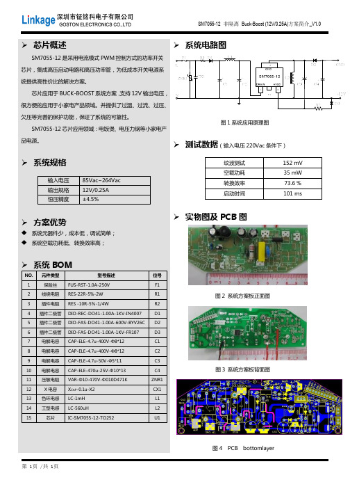
系统电路图
SM7055-12 是采用电流模式 PWM 控制方式的功率开关
芯片,集成高压启动电路和高压功率管,为低成本开关电源系
统提供高性价比的解决方案。
芯片应用于 BUCK-BOOST 系统方案,支持 12V 输出电压,
R1
3
插件电阻 RES -10R-5%DIO-REC-DO41-1.00A-1KV-IN4007
D1
5 插件二极管 DIO-FAS-DO41-1.00A-600V-BYV26C D2
6 插件二极管 DIO-FAS-DO41-1.00A-1KV-FR107
D3
7
电解电容 CAP-ELE-4.7u-400V-Ф8*12
很方便的应用于小家电产品领域。并提供了过温、过流、过压、
欠压等完善的保护功能,保证了系统的可靠性。 SM7055-12 芯片应用领域:电饭煲、电压力锅等小家电产
图 1 系统应用原理图
品电源。
测试数据(输入电压 220Vac 条件下)
系统规格
输入电压 输出规格 恒压精度
85Vac~264Vac 12V/0.25A ±4.5%
13 色环电感 LC-1mH
L1
14 工型电感 LC-560uH
L2
15
芯片
IC-SM7055-12-TO252
U1
图 2 系统方案板正面图 图 3 系统方案板背面图
第 1页 /共 1页
图 4 PCB bottomlayer
纹波测试 空载功耗 转换效率 启动时间
152 mV 35 mW 73.6 % 101 ms
莫莎公司 OnCell G2111 G2151I 系列工业四频GSM GPRS模块产品简介说明书

OnCell G2111/G2151I SeriesIndustrial quad-band GSM/GPRS modemsFeatures and Benefits•Quad-band GSM/GPRS850/900/1800/1900MHz•DIN-rail mounting and wall mounting•2.5kV RMS isolation for1min.for all serial signals(G2151I only)•LED indicators for GSM/GPRS and data transmission status•Extended operating temperature from-25to70°C(G2111-T only)CertificationsIntroductionThe OnCell G2111/G2151I Series of industrial quad-band GSM/GPRS modems are designed to transmit data and short messages(SMS)over GSM/ GPRS mobile networks.The modems can be used to increase the efficiency of maintenance and communication,but do not require extensive training.In addition,the modems can be mounted on a DIN rail or wall.The OnCell G2111/G2151I Series modems accept a12to48VDC power input,making them suitable for use with a variety of field power sources.The serial ports feature15kV ESD line protection to protect the products from harmful electrical discharge,and separate RS-232and RS-422/485 interfaces are built into the OnCell G2151I,each with2.5kV RMS isolation protection for one minute.The two serial interfaces on the OnCell G2151I make it ideal for attaching all kinds of devices,such as stand-alone controllers,PC COM ports,and multi-dropped electric meters.In addition,the OnCell G2111-T has an extended operating temperature(-25to70°C)design that makes it suitable for heavy industrial use. SpecificationsCellular InterfaceCellular Standards GSM,GPRSBand Options Quad-band GSM/GPRS850MHz/900MHz/1800MHz/1900MHzGPRS Multi-Slot Class10GPRS Terminal Device Class Class BGPRS Coding Schemes CS1to CS4CSD Data Rates Up to14400bpsCellular Antenna Connectors1SMA femaleNo.of SIMs1SIM Control Voltage3VSerial InterfaceNo.of Ports1Serial Standards All models:RS-232(DB9female connector)OnCell G2151I:RS-232/422/485(5-pin terminal block connector)ESD Protection OnCell G2111:15kVIsolation OnCell G2151I:2kVData Bits8Stop Bits1Parity NoneFlow Control RTS/CTSBaudrate300bps to230.4kbpsSerial SignalsRS-232TxD,RxD,RTS,CTS,DTR,DSR,DCD,RI,GNDRS-422Tx+,Tx-,Rx+,Rx-,GNDRS-485-2w Data+,Data-,GNDRS-485-4w Tx+,Tx-,Rx+,Rx-,GNDPower ParametersInput Voltage12to48VDCPower Connector Terminal blockInput Current0.625A@12VDC,0.16A@48VDCPhysical CharacteristicsHousing ABS+PolycarbonateIP Rating IP30Dimensions27x123x79mm(1.06x4.84x3.11in)Weight155g(0.34lb)Environmental LimitsOperating Temperature OnCell G2111/G2151I:-20to55°C(-4to131°F)OnCell G2111I-T:-25to70°C(-22to158°F)Storage Temperature(package included)-40to75°C(-40to167°F)Ambient Relative Humidity5to95%(non-condensing)Standards and CertificationsSafety UL60950-1EMC EN55032/24EMI CISPR32,FCC Part15B Class AEMS IEC61000-4-2ESD:Contact:4kV;Air:8kVIEC61000-4-3RS:80MHz to1GHz:3V/mIEC61000-4-4EFT:Power:0.5kVIEC61000-4-5Surge:Power:1kVIEC61000-4-6CS:3VIEC61000-4-8PFMFRadio Frequency FCC Part22H,FCC Part24E,EN301489-1,EN301489-7,EN301511MTBFTime OnCell G2111:925,000hrsOnCell G2111-T:925,000hrsOnCell G2151I:864,000hrsStandards Telcordia SR332WarrantyWarranty Period5yearsDetails See /warrantyPackage ContentsDevice1x OnCell G2111/G2151I Series GSM/GPRS modem1Antenna1x GSM/GPRSAccessory1x terminal block for power jack connectorDocumentation1x quick installation guide1x warranty cardDimensionsOrdering InformationModel Name Cellular Standard Band Operating Temp.Serial Isolation Serial StandardsOnCell G2111GSM/GPRS 850/900/1800/1900MHz-20to55°C–RS-232OnCell G2111-T GSM/GPRS 850/900/1800/1900MHz-25to70°C–RS-232OnCell G2151I GSM/GPRS 850/900/1800/1900MHz-20to55°C✓RS-232/422/4851.An activated SIM card(not included)must be provided by a third party Cellular Service Provider.Accessories(sold separately)AntennasANT-CQB-AHSM-00-3m GSM/GPRS/EDGE,omni-directional magnetic base antenna,0dBi,3m cableANT-CQB-AHSM-03-3m GSM/GPRS/EDGE,omni-directional magnetic base antenna,3dBi,3m cableANT-CQB-AHSM-05-3m GSM/GPRS/EDGE,omni-directional magnetic base antenna,5dBi,3m cableANT-CQB-ASM-01GSM/GPRS/EDGE,omni-directional rubber duck antenna,1dBiANT-WCDMA-ANF-00GSM/GPRS/EDGE/UMTS/HSPA,omni-directional outdoor antenna,0dBiANT-WCDMA-ASM-1.5GSM/GPRS/EDGE/UMTS/HSPA,omni-directional rubber duck antenna,1.5dBiANT-WCDMA-AHSM-04-2.5m GSM/GPRS/EDGE/UMTS/HSPA,omni-directional magnetic base antenna,4dBiANT-LTE-ASM-02GPRS/EDGE/UMTS/HSPA/LTE,omni-directional rubber duck antenna,2dBiANT-LTE-ANF-04GSM/GPRS/EDGE/UMTS/HSPA/LTE,omni-directional outdoor antenna,4dBi,IP66AntennasANT-LTEUS-ASM-01GSM/GPRS/EDGE/UMTS/HSPA/LTE,omni-directional rubber duck antenna,1dBiWireless Antenna CableA-CRF-SMSF-R3-100Cellular magnetic-base SMA connector with1-meter RF cable©Moxa Inc.All rights reserved.Updated Nov12,2018.This document and any portion thereof may not be reproduced or used in any manner whatsoever without the express written permission of Moxa Inc.Product specifications subject to change without notice.Visit our website for the most up-to-date product information.。
蜂巢电子产品指南:第十一月二〇二〇版本B,第二个标准产品提供说明书
Standard Product Offerings* Special order onlyOther products may be available. Refer to individual EW-series’ sheets for full range of solutionsNote: All images herein are generic and may not be representative of actual productElliptical Waveguide and AccessoriesProduct GuideEW17 Series (Special Order Only)Connectors Auxiliary ProductsAccessoriesEW20 Series (Special Order Only)Connectors Auxiliary ProductsAccessoriesEW28 Series (Special Order Only)Connectors Auxiliary ProductsAccessoriesHoistingEW37 SeriesConnectors Auxiliary ProductsAccessoriesEW43 SeriesConnectors Auxiliary ProductsAccessoriesEW52 SeriesConnectors Auxiliary ProductsAccessoriesEW63 SeriesConnectors Auxiliary ProductsAccessoriesHoistingEW64 SeriesConnectors Auxiliary ProductsAccessoriesEW77 SeriesConnectors Auxiliary ProductsAccessoriesEW85 SeriesConnectors Auxiliary ProductsAccessoriesEW90 SeriesConnectors Auxiliary ProductsAccessoriesHoistingEW127A SeriesConnectors Auxiliary ProductsAccessoriesEW132 SeriesConnectors Auxiliary ProductsAccessoriesHoistingEW180 SeriesConnectors Auxiliary ProductsAccessoriesHoistingEW220 SeriesConnectors Auxiliary ProductsAccessoriesHoistingEW240 SeriesConnectors Auxiliary ProductsAccessoriesConnector KitsSplice HardwareGrounding KitsUniversal Grounding Kit 60”UG1215B4-TCompatible with EW63 – EW180Individual specifications can be found in the E-CatalogWaveguide HangersWaveguide Entry EquipmentBoot AssembliesEntrance PanelsElliptical Waveguide - CommScope vs. CompetitorsVisit our website or contact your local CommScope representative for more information.© 2020 CommScope, Inc. All rights reserved.All trademarks identified by ® or ™ are registered trademarks or trademarks, respectively, of CommScope, Inc. This document is for planning purposes only and is not intended to modify or supplement any specifications or warrantie,d in accordance with international standards, including ISO 9001, TL 9000, and ISO 14001.Further information regarding CommScope’s commitment can be found at /About-Us/Corporate-Responsibility-and-Sustainability .CO-114132.1-EN (12/20)CommScope pushes the boundaries ofcommunications technology with game-changing ideas and ground-breaking discoveries that spark profound human achievement. We collaborate with our customers and partners to design, create and build the world’s most advanced networks. It is our passion and commitment to identify the next opportunity and realize a better tomorrow. Discover more at 。
奇致家居策划 —电通蜂窝模式

标识
使品牌显得与众不同
如果品牌的标识(包括图形的、语音的、音乐的)能 8 体现品牌核心本质、消费者的情感;那么,以此可以 在消费者心目中创造非常深刻的表现。
标识
权威特质
品牌标识可以是品牌商标,标志背书,电 视广告中特别难忘的镜头,功能/情感表现 场景中的任何一个。
感情利益
核心价值 品牌的承诺
功能利益
标识
权威特质
感情利益
核心价值 品牌的承诺
功能利益
通过深度访谈/小组座谈会访问,竞争品 牌特征分析,电通品牌评价模型等,研 究目标消费群的需求、情感、价值导向、 消费行为等。依此确定出类似“朋友”、 “邻居”、“电影明星”、“专家”这样的品 个性。
个性 用户的形象
品牌个性必须也能反应出期望的市场定位; 也要考虑将来的升级可能,广泛吸引力的, 需求导向,等等因素。
不过,需要广告公司在市场/产品/消费者 方面的洞察力。不同的广告公司在经验、 研究/观察的方法、训练等等方面,具有很 大的差异。
品牌个性
个性是非常重要的
6
必须确定鲜明的品牌个性,这个个性用以决定品牌的行为 举止,以及怎样同消费者开展对话。 总的来说,广告/传播的语调和风格,必须等反映出品牌的 个性。
由于品牌所含有的:液体牛奶成份 品牌能提供给您:使皮肤保持柔滑和湿润
它能以:简单(自然的)、柔和的方式 理解女人对肌肤的渴望
因此,它能使消费者感觉:女人的纯洁、安心、惹人怜爱
这个产品是由
提供的。
多芬向您承诺:温柔而切实的关怀女人。
将产品的功能延展成个性、感情利益、用户形象和标 识,会使品感牌情打利益动消费核者心、价获值 取用户功能更利加益有效。
品牌的承诺
而且,我认为这是我所见过的最佳品牌模式。
蜂巢115电芯的规格书

蜂巢115电芯的规格书蜂巢115电芯规格书一、引言蜂巢115电芯是一种高性能的电池芯片,广泛应用于移动设备、无线通信、电动工具等领域。
它采用先进的锂离子技术,具有高能量密度、长循环寿命和稳定的输出特性。
本规格书将详细介绍蜂巢115电芯的技术参数和特性。
二、外观与尺寸蜂巢115电芯外观为圆柱形,直径为11.5mm,高度为50mm。
电芯表面光滑,颜色为银白色。
其尺寸紧凑,便于安装和集成。
三、电池容量蜂巢115电芯的标称容量为2200mAh。
标称容量是指在标准条件下,电芯完全放电所能释放的电荷量。
该容量能够满足多种设备的需求,为其提供稳定可靠的电力支持。
四、电压特性蜂巢115电芯的标称电压为3.7V。
标称电压是指电芯在标准条件下的电压值。
电芯的实际工作电压范围为3.0V至4.2V,超出此范围可能会影响电芯的性能和安全性。
五、充放电特性1. 充电特性蜂巢115电芯支持常见的充电方法,如恒流充电、恒压充电等。
在标准条件下,建议采用0.2C的充电电流进行充电,以保证电芯的充电效果和寿命。
2. 放电特性蜂巢115电芯的最大连续放电电流为2C,最大瞬间放电电流可达3C。
在高放电电流下,电芯的输出能力更强,但同时也会加速电芯的能量消耗和寿命衰减。
六、循环寿命蜂巢115电芯的循环寿命为500次。
循环寿命是指电芯在一定条件下能够充放电的次数。
在使用过程中,应尽量避免超过电芯的循环寿命,以确保电芯的长期稳定性和可靠性。
七、温度特性蜂巢115电芯能够在较宽的温度范围内正常工作。
在充放电过程中,电芯的工作温度应控制在-20℃至60℃之间,超出此范围可能会影响电芯的性能和安全性。
八、安全性能蜂巢115电芯采用多重保护措施,确保其在充放电过程中的安全性。
其中包括过充保护、过放保护、过流保护、短路保护等功能。
在正常使用和维护下,电芯具有较高的安全性。
九、环境适应性蜂巢115电芯具有良好的环境适应性。
它能够在相对湿度为45%至85%、海拔高度不超过2000m的环境下正常工作。
- 1、下载文档前请自行甄别文档内容的完整性,平台不提供额外的编辑、内容补充、找答案等附加服务。
- 2、"仅部分预览"的文档,不可在线预览部分如存在完整性等问题,可反馈申请退款(可完整预览的文档不适用该条件!)。
- 3、如文档侵犯您的权益,请联系客服反馈,我们会尽快为您处理(人工客服工作时间:9:00-18:30)。
电通品牌蜂窝模式080512标签:治理[摘要]关于品牌营销传播,我们过多地谈论(媒介)资源的整合,而忽视了最差不多的内容整合。
电通蜂窝模型脱颖而出,把焦点放到了品牌传播的内容整合上。
本文第一对电通蜂窝模型进行了全面阐释,然后通过电通蜂窝模型与奥美360度品牌总管的对比,突显内容整合的重要性和地位。
接着聚焦品牌—顾客关系,引入扬·罗毕凯的品牌资产评估者、李奥·贝纳的品牌信任系统和奥美的360度品牌总管,进行对比分析,突出电通蜂窝模型的差异性特点和优点,并指出了它的不足之处。
文章最后谈到电通蜂窝模型关于品牌定位策略和品牌延伸评估的奉献。
[关键词]电通蜂窝模型;品牌传播内容整合;定位;品牌—顾客关系;品牌延伸一、引言全球的品牌营销人员正在面临着与消费者关系的庞大改变,现实迫切要求我们运用一种更广泛、更深入的战略视角来考虑今天品牌营销所面临的问题。
在那个过分苛求的商业环境中,我们的焦点从通过高效率进展利润转移到了产生一线的收入增长。
这是因为大多数的强势品牌都面临着增长率低迷的问题。
制造需求被放在了最新最重要的位置,在新的营销传播环境中制造需求变得专门具有挑战性。
科技革命包围消费者,消费者面临过剩的信息和娱乐选择,因此,他们变得更难以捉摸。
他们期望选择信息、快速的服务、和获得的方便性。
这些新的多渠道的环境增加了一个全新的维度到营销组合的挑战中。
到达实现的临接口,整合成为新的使命。
传统上讲,整合的焦点是一个一般品牌的进展平台或者创意,通过多媒体的手段来统一品牌信息,然而内容整合始终是一个核心的优先点 [1]。
鉴于营销渠道的纷乱,营销传播范畴的扩大和新崛起的基于I nternet的商业模式,品牌传播强烈需要一种形式的整合——资源(媒体资源)的整合。
传统意义上,广告公司专门少会从战略的高度来谈品牌构建和品牌诊断,通常差不多上针对个案的解决。
而这种针对个案的解决方案大多不精确、不系统,仁者见仁,智者见智。
然而今天几乎所有知名的国际性广告代理公司都建立了自己的品牌系统,这些品牌系统的核心问题仍是针对品牌构建和诊断,尽管他们运用了更为精确的摸索方式。
扬·罗毕凯(Y&R)投资七千万美元建设最广泛的消费者品牌知觉全球数据库 [2]。
它的品牌构建和治理工具品牌资产评估者(BrandAsset V aluator®,简称BAV)便依此而建。
李奥·贝纳广告公司(Leo Bur nett)的品牌信任系统(Brand Belief System ,简称BBS),通过针对包括178个品牌60个产品类别, 面向25,000个消费者的访问调查 [3],测量消费者信念水平。
面对新的品牌营销环境,品牌构建面临着两种整合:内容的整合,(媒体资源)资源的整合。
奥美广告的“360度品牌总管”强调开启渠道介质,运用最好的媒体和媒体组合来驱动客户品牌的进展,该品牌系统着力于如何整合资源。
而电通蜂窝模型提供了一个简洁的蜂窝形式,利用它你能够记录下那些对你品牌定位必需的要素,它为品牌的进展绘制了一系列的目标层次;作为品牌诊断工具,它能够捕捉品牌的事实以及品牌在消费者心目中的地位,该品牌系统着力于如何整合内容。
专门明显,品牌传播内容整合是比较传统的话题,因为品牌进展由始至终都在做着整合内容的努力,期望品牌比任何东西都更具有压缩信息的能力。
然而,长久以来的整合是一种有效的整合?依旧仅仅对内容进行压缩?唐·舒尔茨在《整合营销传播》中指出这种整合是指各种传播渠道上信息的一致性。
他还在传播策略中分别对内容整合与资源整合进行了表述。
他认为内容整合包括:1.精确区隔消费者——依照消费者的行为及对产品的需求来区分;2.提供一个具有竞争力的利益点——依照消费者的购买诱因;3.确认目前消费者如何在心中进行品牌定位。
4.建立一个突出的、整体的品牌个性,以便消费者能够区别本品牌与竞争品牌之不同。
他认为资源整合应该挖掘关键“接触点”,了解如何才能更有效地接触消费者 [4]。
不管是内容整合依旧资源整合,两者都统一到建立良好的“品牌——顾客”关系上来。
内容整合是资源整合的基础,资源整合推动内容整合的实现。
奥美“360度品牌总管”和智威汤逊“品牌全行销计画”把品牌创建的焦点放到了资源整合;而电通蜂窝模型则把焦点放到了内容的整合。
在一个开放、比照的环境中论述电通蜂窝模型,不仅能够挖掘它专门、差异性的地点,还能突破单纯讲述那个模型的局限,把视线融入到更宽广的品牌构建和传播的视野中。
二、电通蜂窝模型艾·里斯和杰·特劳特费尽心思地告诉你:广告进入了一个策略为王的时代,在定位时代,你一定要把进入潜在顾客的心智作为首要之图 [5]。
你疑云重重。
这是因为,他们告诉你“定位是什么”,然而又给你留下了另一个问题:什么是潜在顾客的心智?问题仍旧不能解决。
面对“传播过多的社会”和“过分简化的心智”,你依旧没有把握用“尽量简化的信息”去捕捉潜在顾客心智的方法。
什么是“潜在顾客的心智”呢?“电通蜂窝模型”提供了一个简洁明了的“潜在顾客心智图”。
在那个地点,我们透过“潜在顾客的心智”来看品牌构建,而不是透过产品来看品牌构建;“潜在顾客心智”假如不完全,或者有缺陷,就说明品牌进展不健康。
因而,电通蜂窝模型是品牌构建和品牌诊断的解决方案。
(一)电通蜂窝模型的产生背景日本电通广告公司2002年的年度报告中,有一段关于品牌咨询业务的表述:“依照客户对品牌治理要求的日益增长,电通集团差不多建立一个品牌制造中心。
在那个地点,来自不同品牌咨询领域的策划者(planner)制定出先进的分析和进展方法来提供一个为客户品牌和经营策略设计的广泛服务。
除了招揽知识渊博、体会丰富的职员外,集团还决定建立“品牌协会”,组织一个专门的团队来支持品牌创建和品牌咨询,以建立一个完善的品牌系统。
那个系统围绕着集团的传播专业职能包含许多数据库和项目。
电通集团通过购买先知品牌策略咨询公司(Prophet Brand Strategy)(美国一家闻名的品牌策略咨询公司)将近30%的股权,加强它的品牌咨询能力。
电通期望通过和先知公司一起合作来扩展在亚洲太平洋地区的业务,以更镇定地应对拥有全球化品牌的日本公司向欧洲、美国进行品牌扩张的要求。
”[6]电通蜂窝模型是电通公司拓展品牌业务的新成果,电通期望在品牌上做得更专业,从而配合其整体传播优势,实现品牌传播最大价值。
然而电通蜂窝模型只是电通公司一整套品牌构建系统的核心工具。
在电通策划方法(Dentsu Planning Way)图标 [7]中,我们能够看到,该系统由核心工具电通蜂窝模型、线上数据库、品牌资产分析和品牌制造动力共同组成。
电通公司品牌构建系统的建立,有一个重要的区域背景,那确实是日本90年代以后的经济滑坡,这10年被日本人普遍认为是经济最不景气的10年。
许多日本营销和广告领域的专家认为:要解决企业低增长率的问题,必须重新凝视品牌构建的问题。
同时,受国内经济低增长的阻碍,许多日本公司都忙于开拓海外市场。
在全球化扩张过程中,日本品牌面临着庞大的机遇和挑战,专门多企业期望有一个完善的品牌系统来支持品牌的运作,从而确保品牌进展。
专门明显,蜂窝模型的提出本身具有一个专业的理论背景,因而相较于其它广告公司的品牌构建模型而言,它的理论基础可能更明晰。
电通蜂窝模型的理论基础来源于大卫·艾克(Dav id A.Aaker)。
大卫•艾克是先知品牌策略咨询公司的副董事长,同时担任日本电通广告公司的品牌顾问。
他依旧加州大学柏克莱(Berkeley)分校哈斯商学院(Has School of Business)的行销学名誉教授,艾克教授在品牌策略和行销的议题上,曾发表过八十篇以上的文章,其中有三篇曾赢得「最佳论文奖」。
在他的十一本着作中,其中《治理品牌资产》(Managing Brand Equity)、《品牌经营法则》(Building Strong Brands)和《进展企业策略》(Develo ping Business Strategies)等三本书籍,被翻译成八种以上语言的版本。
他还和艾瑞克·乔幸斯瑟勒(Erich Joachimsthaler)合着了《品牌领导》(Brand Leadership)一书。
艾克教授目前是一位活跃的演说家,并担任全球许多企业的顾问。
这些奠定了艾克教授在全球品牌营销领域的主流地位。
电通蜂窝模型更多的理论启发来源于艾克教授的《品牌经营法则——如何创建强势品牌》 (B uilding Strong Brands)一书。
它是一个围绕着创建强势品牌的话题而展开的模型。
电通蜂窝模型是基于当今学术界、营销领域最主流的品牌理论而建立的,它关于品牌运作的整体观点必定和艾克教授同呼吸共命运。
注册:2004年1月4日(二)通蜂窝模型的理论基础艾克教授《品牌经营法则——如何创建强势品牌》(Building Strong Brands)第五章中有一段话 [8]:“依照定义,核心认同代表了一个品牌最中心,且不具时刻性的要素。
因此,一个品牌最独一无二且最具价值的部分通常表现在核心认同上。
进一步来说,一连串相关的品牌要素必定会围绕着每一个核心认同元素(围绕在周围的要素会丰富核心认同并形成脉络),并开启多样执行的可能性。
最后,该项品牌定位应该经常包含核心认同,如此一来,选择加以传播的各项要素才不至于偏离该项品牌的精髓。
”同时,艾克教授还建立了一个品牌认同系统。
他认为一位品牌负责人假如想要让旗下的品牌认同具有广度和深度,必须将品牌当作:(1)产品(2)企业(3)人(4)符号。
尽管这四个是完全不同的概念,然而它们却有一个共同的目的,确实是要关心品牌治理人更完善地顾及品牌的不同层面,同时利用这些不同的层面,让品牌认同(差不多认同、延伸认同)显得更清晰、更丰富、更与众不同。
Figure 1品牌认同计画模式(之品牌认同系统)[9]此主题相关图片如下:显而易见,关于品牌结构层次问题,艾克表达了与菲力浦·科特勒完全不同的看法。
菲力浦·科特勒指出品牌的含义能够分成六个层次 [10]:属性、利益(功能性、情感性利益)、价值、文化、个性、用户。
在那个静态的结构中,各要素之间的关系出现直线型串连,而且没有一个统一的核心。
而艾克认为品牌各要素围绕核心认同并丰富核心认同。
两者全然的不同点是:菲力浦教授的六层次品牌含义是附属于产品的;而艾克教授的品牌认同系统是基于潜在顾客的认知层次研究。
“关于许多品牌治理人来说(专门是美国和欧洲的品牌治理人),品牌认同是:让消费者基于他们关于那个品牌的观感,而选择购买那个产品(或服务)的一种东西。
差不多上,那个态度是以“别人的看法”为导向的 [11]。