ADE Phaseshift技术方向介绍
多电平逆变器技术介绍
多电平逆变器技术介绍摘要本文首先介绍了多电平逆变器的发展历史,然后根据单电源供电和多电源供电的不同分别阐述了中点钳位型、电容钳位型和级联H桥型等几种多电平逆变器拓扑和工作原理。
关键词多电平;逆变器;钳位;级联H桥德国的学者Holtz于1977年提出了一种三电平逆变器,他在两电平半桥式逆变器电路的基础上,加人了开关管辅助钳位电路,得到了三电平电压输出。
但这种三电平逆变器由于采用的是开关管辅助钳位结构形式,故只能得到三电平输出,即使增多开关管也不能得到多电平输出,所以只能算是一种多电平逆变器的雏形,还算不上是真正的多电平逆变器。
1980年,日本长冈科技大学的南波江章(A. Kira Nabae)等人对其进行了改进与发展,在IEEE工业应用(IAS)年会上提出了二极管钳位式三电平逆变器主电路的结构。
这才开始进入到多电平逆变器的研发新阶段。
由于电力系统的发展、高压大功率交流电动机变频调速的发展和环保节能的需要,又促使高电压大功率多电平逆变器的研究进入到一个新高潮。
随着Akira Nabae二极管钳位式三电平逆变器的出现,1983年,P. M. Bhagwat等人将三电平扩展到五电平、七电平和多电平二极管钳位式逆变器。
1999年,Xiaoming Yuan提出了二极管自钳位多电平逆变器。
1992年,法国学者T. A. Meynard和H. Foch,提出了飞跨电容钳位式多电平逆变器。
2000年由Fang Z.Peng在综合了多种钳位式多电平逆变器(如二极管钳位式、飞跨电容钳位式以及二极管与飞跨电容混合钳位式多电平逆变器)的特点以后,在2000年的IEEE 工业应用(IAS)年会上,提出了一种通用式的多电平逆变器的主电路结构。
这种电路结构可以不需要借助于附加电路来抑制直流侧电容的电压偏移问题,并从理论上实现了一个真正的有实际应用价值的多电平逆变器的主电路结构。
此电路结构是以飞跨电容钳位的半桥式结构为基本单元组成的电容电压自平衡式通用钳位多电平逆变器。
phase shift technology 原理

phase shift technology 原理下载温馨提示:该文档是我店铺精心编制而成,希望大家下载以后,能够帮助大家解决实际的问题。
文档下载后可定制随意修改,请根据实际需要进行相应的调整和使用,谢谢!并且,本店铺为大家提供各种各样类型的实用资料,如教育随笔、日记赏析、句子摘抄、古诗大全、经典美文、话题作文、工作总结、词语解析、文案摘录、其他资料等等,如想了解不同资料格式和写法,敬请关注!Download tips: This document is carefully compiled by the editor. I hope that after you download them, they can help you solve practical problems. The document can be customized and modified after downloading, please adjust and use it according to actual needs, thank you!In addition, our shop provides you with various types of practical materials, suchas educational essays, diary appreciation, sentence excerpts, ancient poems, classic articles, topic composition, work summary, word parsing, copy excerpts, other materials and so on, want to know different data formats and writing methods, please pay attention!相位移技术(Phase Shift Technology)是一种在当今科技领域备受关注的前沿技术,它在各个领域都展现出了巨大的潜力。
电子工程设计的EDA技术详解

电子工程设计的EDA技术详解电子工程设计是一门复杂的学科,需要高超的技术和技能才能成功完成。
为了简化工程设计,EDA技术应运而生。
EDA 技术是指电子设计自动化技术,是通过计算机软件和硬件工具辅助电子工程师完成电路设计、电路仿真、布局及版图设计和自动化测试等流程的一组技术。
这些技术已经成为全球电子工程设计的标准,本文将详尽介绍EDA技术。
一、EDA的历史发展EDA技术是在20世纪60年代末、70年代初出现的,随着计算机技术的发展而逐渐被广泛应用。
在当时,使用电路仿真工具和还原与印刷电路板设计等自动化技术的设计过程仍然需要耗费大量时间,但这项技术的出现使设计人员更快地获得模拟电路的准确性,设计效率也显著提高了。
在EDA的诞生初期,主要限制因素是缺乏高速计算机和处理器等硬件设备,当时的系统也缺乏必要的软件功能和设计方法,无法对大型电路进行完整的模拟和分析。
而如今,EDA技术已经迅速发展,已经基本成为电子工程领域的核心技术。
二、EDA技术的应用机制EDA技术利用计算机技术,以及从自动化设计到真实物理系统测试的各种工具来辅助电路设计全过程。
其完整应用包括了以下浅显组成机制:1、原语、模型库和输入通过系统的数据终端和透过特殊的软件来访问EDM模型库,工程师可以立刻从模型库中获取需要相应的电子元件模型、原语等。
2、应用的添加及网表生成EDA的利用者可以按照模型库添加自行的应用,随后通过软件对网表的作用,来管理整个电路。
同时,应用程序还能帮助电路设计者将电路转换为网络表,以更方便地进行后续的操作。
3、顶层设计在确定了电路元器件和电路板的所有附加元素的基础上,电路设计师就开始考虑如何将电路拼接在一起,并以最有效和可支持的方式实现电路的最终设计目标。
4、布局设计布局设计涉及到代替板上元器件的几何图形,包括元器件间的物理距离等。
电路板的布局设计受到很多因素的限制,例如电路板尺寸,供电要求和热排除等。
5、仿真通过计算机,EDA技术能够仿真检测电路功能和设计的可行性,并对电路进行性能测试。
ALD技术半导体工艺领域发展及应用
ALD技术半导体工艺领域发展及应用ALD(Atomic Layer Deposition)技术是一种基于化学气相沉积的薄膜制备技术。
与传统的化学气相沉积技术相比,ALD技术具有更高的沉积控制性和更好的薄膜质量,可以实现单原子层准确控制的沉积,制备出具有特殊结构和性能的薄膜材料。
在半导体工艺领域,ALD技术的发展和应用已经取得了显著的成果。
首先,在硅芯片制造中,ALD技术可以用于制备高介电常数的栅介质薄膜,如HfO2和Al2O3等,以取代传统的SiO2材料,实现更小的晶体管尺寸和更低的功耗。
此外,ALD技术还可以制备金属铝(Al)和钨(W)薄膜,用于填充纳米尺寸的晶体管间隙和线宽,以提高芯片的性能和可靠性。
其次,在存储器领域,ALD技术被广泛应用于制备非挥发性存储器(NVM)的薄膜材料。
例如,在闪存制造中,ALD技术可以实现高质量的二氧化硅(SiO2)和氧化钛(TiO2)等隧道氧化物的沉积,用于存储器的隧道结构。
此外,ALD技术还可以制备金属硫属化物(如钨硫化物和碲化钨)等材料,用于制备存储单元的导体层和存储层,以提高存储器的速度和稳定性。
另外,在太阳能电池制造中,ALD技术可以用于制备薄膜太阳能电池的透明导电氧化物(TCO)层。
例如,氧化铟锡(ITO)和氧化锌(ZnO)等材料具有良好的透明性和导电性,可以作为太阳能电池的电极材料。
ALD技术可以实现对这些材料的精确控制和均匀沉积,提高太阳能电池的转换效率。
最后,ALD技术还被广泛应用于其他领域,如光电子器件、传感器、纳米加工等。
在这些应用中,ALD技术可以实现对不同材料和结构的精确控制,制备出更复杂和功能化的器件和材料。
总之,ALD技术作为一种高精度薄膜制备技术在半导体工艺领域具有广泛的应用前景。
随着技术的不断发展,ALD技术将进一步推动半导体器件的微型化和高性能化,促进半导体工艺的不断进步和创新。
电磁反向散向耦合rfid系统特点

电磁反向散向耦合rfid系统特点下载提示:该文档是本店铺精心编制而成的,希望大家下载后,能够帮助大家解决实际问题。
文档下载后可定制修改,请根据实际需要进行调整和使用,谢谢!本店铺为大家提供各种类型的实用资料,如教育随笔、日记赏析、句子摘抄、古诗大全、经典美文、话题作文、工作总结、词语解析、文案摘录、其他资料等等,想了解不同资料格式和写法,敬请关注!Download tips: This document is carefully compiled by this editor. I hope that after you download it, it can help you solve practical problems. The document can be customized and modified after downloading, please adjust and use it according to actual needs, thank you! In addition, this shop provides you with various types of practical materials, such as educational essays, diary appreciation, sentence excerpts, ancient poems, classic articles, topic composition, work summary, word parsing, copy excerpts, other materials and so on, want to know different data formats and writing methods, please pay attention!电磁反向散向耦合RFID系统特点摘要电磁反向散向耦合(EM Reverse Scattering Coupling)RFID系统是一种新型的射频识别技术,其特点是利用反向散射原理实现标签和读写器之间的通信。
存储技术
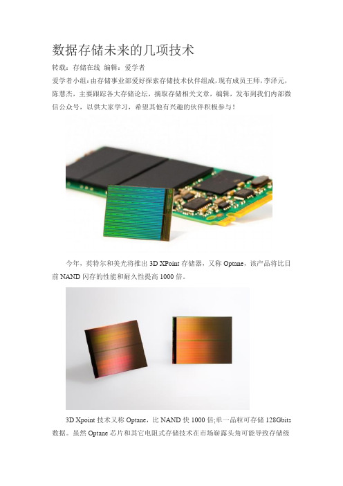
数据存储未来的几项技术转载:存储在线编辑:爱学者爱学者小组:由存储事业部爱好探索存储技术伙伴组成,现有成员王师,李泽元,陈慧杰,主要跟踪各大存储论坛,摘取存储相关文章,编辑,发布到我们内部微信公众号,以供大家学习,希望其他有兴趣的伙伴积极参与!今年,英特尔和美光将推出3D XPoint存储器,又称Optane,该产品将比目前NAND闪存的性能和耐久性提高1000倍。
3D Xpoint技术又称Optane,比NAND快1000倍;单一晶粒可存储128Gbits 数据。
虽然Optane芯片和其它电阻式存储技术在市场崭露头角可能导致存储级内存取代昂贵的DRAM适用许多应用程序,但它不会便宜太久。
这就给持续NAND闪存的发展留了门。
进入3D NAND闪存时代,三星,英特尔/美光,东芝和其它厂商始终认为容量会增加,价格会下压。
最终,3D NAND甚至会令消费者相信SSD能和HDD 一样实惠。
“很快闪存会比旋转介质更便宜,”闪迪公司存储技术部执行副总裁Siva Sivaram如是说。
与此同时,希捷已经展示了采用热辅助磁记录(HAMR)技术的HDD,能实现每平方英寸10Tbits以上的数据密度。
这比现有最高密度的HDD磁录密度高出10倍。
2017年,希捷预期与设备制造商合作展示HAMR产品,适用于数据中心应用,2018年预计开始走向更广阔的市场。
而这些近期的技术进展不过是持续迫使创新以满足新一轮存储需求竞逐中的冰山一角。
存储一直被念紧箍咒早在2000年,HDD公司就出现了容量限制问题,东芝和希捷将盘片上数据位从平铺变成垂直排列。
而从水平磁记录到垂直磁记录的改变提高了HDD几乎10倍的容量。
2013年,HDD行业再次面临容量限制,希捷模仿屋顶叠瓦式结构将数据磁道重叠,容量提了25%;然后2014年,HGST推出充氦硬盘,容量又拔高50%。
在非易失存储领域,容量瓶颈事件也时有发生,从SLC NAND闪存升为MLC NAND,MLC NAND一头走到黑的时候,三星又抛出了3D NAND的挂牌,英特尔/美光和东芝迅速跟进,将NAND单元堆栈到48层之高。
运算放大器的稳定性(01)
运放稳定性第1部分(共15部分):环路稳定性基础作者:Tim Green ,TI 公司Burr-Brown 产品战略发展经理1.0 引言本系列所采用的所有技术都将“以实例来定义”,而不管它在其他应用中能否用普通公式来表达。
为便于进行稳定性分析,我们在工具箱中使用了多种工具,包括数据资料信息、技巧、经验、SPICE 仿真以及真实世界测试等,都将用来加快我们的稳定运放电路设计。
尽管很多技术都适用于电压反馈运放,但上述这些工具尤其适用于统一增益带宽小于20MHz 的电压反馈运放。
选择增益带宽小于20MHz 的原因是,随着运放带宽的增加,电路中的其他一些主要因素会形成回路,如印制板 (PCB) 上的寄生电容、电容中的寄生电感以及电阻中的寄生电容与电感等。
我们下面介绍的大多数经验与技术并非仅仅是理论上的,而且是从利用增益带宽小于20MHz 的运放、实际设计并构建真实世界电路中得来的。
本系列的第1部分回顾了进行稳定性分析所需的一些基本知识,并定义了将在整个系列中使用的一些术语。
9Data Sheet Info 9Tricks 9Rules-Of-Thumb 9Tina SPICE Simulation9TestingGoal:EASILY Tricks & Rules-Of-Thumb apply for Voltage FeedbackOp Amps, Unity Gain Bandwidth <20MHzTo learn how to analyze and design Op Amp circuits for guaranteed Loop Stability using Data Sheet Info, Tricks, Rules-Of-Thumb, Tina SPICE Simulation, and Testing.Note:图1.0 稳定性分析工具箱图字(上、下):数据资料信息、技巧、经验、Tina SPICE 仿真、测试;目的:学习如何用数据资料信息、技巧、经验法则、Tina SPICE 仿真及测试来“更容易地”分析和设计运放,以确保环路稳定性;注:用于统一增益带宽小于20MHz 的电压反馈运放的技巧与经验法则。
pixel_shift原理__理论说明

pixel shift原理理论说明1. 引言1.1 概述本篇文章旨在探讨pixel shift原理,并对其进行理论说明。
Pixel shift技术是一种数字相机采用的高级图像处理技术,通过微小的传感器移动和像素位移来改善图像质量,提高分辨率和细节表现力。
本文将介绍该技术的原理、工作原理解析以及应用领域与优势。
1.2 文章结构本文共分为五个部分来阐述pixel shift原理。
首先,在引言部分简要阐述了全文内容概要。
接下来,在"2. pixel shift原理"部分,我们将详细介绍该技术的原理、工作原理解析以及应用领域与优势。
然后,在"3. 正文部分一"中,我们将着重讲述一些与pixel shift相关的重要要点;而在"4. 正文部分二"中,我们将继续探讨更多关键要点。
最后,在"5. 结论及展望"中,文章将对所述内容进行总结,并展望未来对该技术的研究方向。
1.3 目的撰写这篇长文的目的是为了帮助读者更好地了解并掌握pixel shift原理。
通过深入剖析其工作原理,读者将能够更全面地认识该技术,并在实际应用中发挥充分的优势。
本文的目标是向读者提供清晰易懂的解释和说明,以便促进对pixelshift原理的学习和进一步研究。
2. pixel shift原理:2.1 原理介绍:pixel shift是一种通过微小平移图像传感器来提高图像质量和分辨率的技术。
它通过在连续的几个曝光中将图像传感器稍微移动,然后将这些不同位置的图像合并起来,从而产生更加细致、清晰的图像。
2.2 工作原理解析:当相机启用pixel shift模式时,首先进行初始曝光以捕捉基准图像。
然后,在接下来的几次拍摄中,通过控制图像传感器微小地移动(通常为一个或半个像素),每次都进行一次曝光。
这样就形成了多张略有不同位置的照片。
在取得这些拍摄后,相机软件会自动将这些图片进行对齐,并利用差异部分进行插值合成。
- 1、下载文档前请自行甄别文档内容的完整性,平台不提供额外的编辑、内容补充、找答案等附加服务。
- 2、"仅部分预览"的文档,不可在线预览部分如存在完整性等问题,可反馈申请退款(可完整预览的文档不适用该条件!)。
- 3、如文档侵犯您的权益,请联系客服反馈,我们会尽快为您处理(人工客服工作时间:9:00-18:30)。
OPTI 696C Practical Optics SeminarTerm paperTaeyoung ChoiADE Phaseshift is a company that specializes in metrology, inspection and process control. ADE Phaseshift was merged with KLA-Tencor in 2006 and now became an ADE division of KLA-Tencor. The application fields are silicon wafer manufacturing, semiconductor manufacturing, magnetic data storage, and optics/precision-engineered surfaces. The consumers of their instruments are semiconductor equipment manufacturers, wafer manufacturers, data storage companies like Seagate and Hoya, precision-optics companies, or tribology companies like Alcoa, GE, Apple. The competitors are Veeco, Zygo, Taylor Hobson, Fogale, SNU precision and so forth.The presentation and tour were based on some of their best-selling metrology instruments for small systems and large systems. The technology developed for small optical systems is used for producing large optics metrology instruments.1. Optical profiler (MicroXAM)MicroXAM is a 3D non-contact surface profiler for surface analysis and roughness. An Michelson-type optical profilometer uses two low magnification (for 2.5X, 5X) objective lenses. One is focused on the reference and the other focused on the sample. A Mirau interferometer is used with high magnification (>10X) objective lenses. The advantage of the Mirau type is that it is a common path after the beamsplitter, and the disadvantage is that the objective lens should have a long working distance to have a beamsplitter. [1] A beamsplitter and a reference plate are placed inside the microscope objective as shown in Fig. 1. There are two operation modes: phase shifting interferometry (PSI) and vertical step interferometry (VSI). In general, PSI has accuracy, but limited dynamic range. [2] In phase-shifting interferometers, the height difference between two adjacent data points must be less than λ/4, because of π-phase ambiguities. VSI overcomes this phase ambiguity problem by using multiple wavelengths or preferably white light and sensingthe coherence peak during vertical scan. Therefore, VSI provides wide dynamic range with reduced vertical resolution.In MicroXAM, the PSI mode uses a narrow bandpass-filtered colored light, has the maximum height of about 200nm, and has a vertical resolution of 0.01nm. On the other hand, the VSI mode uses a white light and has the max. vertical scanning range of about 2mm. The vertical resolution of VSI is 1nm, and the step size is around 10um. The lateral resolution is about 1um, but it depends on numerical aperture (NA) of the objective lens used.Fig. 1 Mirau interferometer used for high magnification objective lenses. A beam splitter and a reference are placed inside the microscope objective.2. MiniFiz Laser interferometer (MiniFiz )A MiniFiz is a Fizeau interferometer for testing flat, concave or convex surfaces and wavefront transmission by phase shifting, as shown in Fig. 2. Phase shift for small optics is achieved with a PZT. For large optics, however, they use wavelength shifting instead of a PZT. Wavelength shifting is realized using an external cavity laser diode with λ=635nm and P=1mW. A grating in the laser is rotated by a PZT to tune the wavelength. The amount of tuning required to introduce a certain amount of optical path length difference (OPD) is calculated by dividing the wavelength, λ, by the OPD. That is, OPD λ∆λ= An external cavity diode laser (ECDL) used for phase shifting in MiniFiz is furtherstudied. Figures 2(a) and (b) schematically show external cavity diode lasers (ECDLs) inLittrow and Littman configurations, which are the most common types of ECDLs that use a simple diffraction grating as a tunable filter. [3,4] In both types of ECDLs, the front facet of the laser diode is antireflection(AR)-coated with one or more dielectric layers in order to suppress the internal cavity modes. In the Littrow configuration ECDL, the emitted light from the AR-coated front facet is collimated and directed to the reflection grating. The grating is aligned to return its first order diffraction beam to the laser cavity. The zeroth order beam is used as output. So, the wavelength of the output beam is determined by the total cavity length, which consists of the cavity of the original laser chip and the external cavity between the laser front facet and the grating surface. Rotating the grating about an axis changes not only the external cavity length, but also the incident angle of the beam on the grating, which shifts the external cavity modes and the peak wavelength of the filter. Then, the output wavelength is forced to occur where one of the external cavity modes matches the filter peak. One drawback of the Littrow configuration is that the rotation of the grating results in an angular change of the output beam or a parallel shift when a beam correction mirror is placed on the output side of the grating, as shown in Fig. 2 (b). The Littman configuration ECDL is similar to the Littrow ECDL, except for the fact that it has a larger incidence angle onto the grating and tunes the wavelength by rotating the mirror with the grating fixed. So, the output beam is in a fixed direction, regardless of mirror rotation for tuning.MiniFiz can measure surface flatness, homogeneity, index variation. In addition, it can measure a plane parallel plate that has the pseudo-reflection from the back surface when using the wavelength-shifting technique. The reflected light from the second surface will be filtered out in an algorithm. Another unique feature is saturation insensitivity in CCD pixels. With CCD pixels saturated, we can still get accurate measurements of a surface. An algorithm in the analysis procedure solves the pixel saturation problem.Reference[1] B. Bhushan, J. C. Wyant, and C. L. Koliopoulos, "Measurement of surface topography of magnetic tapes by Mirau interferometry," Appl. Opt. 24, 1489- (1985) [2] J. C. Wyant, OPTI513R classnote on “White light interferometry,”/jc wyant/pdf/Meeting_papers/WhiteLight Interferometry.pdf [2] Zorabedian, P., “Tunable external cavity semiconductor lasers,” in Tunable Lasers Handbook, F. J. Duarte, Ed. (Academic Press, San Diego, 1995).[3] Sacher Lasertechnik Group: /ExternalCavity.php。