a novel dual-band circularly polarized wide beam quadrifilar helix antenna
圆极化TE_(11)输出模式旋向可在线切换的相对论磁控管模拟研究

旋 圆 极 化 TE11 模 式 且 模 式 纯 度 达 到 99% 以 上 ; 当 外 加 轴 向 磁 场 与 微 波 轴 向 输 出 方 向 反 向 时 , 该 器 件 的 输 出 模 式
即 可 在 线 切 换 为 左 旋 圆 极 化 TE11 模 式 , 而 其 他 输 出 性 能 基 本 保 持 不 变 。
100 200 300 400 z/mm
Fig. 1 Schematic diagram of the longitudinal profile of the RM 图 1 RM 纵剖面结构
波导张角 θc2=55°。该模型整体结构可分为四个部分,即 A 部分:用于电功率输入的同轴结构;B 部分:用于束波 相互作用的谐振腔结构;C 部分:用于微波提取和模式转换的扇形波导结构;D 部分:用于微波输出的同轴结构。
Shi Difu, Qian Baoliang
(College of Advanced Interdisciplinary Studies, National University of Defense Technology, Changsha 410073, China)
Abstract: A relativistic magnetron with online switchable rotation direction of a circularly polarized TE11 output mode is proposed. In the device, the same cavity magnetron is adopted as the beam-wave interaction structure, the all-cavity extraction structure is adopted as the output structure, and the Helmholtz coils system is adopted as the magnetic system. In this paper, the output mode components of the device are theoretically analyzed by the mode excitation theory of all-cavity extraction structure, and the performance of the device is investigated by Particle in Cell simulation. Simulation results show that when the applied voltage is 770 kV and the applied magnetic field that has the same direction with the output microwave is 0.2 T, the device that operates at 5π/6 mode can output a right circularly polarized TE11 mode with the mode purity of more than 99%, the operating frequency of 2.35 GHz and the output power of 3.86 GW, corresponding to the power conversion efficiencyof 55.5%. When the direction of the applied magnetic field is reversed, the rotation direction of the right circularly polarized TE11 mode can be online switched to the left in the condition of keeping other performance of the device.
Hayati_et_al-2013-Microwave_and_Optical_Technology_Letters
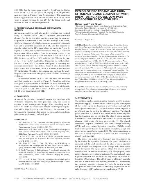
2.88GHz.For the lower mode with C¼0.6pF and the higher mode with C¼5pF,the effects of varying/on CP perform-ance are given in Figures4and5,respectively.The simulation results suggest that an axial ratio of less than2dB can be found when/ranges between10and25 for the lower mode and between12and16 for the higher mode.3.RECONFIGURABLE DESIGN AND EXPERIMENTAL RESULTSAn antenna prototype with electrically switching was realized using a varactor diode(BB837,Siemens Semiconductor Group).For the dc bias(V0)used for controlling the varactor, its positive is connected to the feed line through a RF choke, which is composed of a high-impedance meandered microstrip line and a grounded capacitor of1nF,and the negative is directly linked to the RF ground plane,as shown in Figure1. Figure6exhibits the experimental results when V0is switched between two different values.From the measured results,it can be seen that the frequency with minimum axial ratio is1.83 GHz for the case of V0¼28V and it is2.96GHz for the case of V0¼6V.The CP bandwidths,determined by3dB axial ra-tio,are2.7and3.3%at the lower and higher CP operating fre-quencies,respectively.In addition,Figure6also demonstrates that a return loss of less than10dB is achieved within the two CP bandwidths.Therefore,the antenna can perform the dual-frequency operation with a frequency ratio of about1.6through switching.The radiation patterns at1.83and2.96GHz are measured and their results are plotted in Figure7.Broadside radiation with good CP performance is observed for each operating fre-quency,and the polarization in the plane of z>0is left-handed. The peak gain at1.83GHz is about3.3dBic and it is merely 0.2dB lower than that at2.96GHz.4.CONCLUSIONA design for circularly polarized annular slot antennas with switchable frequency has been presented.Only one diode is required in the reconfigurable design.With controlling the dc bias of the diode,the antenna can perform dual-frequency opera-tion with a high frequency ratio.Moreover,the antenna at the two operating frequencies has almost the same radiation pattern, polarization performance,and peak gain.REFERENCES1.Y.K.Jung and B.Lee,Dual-band circularly polarized microstripRFID reader antenna using metamaterial branch-line coupler,IEEE Trans Antennas Propag60(2012),786–791.2.Nasimuddin,Z.N.Chen,and X.Qing,Dual-band circularly-polar-ized S-shaped slotted patch antenna with a small frequency ratio, IEEE Trans Antennas Propag58(2010),2112–2115.3.J.Y.Sze,C.I.G.Hsu,and J.J.Jiao,CPW-fed circular slot antennawith slit back-patch for2.4/5GHz dual-band operation,Electron Lett42(2006),563–564.4.Y.L.Zhao,Y.C.Jiao,G.Zhao,Z.B.Weng,and F.S.Zhang,Anovel polarization reconfigurable ring-slot antenna with frequency agility,Microwave Opt Technol Lett51(2009),540–543.5.N.Jin,F.Yang,and Y.Rahmat-Samii,A novel patch antenna withswitchable slot(PASS):dual-frequency operation with reversed cir-cular polarizations,IEEE Trans Antennas Propag54(2006), 1031–1034.6.T.Y.Lee and J.S.Row,Frequency reconfigurable circularly polar-ized slot antennas with wide tuning range,Microwave Opt Technol Lett53(2011),1501–1505.V C2013Wiley Periodicals,Inc.DESIGN OF BROADBAND AND HIGH-EFFICIENCY CLASS-E AMPLIFIER WITH pHEMT USING A NOVEL LOW-PASS MICROSTRIP RESONATOR CELLMohsen Hayati1,2and Ali Lotfi11Electrical Engineering Department,Faculty of Engineering,Razi University,Tagh-E-Bostan,Kermanshah-67149,Iran; Corresponding author:mohsen_hayati@2Computational Intelligence Research Centre,Razi University,Tagh-E-Bostan,Kermanshah-67149,IranReceived31August2012ABSTRACT:In this article,a high-efficient class-E amplifier design with low voltage and broadband characteristics using a novel Front Coupled Tapered Compact Microstrip Resonant Cell is presented.The proposed micorstrip resonator is used as the harmonic control network in order to suppress higher order harmonics,which obtained the optimized impedance matching for the fundamental and harmonics.The class-E amplifier is realized from0.7to1.8GHz,and obtained the power added efficiency of72.5–77.5%.The maximum value of Power added efficiency(PAE)is79.7%with11-dBm input power at1.5GHz. The designed class-E amplifier using the proposed harmonic control network gained15.34%increment in PAE,and25.6%reduction in the circuit size in comparison with the conventional class-E amplifier.The simulation and measurement results show the validity of the proposed design procedure of the broadband class-E amplifier using a novel microstrip resonator cell.V C2013Wiley Periodicals,Inc.Microwave Opt Technol Lett55:1118–1118,2013;View this article online at .DOI10.1002/mop.27490Key words:switch mode;class-E amplifier;tapered cell;microstrip resonant cell;high efficiency;power added efficiency;zero voltage switching;zero voltage derivative switching1.INTRODUCTIONThe modern wireless communication systems need to consume the power supply.The main factor in reducing the consumption of the power supply is designing a low-voltage and high-effi-ciency power amplifier[1].The switch mode power amplifier is an efficient way for solving the efficiency problem.The class-E power amplifier is a kind of the switch mode power amplifier that the transistor acts as a switch.The class-E power amplifier is tuned by a shunt capacitance.This type of the power amplifier obtained100%drain efficiency theoretically[2].The class-E amplifier’s response conditions are zero voltage switching (ZVS)and zero voltage derivative switching(ZVDS),which lead to zero power loss in the transistor.Therefore,a high-effi-ciency power amplifier is obtained[3].The shunt capacitance in the class-E power amplifier has a main roll for achieving the class-E conditions[4].The power loss in the lower frequency can be neglected,but by increasing the operation frequency,the power dissipation is increased and the ideal operation of the class-E power amplifier will be missed.The antiphase of the voltage and current wave-forms throughout the signal period,obtain the class-E power amplifier with the maximum efficiency[5].This purpose can be achieved using a wave shaping network.The conventional class-E power amplifier load resistance is very much lower than the transistor ON-resistance.This effect leads to efficiency degrada-tion and a narrowband load matching network[6].Furthermore, the transistor parasitic resistance for both the switch on-state and parasitic inductance leads to efficiency degradation in the radio frequency(RF)and microwave applications[7,8].The optimum operation of the class-E power amplifier and the solution to the mentioned drawbacks can be obtained using two main methods:namely active device selection and circuit configuration[9].The class-E amplifier has various configura-tions such as the cascade[10]and push–pull[11].The cascade class-E configurations can double the maximum permissible drain voltage,and the push–pull class-E configuration increases the output power and decrease the harmonic distortion with high efficiency.A new topology for the class-E amplifier is proposed as an inverse class-E amplifier,which has inductive reactance [12].The inverse class-E amplifier has higher load resistance and lower peak switch voltage in comparison with the class-E amplifier.Also,because of the abruption of the device output inductances,the value of the inductance in the load network is decreased.However,the inverse class-E amplifier can be used only for the small to medium power applications.Therefore,to solve this drawback,the power combining methods have been used[13].Although,this method results in obtaining the inverse class-E amplifier for higher power application,but the circuit configuration and the design procedure are complicated with the circuit size increment because of using two power amplifier circuits.The class-E power amplifier is a high-efficiency power am-plifier for the microwave application,which is implemented using the transmission line as the harmonic control network at the output of the amplifier circuit[14].Furthermore,instead of the RF choke(RFC)a section of the transmission line is used.The transmission line has been used in the class-E power amplifier using LDMOS[15],GaN HEMT[16–19],SiC MES-FET[20],and LDMOSFET[21]as the harmonic control net-work increasingly,because of the simplicity of its structure and high rejection of harmonics.Therefore,the class-E amplifier configuration and operation are the best candidates for the design of the amplifier for the modern microwave communica-tion systems[22,23].Consequently,designing of the load network as the harmonic control network for suppression of harmonics in order to obtain a high-efficiency power amplifier is the main challenge of the switch mode power amplifiers.The designing of the class-E power amplifiers using various microstrip structures has been proposed such as a defected ground structure[24],an asymmet-rical spur-line[25],and composite right/left-handed transmission lines[26].The narrowband load network and low efficiency remain as the main challenge to the class-E power amplifier using the conventional microstrip transmission line[27].A compact microstrip resonant cell(CMRC)is a one-dimen-sional photonic band gap incorporating the microstrip transmis-sion line,which is,first,proposed in[28].The CMRC structure exhibits high rejection of the harmonics with the compact circuit size in comparison with the conventional micorstrip transmission lines.Therefore,it is used for the linearization and efficiency in-crement of the microwave power amplifiers[29,30].The appli-cation of the conventional CMRC is limited to obtain a high-ef-ficiency switch mode amplifier,as a result of the high insertion loss in the passband and restricted stopband.The front coupled tapered CMRC(FCTCMRC)is proposed in[31]for the implan-tation of a low-passfilter with high and wide rejection in the stopband with the compact circuit size in comparison with the conventional CMRC.Therefore,it can be widely used for designing the high-efficiency and broadband switch mode power amplifier because of high and wide suppression of harmonics.In this article,the harmonic suppression of the class-E ampli-fier using a novel FCTCMRC as the harmonic controller net-work is explored.A class-E amplifier with higher efficiency at a wider bandwidth in comparison with the conventional amplifiers is achieved.The proposed class-E power amplifier is designed and simulated for a frequency of1.5GHz using the micorstrip resonator structure.The measurement results of the proposed power amplifier validate our design procedure and simulation results.2.CLASS-E AMPLIFIER FUNDAMENTAL AND DESIGN THEORY2.1.Class-E Amplifier OperationThe basic circuit configuration of the class-E amplifier and switch waveforms are shown in Figures1(a)and1(b),respec-tively.The class-E amplifier consists of the switch device,shunt capacitance,series-tuned load network L-C,and an ideal RFC. The switch-on duty ratio is assumed to be50%in designing the class-E amplifier.This value of the duty ratio leads to optimum operation of the class-E amplifier for obtaining high efficiency [32].For an ideal class-E operation,three requirements for the drain voltage and current should be met[2]:1.The rise of the voltage across the transistor at turn-offshould be delayed until the transistor is off.2.The drain voltage should be brought back to zero at thetime of the transistor turn-on.3.The slope of the drain voltage should be zero at the timeof the transistor turn-on.Therefore,the class-E power amplifier is constructed based on two conditions as ZVS and ZVDS.These conditions are as follows:v s hðÞjh¼p¼0;(1)dv s hðÞd hh¼p¼0;(2)where v s(y)is the switch voltage,and y¼x t.The quality fac-tor of the output series resonant circuit is assumed infinite. Therefore,the output current is sinusoidal asi oðhÞ¼I m sinðhþuÞ:(3)In the time interval0y<p,the switch device is in the on-state,therefore,using Kirchhoff’s current law at the switch,we havei sðhÞ¼I dc1þa sin hþuðÞðÞ:(4)This is the currentflow through the shunt capacitance in the switch-off state.Therefore,the voltage across the switchisFigure1(a)The basic circuit of the class-E amplifier.(b)The class-E switch voltage and current waveformv sðtÞ¼1C sZ ti sðt0Þdt0¼I dcx C s1þa cos x tþuðÞÀcos uðÞðÞ:(5)Applying the class-E ZVS and ZVDS conditions to Eqs.(4)and (5),the value of a and u can be obtained asa¼ffiffiffiffiffiffiffiffiffiffiffiffiffi1þp24r;(6)u¼ÀtanÀ12p8>:9>;:(7)The drain voltage waveform is shaped by the harmonics so that the drain voltage and the slope of the drain voltage is zero when the transistor is in the on-state.The reactance for all harmonics is negative and comparable in magnitude to the fundamental fre-quency load resistance.The ideal class-E amplifier requirements are difficult to meet.So,we often only tuned the second and third harmonics to get the suboptimum class-E power amplifier solution.The analysis is performed considering just the output network behavior,thus neglecting input signal required to oper-ate the active device as an ideal switch.The optimal fundamental load by the Fourier-series expan-sion analysis in[7]used for achieving the perfect class-E opera-tion can be determined asZ E;f0¼0:28x C Pe49 :(8)This impedance is inductive.On the other hand,for the ideal operation of the class-E power amplifier the impedances at the higher order harmonics are infiniteZ E;fn¼1;for n!2:(9)From(8)the nominal class-E amplifier shunt capacitance C is defined byC¼0:1836x0R:(10)In order to achieve the maximum operation frequency of the class-E amplifier,the device output capacitance should be equal to Eq.(10).The matching network for the class-E power ampli-fier using a low-pass Chebyshev-form impedance transformer is proposed in[7].Therefore,the synthesis of the load network is done using a short circuit,and open circuit stubs instead of lumped capacitors in the load network for unwanted harmonics.2.2.Design of a Class-E Amplifier Using a pHEMTAchieving the optimum load is the main factor to obtain high efficiency when designing the class-E power amplifier.On the other hand,the optimum load is varied with the operating fre-quency as in Eq.(8).Therefore,designing of the load network, which can operate in the wide frequency range,is needed for designing the class-E power amplifier with the optimum condi-tions.The maximum operation frequency of the class-E power amplifier is restricted by the shunt capacitance.The shunt capac-itance consists of the transistor output capacitance and the exter-nal capacitance.Thus,the optimum operating frequency of the class-E power amplifier is achieved by selecting a transistor with lower output capacitance.On the other hand,the power loss is caused by ON-resistance of the transistor[33].Therefore, the active device with lower ON-resistance is preferred for designing the high-efficiency class-E power amplifier.We selected an ATF-34143pHEMT because of its lower ON-resist-ance and lower shunt parasitic capacitance,which provides lower power dissipation and optimum operation frequency using external capacitance,respectively.The circuit topology of the conventional class-E amplifier is shown in Figure2(a).It is designed using the design procedure,which is presented in[2, 3].The value of elements for an ideal class-E power amplifier is tabulated in Table1.In the design of the class-E power ampli-fier,it is assumed that the value of the DC-feed is infinitive,but in real implementation this value isfinite,and we used the half wavelength microstrip transmission line for the DC-feed.In the conventional class-E amplifier,using lumped elements, the second harmonic is located within the pass band.Therefore, the bandwidth is limited to one octave.In order to solve this drawback,one way is designing a multiple matching network for various bands and using switching element.This way leads to complexity of the amplifier circuit and degradation of the efficiency.The use of the micorstrip transmission line is a low-cost and simple way for designing the class-E amplifier with wide band and high-efficiency characteristics.We used the design proce-dure in Section2.1and designed the matching network for the amplifier as shown in Figure2(b).The values of the transmis-sion lines dimensions are given in Table2.The class-E ampli-fier is designed on RT/Duroid5880,a substrate with dielectric constant of2.2,height of15l l,and loss tangent of0.0009.Figure2Idealized class-E power amplifier:(a)lumped elements and(b)transmission lineTABLE1Element Design for the Nominal Class-E AmplifierC i1(pF)C i2(pF)C o1(pF)C o2(pF)C e(pF)C g1(pF)C g2(pF)C d1(pF)C d2(pF)L i1(nH)L o1(nH)L o2(nH) Theoretical10010010010 4.2221000.50.2312 4.7 3.33.FRONT COUPLED TAPERED CMRC CHARACTERISTICSA novel FCTCMRC is proposed in [31],for the first time,which is used to synthesize a low-pass filter with high and wide rejec-tion in the stopband.This microstrip structure exhibits bandstop characteristics and slow wave effects,which are used in the stopband extension and the circuit size reduction,respectively.The schematic and equivalent circuit of the resonator is shown in Figures 3(a)and 3(b),respectively.The proposed FCTCMRC has symmetrical topology.Therefore,the even–odd mode [34]can be used to simplify the analysis as shown in Figures 3(c)and 3(d).Consequently,theresonant condition for the odd-mode in Figure 3(c)is obtained by equating the input admittance Y o in of the proposed resonator to zero yields:Z 112x C 1ÀZ 1tan h 1 ÀZ 2tan h 2Z 1þtan h 12x C 1¼0:(11)Using the similar procedure,the even-mode resonant frequencies areobtained by equating the even admittance Y e in to zero as follows:Z 2tan h 1þZ 1tan h 2¼0:(12)The transmission zeros of the equivalent circuit for the proposed FCTCMRC,which is shown in Figure 3(a),is obtained whenY o in ¼Y ein asZ 2sin 2h 2þZ 1sin 2h 1¼cos 2h 1x C 1:(13)Therefore,the resonator characteristics for tuning transmission zeroes in the stopband can be achieved by the length and width of the tapered cells as shown in Figures 4(a)and 4(b).The pro-posed structure is optimized by an EM-simulator (ADS).The obtained dimensions are as follows:L t1¼2:58;L 2¼1:94;L 3¼2:7;W t1¼2:71;W t2¼5:6;W 1¼0:1;W 2¼0:56;L 3¼0:75;L f ¼2:36;W f ¼0:25all are in millimeter ðmm Þ:TABLE 2The Value of the Conventional Transmission Line for the class-E AmplifierTL 1TL 2TL b1TL 3TL 4TL 5TL b2Width (mm) 4.730.940.620.71 1.24 4.210.72Length (mm) 6.319.7262.3137.2318.4264.3Figure 3(a)Schematic of the proposed resonator.(b)Equivalent cir-cuit.(c)Odd-mode.(d)EvenmodeFigure 4(a)Changing of the transmission zeros with the width of tapered cell W t1.(b)Changing of the transmission zeros with the length of tapered cell L t .(c)Simulation and measurement results of the proposed harmonic control network.(d)Simulation input impedance of the FCTCMRCThe proposed FCTCMRC is fabricated,and the measurement is performed using an Agilent N5230A Network Analyzer.The simulation and measurement results of the proposed FCTCMRC are shown in Figure 4(c).As it is shown,it has an attenuation level À43and À33.1dB at 3.0and 4.5GHz,respectively.Therefore,the high suppression for the second and third har-monics is obtained.The insertion loss from DC to 2.39GHz is lower than À0.1dB.The simulation of the input impedance of the proposed CMRC for the fundamental and harmonics is shown in Figure 4(d).As it is observed,the harmonic impedan-ces are relatively open in comparison with the fundamental im-pedance.Consequently,it can be used as the matching network with high performance and low circuit complexity.4.CIRCUIT DESIGN AND IMPLEMENTATIONThe highly efficient and compact size class-E amplifier is designed and implemented for a 1.5-GHz band using an ATF-34143pHEMT.The proposed circuit is simulated using an Agi-lent’s Advanced Design System (ADS),and fabricated on an RT/Duroid 5880substrate.The active device is biased at V d ¼3V and V g ¼À0.7V.The FCTCMRC is used as the harmonic control network (HCN)at the output of the active device.The proposed HCN absorbed the parasitic reactance and capacitance of the active device.Therefore,it does not need to any lumped elements in series or parallel with the transistor to compensate the parasitic elements.The circuit schematic diagram of the designed class-E amplifier is shown in Figure 5(a).Moreover,the photograph of the fabricated circuit is shown in Figure 5(b).The RFC is realized using the microstrip transmission line (TLb2)with the quarter wavelength at a frequency of 1.5GHz.The input matching elements consist of two series and parallel open stubs.The dimensions of the tapered cells and transmission lines in the HCN are tuned in order to optimize harmonic termi-nation in the implemented amplifier circuit.The design and implementation of the output matching networks using the FCTCMRC as low-pass topology has been done from 0.7to 1.8GHz.The voltage and current waveforms of the designed class-E amplifier are shown in Figure 5(c).The switch is open for the time interval,0.2–0.4ns and the current through it is near zero.The switch is closed during the time interval 0.6–0.8ns,and the voltage across it is near to zero.The class-E ZVS and ZVDS conditions in the switch turn-off state are obtained.Therefore,the high-efficiency class-E amplifier is achieved.The input signal is generated using an Agilent E4433B signal generator,and the measurement is done by an E4440A PSA se-ries spectrum analyzer.The simulated and measured output power and gain for P in ¼11dBm (input power)are shown in Figure 6(a).The maximum output power at 1.5GHz with P in ¼11dBm is 25.3dBm,and the related gain is 14.3dB.The con-ventional class-E amplifier without CMRC has an output power of 18.5dBm and gain of 7.5dB.The class-E amplifier using CMRC has 36.7%output power improvement in comparison with the one without CMRC.The simulation and measurement results for the PAE at P in ¼11dBm (input power)is shown as a function of the operating frequency in Figure 6(b).The highest value of PAE at a fre-quency of 1.5GHz was 79.7%.The value of the PAE is 69.1%for the conventional class-E amplifier without CMRC.There-fore,the proposed class-E amplifier using the novel CMRC has 15.34%PAE improvement in comparison with the one without CMRC.The output power of the conventional class-E amplifier is decreased as the operating frequency is increased.As shown in Figure 6(a),this decrement is considerable when the operating frequency is more than 1.2GHz.Therefore,the conventional class-E amplifier has a drawback for the broadband applications.The designed class-E amplifier has 25.6%circuit size reduction in comparison with the conventional class-E amplifier.5.CONCLUSIONThe class-E amplifier with high efficiency and broadband char-acteristics has been designed and implemented.A novel and simple load-matching technique for the low-voltage microwave class-E amplifier using a front-coupled taperedcompactFigure 5The pHEMT class-E amplifier.(a)Circuit configuration.(b)A photograph of fabricated amplifier.(c)Simulated switch voltage and current waveforms.[Color figure can be viewed in the online issue,which is available at ]microcstrip resonant cell has been presented.The proposed am-plifier achieved an output power of 25.3dBm,a power added efficiency of 79.7%,and a gain of 7.5dB at input power of 11dBm.It has high-efficiency performance over a significant band-width form 0.7to 1.8GHz (88%).The proposed compact micro-strip resonant cell as the harmonic control network exhibited 15.34%improvement in PAE and 25.6%reduction in the circuit size in comparison with the conventional class-E amplifier.The extremely low insertion loss at the fundamental frequency and size reduction characteristics can be used in the design of the class-E amplifier with higher output power and smaller size,which are required in the broadband application.REFERENCES1.S.C.Cripps,Advanced techniques in RF power amplifiers design,Artech House,Norwood,MA,2002.2.N.O.Sokal and A.D.Sokal,Class E—A new class of high-effi-ciency tuned single-ended switching power amplifiers,IEEE J Sol-id-State Circuits 10(1975),168–176.3.F.H.Raab,Idealized operation of the class E tuned power ampli-fier,IEEE Trans Circuits Syst 25(1977),725–735.4.R.E.Zulinski and J.W.Steadman,Class E power amplifiers and frequency multipliers with finite DC-feed inductance,IEEE Trans Circuits Syst 34(1987),1074–1087.5.R.Negra,F.M.Ghannouchi,and W.Bachtold,Study and design optimization of multi-harmonic transmission-line load networks for class-E and class-F K-band MMIC power amplifiers,IEEE Trans Microwave Theory Tech 55(2007),1390–1397.6.K.L.R.Mertens and M.S.J.Steyaert,A 700-MHz 1-W fully differ-ential CMOS class-E power amplifier,IEEE J Solid-State Circuits 37(2002),137–141.7.T.B.Mader and Z.B.Popovic,The transmission line high-effi-ciency class-E amplifier,IEEE Microwave Guided Wave Lett 5(1995),290–292.8.T.Suetsugu and M.K.Kazimierczuk,Design procedure for lossless voltage-clamped class E amplifier with a transformer and a diode,IEEE Trans Power Electron 20(2005),56–64.9.H.J €a ger,A.V.Grebennikov,E.P.Heaney,and R.Weigel,Broad-band high-efficiency monolithic In-GaP/GaAs HBT power ampli-fiers for wireless applications,Int J RF Microwave Comput Aided Eng 13(2003),496–510.10.A.Mazzanti,rcher,R.Brama,and F.Svelto,Analysis of reli-ability and power efficiency in cascode class-E PAs,IEEE J Solid--State Circuits 41(2006),1222–1229.11.S.C.Wong and C.K.Tse,Design of symmetrical class-E poweramplifiers for very low harmonic-content applications,IEEE Trans Circuits Syst I,Reg Papers 52(2005),1684–1690.12.T.Mury and V.F.Fusco,Inverse class-E amplifier with transmis-sion line harmonic suppression,IEEE Trans Circuits Syst I,Reg.Papers 54(2007),1555–1561.13.T.Mury and V.F.Fusco,Power combining techniques into unbal-anced loads for class-e and inverse class-e amplifiers,IET Micro-wave Antennas Propag 2(2008),529–537.14.A.J.Wilkinson and J.K.A.Everard,Transmission-line load-networktopology for class-E power amplifiers,IEEE Trans Microwave Theory Tech 49(2001),1202–1210.15.J.Lee,S.Kim,J.Nam,J.Kim,I.Kim,and B.Kim,Highly effi-cient LDMOS power amplifier based on class-E topology,Micro-wave Optical Technol Lett 48(2006),789–791.16.Y.-S.Lee and Y.-H.Jeong,A high-efficiency class-E GaN HEMTpower amplifier for WCDMA applications,IEEE Microwave Wire-less Compon Lett 17(2007),622–624.17.H.G.Bae,R.Negra,S.Boumaiza,and F.M.Ghannouchi,High-ef-ficiency GaN class-E power amplifier with compact harmonic-sup-pression network,Proc 37th Europ Microwave Conf,2007,pp.1093–1096.18.Y.-S.Lee,M.-W.Lee,and Y.-H.Jeong,A 1-GHz GaN HEMTbased class-E power amplifier with 80%efficiency,Microwave Opt Technol Lett 50(2008),2989–2992.19.Y.-S.Lee,M.-W.Lee,and Y.-H.Jeong,A 40-W balanced GaNHEMT class-E power amplifier with 71%efficiency for WCDMA base station,Microwave Opt Technol Lett 51(2009),842–845.20.Y.S.Lee and Y.H.Jeong,A high-efficiency class-E power ampli-fier using SiC MESFET,Microwave Opt Technol Lett 49(2007),1447–1449.21.J.-H.Van,M.-S.Kim,S.-C.Jung,H.-C.Park,G.Ahn,C.-S.Park,B.-S.Kim,and Y.Yang,A high-frequency and high-power quasi-class-E amplifier design using a finite bias feed inductor,Micro-wave Opt Technol Lett 49(2007),1114–1118.22.R.Beltran,F.H.Raab,and A.Velazquez,High-efficiency out phas-ing transmitter using class-E power amplifiers and asymmetric combining,Microwave Opt Technol Lett 51(2009),2959–2963.23.C.Park,Y.Kim,H.Kim,and S.Hong,Fully integrated 1.9-GHzCMOS power amplifier for polar transmitter applications,Micro-wave Opt Technol Lett 48(2006),2053–2056.24.Y.C.Jeong,S.-G.Jeong,J.S.Lim,and S.W.Nam,A new methodto suppress harmonics using k /4bias line combined by defected ground structure in power amplifiers,IEEE Microwave Wireless Compon Lett 13(2003),538–540.25.L.Wang,W.Chen,P.Wang,X.Xue,J.Dong,and Z.Feng,Design of asymmetrical spur-line filter for a high power sic MES-FET class-E power amplifier,Microwave Opt Technol Lett 52(2010),1650–1652.26.M.Thian and V.Fusco,Design strategies for dual-band class-Epower amplifier using composite right/left-handed transmission lines,Microwave Opt Technol Lett 49(2007),2784–2788.27.Y.Qin,S.Gao,A.Sambell,and E.Korolkiewicz,Design of low-cost broadband class-e power amplifier using low-voltage supply,Microwave Opt Technol Lett 44(2005),103–106.28.Q.Xue,K.M.Shum,and C.H.Chan,Novel 1-D microstrip PBGcells,IEEE Microwave Wireless Comp Lett 10(2000),403–405.29.T.Yin,Q.Xue,and C.H.Chan,Amplifier linearization using com-pact microstrip resonant cell-theory and experiment,IEEE Trans Microwave Theory Tech 52(2004),927–934.Figure 6Comparison of the conventional amplifier simulation with the simulated and measured results of the proposed amplifier.(a)Output power and gain.(b)Power added efficiency (PAE %)。
用于Ka波段卫星通信的双频段圆极化无源相控阵天线

收 稿 日 期 :2023 - 08 - 10 基金项目:国家自然科学基金青年科学基金项目(62101276);江苏省高等学校基础科学(自然科学)研究项目面上项目(21KJB510002);南京信 息工程大学人才启动经费(1521082101016) : ( ); Foundation Item Youth Fund of the National Natural Science Foundation of China 62101276 Natural Science Foundation of the Jiangsu Higher Educa ( ); ( ) tion Institutions of China 21KJB510002 Startup Foundation of NUIST for Introducing Talents 1521082101016
, respectively in the transmitting and receiving frequency band and the axial ratio of the circular polarized beam is always below 3 dB , when the deflection is 60° and the cross polarization level is very low.
reconfiguration and beam scanning functions are achieved in the 29. 5 ~ 30 GHz transmission frequency band and 19. 7 ~ 20. 2 GHz
低RCS宽带磁电偶极子贴片天线设计

低RCS宽带磁电偶极子贴片天线设计张晨;曹祥玉;高军;李思佳;黄河【摘要】该文设计了一种低雷达散射截面(RCS)的宽带磁电偶极子贴片天线,其中印刷在介质板上的金属贴片为电偶极子,3个金属过孔连接辐射贴片与金属地板构成磁偶极子。
整个天线采用“T”型渐变馈电结构同时激励电偶极子与磁偶极子,天线的频带范围为7.81~13.65 GHz,覆盖了整个X波段。
实测和仿真结果表明,通过在磁电偶极子贴片天线底面采用开槽技术并优化开槽的形状、大小、位置等变量,在天线工作频带范围内实现了RCS的减缩,最大缩减量达到了17.9 dB,同时天线保持了增益稳定不变,E面、H面方向图一致的特性。
%A low Radar Cross Section (RCS) and broadband Magneto-Electric (ME) dipole patch antenna from 7.81 GHz to 13.65 GHz covering the whole X band is designed and fabricated. Metal patches printed on the substrate form the electric dipoles, three metallic vias connected to the radiation patches and the metal ground account for the magnetic dipole radiation. The whole antenna is connected with a T-shaped feed structure which excites electric and magnetic dipoles simultaneously. Numericaland experimental results incident that the RCS of the ME dipole patch antenna can be reduced inthe whole bandwidth which the largest value is up to 17.9 dB by cutting slots on the ground and optimizing the size, shape, position of the slots. Also, the antenna shows advanced performances such as stable gain and almost consistent pattern in E and H plane.【期刊名称】《电子与信息学报》【年(卷),期】2016(038)004【总页数】5页(P1012-1016)【关键词】磁电偶极子天线;宽频带;开槽技术;低RCS;一致性【作者】张晨;曹祥玉;高军;李思佳;黄河【作者单位】空军工程大学信息与导航学院西安 710077;空军工程大学信息与导航学院西安 710077;空军工程大学信息与导航学院西安 710077;空军工程大学信息与导航学院西安 710077;西安通信学院西安 710106【正文语种】中文【中图分类】TN821 引言微带贴片天线以其低剖面、易共形等优点在战场通信、监视及其它作战平台上得到了广泛应用,但由于带宽窄,不能用于宽频天线系统,且E面、H面方向图差异较大,不易于组成天线阵[1,2]。
应用于GNSS终端的宽带扁平状双频圆极化微带天线

通信技术终端的宽带扁平状双频圆极化微带天线,李晓鹏1,李成钢2,蔡惠萍广州中海达卫星导航技术股份有限公司,广东广州511400;2.广州市中海达测绘仪器有限公司,广东终端的宽带扁平状双频圆极化微带天线。
通过在天线辐射单元基板外围设置短路加载振子,不仅可以降低天线谐振频率实现天线的小型化设计,而且可有效提升天线辐射增益和工作带宽。
双频天线单元分别采用四馈点馈电方式,使得天线拥有稳定且可靠的相位中心偏差值和良好的圆极化特性。
针对该天线设计模型,使用仿真软件对天线进行仿真,可以得出天线在高频段(1.1661.607 GHz)内的各项指标表现较优。
通过制作实物样机进行实际测量,结果表明该天线在上述高低频双1.9 dBi,对应高低频段内中心频点的辐射增益大于180°。
因此,该天线能够较好满足目前GNSS短路加载;小型化;宽频段;相位中心;高增益Wide-Band Flat Dual-Band Circularly Polarized Microstrip Antenna for GNSSApplications,LI Chenggang2,CAI Huiping.Hi-Target Navigation Tech Co.,Ltd.,Guangzhou(1)(2)r为相对天线馈电点的位置可由公式粗略估算,然后通。
给出输入电阻与馈点(3)为天线馈点距离中心点位置;h0为平均电场强度;P为辐图1 天线结构俯视图2 仿真与实测分析本文采用专业电磁仿真软件对天线模型进行仿真优化,并使用优化后的结构参数将天线制作实物样品,如图图2 天线实物图图为实测的驻波比随频率变化曲线,在整个测试频段1~1.8 GHz内,天线的驻波比均小于说明该天线具有良好的阻抗匹配特性。
图线轴比随频率变化曲线,在整个测试频段,天线的轴,说明天线的圆极化性能好。
图3 天线实测驻波比随频率变化曲线图4 天线仿真与实测的轴比随频率变化曲线图5为天线仿真与实测的增益随频率变化的曲 2020年11月25日第37卷第22期Telecom Power TechnologyNov. 25,2020,Vol. 37 No. 22 林 飞,等:应用于GNSS终端的宽带扁平状双频圆极化微带天线线。
宽频带圆极化交叉偶极子天线设计

宽频带圆极化交叉偶极子天线设计卢红;张文梅;韩丽萍;薛哲;陈新伟【摘要】本文设计了一种宽频带圆极化的交叉偶极子天线,天线由两组正交放置的加载 L型分支线的矩形偶极子、同轴馈线和矩形反射板构成.两个 3/4 圆环插入到两组正交偶极子天线之间,实现圆极化特性.通过在矩形交叉偶极子上增加两条分支线和在边缘切角有效拓宽了天线的阻抗带宽和轴比带宽.仿真结果表明:设计天线的相对阻抗带宽达到 1.5~5.2 GHz(110.4%),3-dB轴比带宽达到 1.67~3.77GHz(77%),增益最高可达 7 .2 dBi,故设计的天线可被用于无线能量收集系统.%In this paper,a broadband circularly polarized cross dipole antenna is designed.The pro-posed antenna consists of two sets of rectangular dipoles which are orthometric and loaded with L-type branchinglines,coaxial feed line and rectangular reflector plane.Two 3/4 rings are inserted into the two orthogonal dipole antenna to realize the circular polarization characteristics.The impedance band-width and the axial ratio bandwidth of proposed antenna are effectively broadened by adding two branch lines in each group of rectangular cross dipole antenna and cutting a triangle at the edge of the dipole. The simulated results show that the antenna has an impedance bandwidth of 1.5 to 5.2 GHz (110.4% ) ,and axial ratio bandwidth can be up to 1.67 to 3.77 GHz (77%),the maximum gain can be up to 7.2 dBi.The proposed antenna can be used in wireless energy harvesting system.【期刊名称】《测试技术学报》【年(卷),期】2018(032)004【总页数】5页(P344-348)【关键词】宽频带;圆极化;交叉偶极子;天线【作者】卢红;张文梅;韩丽萍;薛哲;陈新伟【作者单位】山西大学物理电子工程学院,山西太原 030006;山西大学物理电子工程学院,山西太原 030006;山西大学物理电子工程学院,山西太原 030006;山西大学物理电子工程学院,山西太原 030006;山西大学物理电子工程学院,山西太原030006【正文语种】中文【中图分类】TN828.6近年来,无线能量收集系统已经引起了国内外的广泛关注,其中天线是整个系统的关键部分之一,很多文献对接收天线进行了研究[1-5]. 文献[1]设计的接收天线实现了5.8 GHz的能量收集,但空间环境中电磁波信号的功率密度比较低,并且分布在多个频带. 文献[3]设计了可以在0.55, 0.75, 0.9, 1.85, 2.15和2.45 GHz六个频带工作的天线,但天线结构比较复杂. 文献[4]利用两组扇形交叉偶极子实现了1.7~3.0 GHz的宽频带双极化天线. 然而,空间中电磁波的极化方向是随时改变、不可预测的,线极化和双极化天线都会造成比较大的极化失配损耗,因此,宽频带圆极化天线在能量收集方面更受青睐. 文献[6]采用两组末端比较宽的矩形交叉偶极子,实现了2.3~2.9 GHz宽频带内的圆极化特性. 文献[7]利用印刷在介质基板上层的4个开口谐振环作为条形交叉偶极子的寄生单元,实现了较宽圆极化带宽和阻抗带宽. 文献[8]中,印刷在同一介质基板上的两个倒钩形偶极子和两个蝴蝶形交叉偶极子形成了双宽带圆极化天线. 文献[9]通过使用不对称的蝴蝶结交叉偶极子使圆极化带宽提高到51%,阻抗带宽提高到57%. 文献[10]采用了阶梯式矩形交叉偶极子结构和不规则的地,使轴比带宽和阻抗带宽分别扩大到55.1%和66.9%. 文献[11]采用一个寄生单元和简单的蝴蝶结偶极子天线将圆极化带宽和阻抗带宽提高到58.6%和68.9%. 这些文献虽然都实现了宽频带的圆极化性能,但所实现的频段没有同时覆盖GSM、LTE、WLAN等频段,为了能量收集系统能够尽可能多地收集空间中的能量,需要设计阻抗带宽和轴比带宽更宽的天线.本文介绍了一种可以用于能量收集的宽频带圆极化交叉偶极子天线. 通过在两组交叉偶极子之间插入3/4圆环来实现圆极化特性,在每组矩形交叉偶极子天线上增加两条分支线,同时在偶极子的边缘切角,进而有效拓宽天线的阻抗带宽和轴比带宽.1 天线设计本文设计的宽频带圆极化天线如图 1 所示. 天线由两组垂直交叉放置的带L形分支线的矩形偶极子、两个3/4圆环、一个反射板、同轴馈线构成. 两组偶极子分别印刷在相对介电常数为2.2,损耗角为0.000 9,厚度为31 mil,大小为80×80 mm2的RT/Duroid5880介质基板的两面. 其中,两组偶极子由4个矩形贴片加载两对L型分支线和在边缘切角变化而来. 印刷在介质基板中心正反面的两个3/4的圆环分别连接两组偶极子的一端,形成90°相位差. 整个天线的上下层通过50 Ω同轴线馈电,上层与同轴线的内芯相连,下层与同轴线的外层相连,天线放置在距离反射板H处.图 1 天线结构图Fig.1 Configuration of antenna天线各部分参数如表 1 所示.表 1 天线的各部分尺寸Tab.1 The values of the antenna参数L3W3L4W4L1W1L21数值/mm808090902320.25.5参数L22W2RinWrdb(a)H 数值/mm2.31.23.41.10.5735设计的天线由两组矩形偶极子天线变化而来,将只有两组矩形偶极子的天线作为天线1;在矩形贴片的偶极子上增加一组L型分支线的天线作为天线2;带有L型分支线的偶极子天线2的边缘切角后的天线作为天线3(本文提出的天线). 图 2 给出了天线1,天线2和天线3的回波损耗和轴比图. 从图2(a)中可以看出,在天线1的基础上增加L型分支线和切角后,在高频段引入了新的谐振点,有效地拓宽了天线的阻抗带宽;从图2(b)可以看出,增加分支线后整个频带内的轴比减小,两组偶极子的边缘切角使得两个圆极化谐振点远离,且两个谐振点之间频带内的轴比都小于-3 dB,有效地拓宽了轴比带宽.图 2 各参考天线回波损耗S11和轴比图Fig.2Simulated return loss and aixal ratio of the reference antennas2 参数分析图 1 中提到的宽带圆极化交叉偶极子中,所加载的L型分支线由两部分构成,其中长度l21对天线的阻抗带宽和轴比带宽有明显的影响,长度l22的变化对天线性能影响不大,在偶极子天线边缘切去的三角形中,边长b的长度对天线的性能有明显影响,在分析某一参数对天线性能影响时,其它参数均保持不变. 图 3 给出了L形分支线中l21的长度对天线回波损耗S11和轴比带宽的影响. 图 4 给出了切去三角形的边长b对天线S11和轴比带宽的影响.图 3 l21对天线性能的影响Fig.3The effect of parameter l21 on antenna performance图 4 b对天线性能的影响Fig.4The effect of parameter b on antenna performance从图 3 可以看出,随着l21的减小,阻抗带宽变宽,通带内的匹配特性变好,两个圆极化谐振点远离,且两个谐振点之间的频带内的轴比逐渐减小. 从图4中可以看出,切角b的改变对天线S11基本没有影响,但对轴比带宽影响较大. 随着b 的减小,高频段的谐振点保持不变,低频段的谐振点向低频移动,有效的拓宽了天线的轴比带宽,所以b选择为7 mm.3 优化结果根据图 1 所设计的宽频带圆极化天线,在软件HFSS中建立模型并进行电磁全波仿真. 通过参数分析后,得出了如表 1 所示的最优参数. 图 5~图 7 给出了最优参数下宽频带圆极化天线的仿真结果.图 5 天线的S11和轴比曲线Fig.5 S11 and axial ratio (AR) of the antennas 图 6 天线的增益Fig.6 Realized gain of the antennae图 7 天线的辐射方向图Fig.7 Radiation patterns of the antenna从图 5 可以看出,设计的天线在1.5~5.2 GHz频带内,该天线的S11都小于-10 dB,在1.67~3.77 GHz 频带内,该天线的轴比都小于3 dB. 从图 6 看出,1.5~3.5 GHz增益都可大于5 dBi,随着频率的升高,天线的增益有所降低. 图 7 给出了1.8,2.6,3.5 GHz处的辐射方向图,从图中可以看出右旋圆极化大于左旋圆极化,因此,所设计天线为右旋圆极化天线.4 结论本文设计了一种可用于能量收集的宽频带圆极化天线. 通过在每组矩形交叉偶极子天线上增加两条分支线和在偶极子边缘切掉一个三角形来有效拓宽天线的阻抗带宽和轴比带宽. 仿真结果表明:设计的天线阻抗带宽为1.5~5.2 GHz(110.4%), 轴比带宽为1.67~3.77 GHz(77%), 包含了GSM,LTE和WLAN所有的频带,轴比带宽范围内最高增益可达7.2 dBi.参考文献:【相关文献】[1] Mcspadden J O, Fan L, Chang K. Design and experiments of a high-conversion-efficiency 5.8 GHz rectenna[J]. Microwave Theory & Techniques IEEE Transactions on, 199 8, 46(12): 2053-2060.[2] Kuhn V, Lahuec C, Seguin F, et al. A multi-band stacked RF energy harvester with RF-to-DC efficiency up to 84%[J]. IEEE Transactions on Microwave Theory & Techniques, 2015, 6 3(5): 1768-1778.[3] Song C, Huang Y, Carter P, et al. A novel six-band dual CP rectenna using improved impedance matching technique for ambient RF en ergy harvesting[J]. IEEE Transactions on Antennas & Propagation, 2016, 64(7): 3160-3171.[4] Suh Y H, Chang K. A high-efficiency dual-frequency rectenna for 2.45 and 5.8 GHz wireless power transmission[J]. Microwave Theor y & Techniques IEEE Transactions on, 2002, 50(7): 1784-1789.[5] Nakano H, Kikkawa K, Kondo N, et al. Low-Profile Equiangular Spiral Antenna Backed by an EBG Reflector[J]. Transactions on Antenn as & Propagation, 2009, 57(5): 1309-1318.[6] He Y, He W, Hang W. A wideband circularly polarized cross-dipole antenna[J]. IEEE Antennas & Wireless Propagation Letters, 2014, 13(1): 67-70. [7]Baik J W, Lee T H, Pyo S, et al. Broadband circularly polarized crossed dipole with parasitic loop resonators and its arrays[J]. IEEE Transactions on Antennas & Propagation, 2011, 59( 1): 80-88.[8] Tran H H, Park I. A dual-wideband circularly polarized antenna using an artificial magnetic conductor[J]. IEEE Ante nnas & Wireless Propagation Letters, 2016, 15(7): 950-953.[9] Tran H H, Park I. Wideband circularly polarized cavity-backed asymmetric crossed bowtie dipole antenna[J]. IEEE Antennas & Wireless Propagati on Letters, 2016, 15(3): 358-361.[10] Yang W, Pan Y, Zheng S, et al. A low profile wideband circularly polarized crossed-dipole antenna[J]. IEEE Antennas & Wireless Propagation Letters, 2017, 16(5): 2126-2129.[11] Tran H H, Park I, Nguyen T K. Circularly polarized bandwidth-enhanced crossed dipole antenna with a simple single parasitic element[J]. IEEE Antennas & Wireless Propagation Letters, 2017, 16(3): 1776-1779.。
高效率双圆极化天线阵

面阵进行电磁仿真验证,天线阵由2×4个双极化单元组成,如图2所示,4单元左右旋圆极化线阵各两根,两种极化线阵相间位于同一平面排列,其中每一圆极化阵中的水平极化辐射缝相同,而垂直极化辐射缝偏置相反,如图2(b)所示。
1(a)三维立体图 1(b)俯视图图1 圆极化辐射单元结构示意图为了减轻天线重量、满足两种极化阵间距限制条件,相邻极化线阵共用波导壁厚,水平极化缝隙切割同一波导壁,保证辐射缝隙的谐振长度。
2 仿真结果验证设计思路选择工作于X 频段,使用HFSS 仿真软件,先就单圆极化线阵进行优化设计,另一极化与其相同,仅纵向长缝偏置位置差异,单圆极化优化仿真完成后,两种极化0 引言圆极化天线在通信、遥测、导航、目标探测和SAR 中都有广泛的应用。
应对系统不同需求,圆极化天线发展出多种形式,如:螺旋、微带天线、十字交叉振子、喇叭、缝隙波导和开口波导等。
在圆极化阵列无线中,缝隙波导天线常采用集中式馈电结构,波导馈电网络和缝隙天线采用一体化设计和加工,具有结构简单,加工容易,结构强度高,高效率和功率容量大等优点。
特别是在Ku、Ka 及更高频段,发展出多种波导馈电天线阵[1-2]。
缝隙波导在行波中产生两种极化分量且有90°相差,就能得到圆极化。
本文给出一种左右旋双圆极化缝隙波导天线阵设计方法。
单元结构见图1,在一段对称脊波的窄边上开两个对称的倾斜缝,在凹陷的宽边上开纵向偏置缝,通过脊高度的合理选择,凹陷部分的高度约为工作波长的四分之一,即可得到圆极化。
对于与之正交的圆极化,凹陷内部纵向缝偏置波导壁的另一侧即可以实现。
由于圆极化线阵建立在压缩宽度的脊波导基础上,因此两种圆极化线阵可以相间排列,如图2所示。
1 缝隙波导阵结构the RHCP and LHCP is the longitudinal slot offset. The dual CP antenna array obtains high efficiency and simple structure. A simple planar array is simulated to verify the design.Keywords: Circularly polarization;waveguide;antenna array图4 带内轴比频率响应5(a)8.1GHz5(b)8.25GHz5(c)8.4GHz图5 左旋圆极化方向图6(a)8.1GHz6(b)8.25GHz,6(c)8.4GHz图6 右旋圆极化方向图(下转第3.1 明确主接线设计要求和具体情况在进行220KV 变电站电气一次主接线设计的时候,首先必须要明确变电站电气一次主接线的具体要求和变电站的具体情况,通过实地考察获得一手资料,最终本着“灵活性、可靠性、经济性”的原则来展开一次主接线设计工作,最终获得最佳的主接线方案。
单馈双频GPS微带天线

小型化双频段GPS微带天线*彭祥飞1,钟顺时1,许赛卿2,1,武强1(1.上海大学通信及信息工程学院,上海 200072;2. 浙江正原电气股份有限公司浙江嘉兴 314003)摘要:最近为了满足GPS定位准确性和可靠性的需要,要求天线在GPS两个频率上实现圆极化。
本文介绍一种通过单个探针馈电的双层正方形切角的微带贴片天线,采用不同介电常数的微波陶瓷基片。
及常规的双频圆极化天线相比,天线尺寸减小了且没有在两层贴片间引入空气层,结构紧凑,便于加工。
文中给出天线的详细设计及实验结果,并进行了讨论,实测结果证明了本设计的有效性。
关键词:微带天线;全球定位系统;双频段;圆极化;A COMPACT DUAL-BAND GPS MICROSTRIP ANTENNAPENG xiang-fei, ZHONG Shun-shi, XU Sai-qing , WU Qiang(1.School of Communication and Information Engineering,Shanghai University,Shanghai 200072;2.Zhejiang Zhengyuan electric limited Company , Jiaxing Zhejiang 314003)Abstract: Recently in order to satisfy the demanded precision and reliability for the globe positioning system(GPS) , the dual-band circularly polarized(CP) is required. This paper describes thedesign of a probe-fed stacking two corner-truncated square microstrip patch antennas, which are using two different relative permittivity microwave ceramic substrates. Comparing with the conventional dual-band CP antenna with a same low relative permittivity and an air-gap layer between two patches, the size of this antenna is reduced and its fabrication is easier. Details of the proposed antenna design and experimental results are presented and discussed .The measured results confirm the validity of this design.Key words:microstrip antenna;GPS;dual-band ; circular polarization1 引言近年来微带天线由于它的尺寸小,成本低,易实现圆极化等优点在全球定位系统(GPS)应用中独占鳌头。
- 1、下载文档前请自行甄别文档内容的完整性,平台不提供额外的编辑、内容补充、找答案等附加服务。
- 2、"仅部分预览"的文档,不可在线预览部分如存在完整性等问题,可反馈申请退款(可完整预览的文档不适用该条件!)。
- 3、如文档侵犯您的权益,请联系客服反馈,我们会尽快为您处理(人工客服工作时间:9:00-18:30)。
A Novel Dual-Band Circularly-Polarized Wide-BeamQuadrifilar Helix AntennaXudong Bai, Di Yang, Jingjing Tang, Junping Geng, Ronghong Jin, Xianling Liang* Department of Electronic Engineering, Shanghai Jiao Tong University, Shanghai, 200240, P. R. ChinaE-mail:baixudong@Abstract—The satellite communication systems and satellite navigation systems usually require the antenna to provide compact size, wide beam, circular polarization and high gain at low elevation. Based on these needs, a new type of dual-band wide beamwidth quadrifilar helix antenna (QHA) is designed. The available dual-band is achieved by putting two similar antenna structures operated at different frequency bands in an inner and outer coaxial way, and fed by a split coax balun. A 90° self-phased structure is formed through the quadrifilar helix characteristic to obtain a wide beam and good circular polarization performance. Experimental results of the fabricated antenna show that, the measured results are consistent with the simulated ones, and the antenna can provide good wide-beam circular polarization characteristics in both frequency bands.I.INTRODUCTIONWith the development of GPS and SNS, antennas with dual-band even triple-band are required for many applications. But it is difficult for quadrifilar helix antenna (QHA) to cover the multi-band because of its structural features. Planar spiral antenna can get a particularly wide frequency band due to the use of self-complementary structure [1]. As for the single-arm helix antenna, the bandwidth can be enhanced by increasing or decreasing the pitch angle. Resonant QHA, because of its narrow band, cannot use the regulation method of adjusting the pitch angle to achieve the dual-band or multi-band.References [2-4] use several arms resonant at different frequencies instead of a single one to obtain the dual-band or multi-band, and get a 90° phase shift through the feed network; but this structure has the following limitations: Firstly, when the operation frequency is very low, the feed network needs a large space, thus the antenna will be seriously restricted by the reference ground. Secondly, when the several operation bands are farther apart, the feed network is difficult to achieve the 90° phase shift in a relatively wide band range. Meanwhile, since the length gap of the radiation arms resonant at different frequencies is very large; it is hard to find a suitable combination of the arms.In this paper, a novel dual-band wide-beam quadrifilar helix antenna for satellite communication and navigation systems is designed, the available dual-band is achieved by putting two similar antenna structures operated at different frequency bands in an inner and outer coaxial way, and the antenna is fed by a split coax balun. A 90° self-phased structure is formed through the quadrifilar helix characteristic to obtain a wide beam and good circular polarization performance.II.ANTENNA STRUCTUREFig.1 shows the configuration of the proposed antenna. Two similar antenna structures operated at different frequency bands are fixed in an inner and outer coaxial way. The antenna is feeded by the split coax balun, the λ/4 long balun slots isolate opposite elements from one another at the feed point. Both ends of the helical elements are shorted to the sheath of the balun, a 90° self-phased structure is formed through the quadrifilar helix characteristic to obtain a wide beam and good circular polarization performance. To obtain the 90° phase shift in the currents, the elements of one bifilar helix are adjusted longer than resonance, while the other is adjusted shorter. The resonance length of each volute is λ/2, and the antenna is operating in UHF band and S-band respectively. The outer structure is resonant in the UHF band, and each volute is 1/2 turn; the axial length of the outer volutes is L=68.8mm, and the radius of one outer bifilar helix is D1=36mm, the other is D2=36mm. The inner structure is resonant in the S-band, and each volute is 3/4 turn; the axial length of the inner volutes is l=42.8mm, and the radius of one inner bifilar helix is d1=23mm, the other is d2=22mm.(a) Side view (b) Top view(c) 3D-viewFig.1 Geometry of proposed antenna.978-1-4673-0462-7/12/$31.00 ©2012 IEEEIII. RESULTS AND DISCUSSIONTo verify the proposed antenna design, a prototype antenna is fabricated, as shown in Fig.2. The simulated and measured return loss versus frequency is shown in Fig.3. It is observed that the measured return loss is below -10dB in both frequency bands (<-11 dB in UHF-band and <-15 dB in S-band). Fig.4 gives the measured and simulated radiation patterns at the center frequencies of both bands, the antenna shows a wide angular coverage of more than 130°, and the gains at both bands are about 5 dBi. The measured and simulated AR is plotted in Fig.5. It shows that the AR is below 3dB when theta varies from -67° to 70° at the center frequency of UHF band, and the AR is below 3dB when theta vary from -62° to 58° at the center frequency of S-band.Fig.2 Photograph of the test QHAFig.3 Simulated and measured reflection coefficient.(a) Center frequency in UHF band(b) Center frequency in S-bandFig.4 Measured and simulated radiation patterns(a) Center frequency in UHF band(b) Center frequency in S-bandFig.5 Measured and simulated axial ratioIV. CONCLUSIONA novel dual-band wide-beam quadrifilar helix antenna for satellite communication and navigation systems is presented in this paper. The antenna has a good impedance bandwidth (S 11<-10dB) in both frequency bands. The antenna gains are about 5dBi in both frequency bands, and the 3dB beamwidth is more than 130°. On the whole, the antenna can provide good wide-beam circular polarization characteristics in both frequency bands.A CKNOWLEDGEMENTThis work was supported by “973” (2009CB320403), the Natural Science Foundation of Shanghai under Grant (10ZR1416600), the Doctoral Fund of Ministry of Education of China under Grant (20090073120033), the National Science and Tec hnology Major Project of the Ministry of Science (2011ZX03001-007-03), the National Science Fund for Creative Research Groups under Grant (60821062) and the Scientific Research F oundation for the Returned Overseas Chinese Scholars, State E ducation Ministry.R EFERENCES[1] Jia Lao, Ronghong Jin and Junping Geng, “An Equiangular SpiralAntenna with Parabolic Back-Cavity,” Microwave and Optical Technology Letters. 2008.[2] WenYi Qin, JingHui Qiu, Qi Wang, “A Novel Multi-frequencyQuadrifilar Helix Antenna,” IEEE Antennas and Propagation Society international Symposium. 2005(1B): 467-470.[3] M. Hosseini, i, M. Hakkak. “Design and Implementation of A Dual-bandQuadrifilar Helix Antenna,” IEEE 10th Int. Conf. on Mathematical Methods in Electromagnetic Theory. 2004, 9:493-495.[4] M. Hosseini, i, M. Hakkak, P. Rezaei. “Design of a Dual-BandQuadri filar Helix Antenna,” IEEE Antennas and Wireless Propagation Letters. 2005(4):39-42.。