AIC1731-18CVBG中文资料
敦泰触摸IC参数对照表
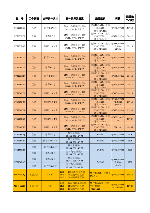
20*12
FT5402DQT
互容
推荐7-10.1寸
27*16
FT5206GE1
互容
推荐2.8-5寸
Sito:金属架桥,OGS Dito:G+G,G+F+F Sito:金属架桥,OGS Dito:G+G,G+F+F Sito:金属架桥,OGS Dito:G+G,G+F+F Sito:金属架桥,OGS Dito:G+G,G+F+F Sito:金属架桥,OGS Dito:G+G,G+F+F Sito:金属架桥,OGS Dito:G+G,G+F+F Sito:金属架桥,OGS Dito:G+G,G+F+F Sito:金属架桥,OGS Dito:G+G,G+F+F Sito:金属架桥,OGS Dito:G+G,G+F+F 横三角图案: GF,GG,OGS,GP,PF 横三角图案: GF,GG,OGS,GP,PF 横三角图案: GF,GG,OGS,GP,PF 竖三角2点图案: GF,GG,OGS,GP,PF 横三角图案: GF,GG,OGS,GP,PF 竖三角2点图案: GF,GG,OGS,GP,PF G1M – OGS结构单层互容 GFM – GF结构单层互容 GGM – GG结构单层互容 G1M – OGS 结构单层互容 GFM – GF结构单层互容 GGM – GG结构单层互容
工作电流:6mA 待机电流:4mA 睡眠电流:30uA
工作温度: -20~+85 储存温度: -55~+150 工作温度: -20~+85 储存温度: -55~+150
CY7C1411AV18资料

Errata Revision: *CMay 02, 2007RAM9 QDR-I/DDR-I/QDR-II/DDR- II ErrataCY7C129*DV18/CY7C130*DV25CY7C130*BV18/CY7C130*BV25/CY7C132*BV25CY7C131*BV18 / CY7C132*BV18/CY7C139*BV18CY7C191*BV18/CY7C141*AV18 / CY7C142*AV18/CY7C151*V18 /CY7C152*V18This document describes the DOFF issue for QDRII/DDRII and the Output Buffer and JTAG issues for QDRI/DDRI/QDRII/DDRII. Details include trigger conditions, possible workarounds and silicon revision applicability.This document should be used to compare to the respective datasheet for the devices to fully describe the device functionality.Please contact your local Cypress Sales Representative for availability of the fixed devices and any other questions.Devices AffectedTable 1. List of Affected devicesProduct StatusAll of the above densities and revisions are available in sample as well as production quantities.QDR/DDR DOFF Pin, Output Buffer and JTAG Issues Errata SummaryThe following table defines the issues and the fix status for the different devices which are affected.Density & Revision Part Numbers Architecture 9Mb - Ram9(90 nm)CY7C130*DV25QDRI/DDRI 9Mb - Ram9(90 nm)CY7C129*DV18QDRII 18Mb - Ram9(90nm)CY7C130*BV18CY7C130*BV25CY7C132*BV25QDRI/DDRI18Mb - Ram9(90nm)CY7C131*BV18CY7C132*BV18CY7C139*BV18CY7C191*BV18QDRII/DDRII36Mb - Ram9(90nm)CY7C141*AV18CY7C142*AV18QDRII/DDRII 72Mb -Ram9(90nm)CY7C151*V18CY7C152*V18QDRII/DDRIIItemIssueDeviceFix Status1.DOFF pin is used for enabling/dis-abling the DLL circuitry within the SRAM. To enable the DLL circuitry, DOFF pin must be externally tied HIGH. The QDR-II/DDR-II devices have an internal pull down resistor of ~5K . The value of the external pull-up resistor should be 500 or less in order to ensure DLL is enabled.9Mb - “D” Rev - Ram918Mb - “B” Rev - Ram936Mb - “A” Rev - Ram972Mb - Ram9QDR-II/DDR-II DevicesThe fix involved removing the in-ternal pull-down resistor on the DOFF pin. The fix has been im-plemented on the new revision and is now available.ΩΩTable 2.Issue Definition and fix status for different devices1. DOFF Pin Issue•ISSUE DEFINITIONThis issue involves the DLL not turning ON properly if a large resistor is used (eg:-10K ) as an external pullup resistor to enable the DLL. If a 10K or higher pullup resistor is used externally, the voltage on DOFF is not high enough to enable the DLL.•PARAMETERS AFFECTEDThe functionality of the device will be affected because of the DLL is not turning ON properly. When the DLL is enabled, all AC and DC parameters on the datasheet are met. •TRIGGER CONDITION(S)Having a 10K or higher external pullup resistor for disabling the DOFF pin.•SCOPE OF IMPACTThis issue will alter the normal functionality of the QDRII/DDRII devices when the DLL is disabled.•EXPLANATION OF ISSUEFigure 1 shows the DOFF pin circuit with an internal 5K internal resistor. The fix planned is to disable the internal 5K leaker.•WORKAROUND2.O/P Buffer enters a locked up unde-fined state after controls or clocks are left floating. No proper read/write access can be done on the device until a dummy read is performed.9Mb - “D” Rev - Ram918Mb - “B” Rev - Ram936Mb - “A” Rev - Ram972Mb - Ram9QDR-I/DDR-I/QDR-II/DDR-II Devices The fix has been implemented onthe new revision and is now avail-able.3.The EXTEST function in the JTAG test fails when input K clock is floating in the JTAG mode.9Mb - “D” Rev - Ram918Mb - “B” Rev - Ram936Mb - “A” Rev - Ram972Mb - Ram9QDR-I/DDR-I/QDR-II/DDR-II DevicesThe fix involved bypassing the ZQ circuitry in JTAG mode. This was done by overriding the ZQ circuit-ry by the JTAG signal. The fix has been implemented on the new re-vision and is now available.Figure 1.DOFF pin with the 5K internal resistorItemIssueDeviceFix StatusΩΩΩΩΩΩThe workaround is to have a low value of external pullup resistor for the DOFF pin (recommended value is <500). When DOFF pins from multiple QDR devices are connected through the same pull-up resistors on the board, it is recommended that this DOFF pin be directly connected to Vdd due to the lower effective resistance since the "leakers" are in parallel.Figure 2 shows the proposed workaround and the fix planned.•FIXSTATUSFix involved removing the internal pull-down resistor on the DOFF pin. The fix has been implemented on the new revision and is now available. The new revision is an increment of the existing revision. The following table lists the devices affected, current revision and the new revision after the fix.Table 3.List of Affected Devices and the new revison2.Output Buffer IssueFigure 2.Proposed workaround with the 500 external pullupCurrent Revision New Revision after the FixCY7C129*DV18CY7C129*EV18CY7C131*BV18CY7C131*CV18CY7C132*BV18CY7C132*CV18CY7C139*BV18CY7C139*CV18CY7C191*BV18CY7C191*CV18CY7C141*AV18CY7C141*BV18CY7C142*AV18CY7C142*BV18CY7C151*V18CY7C151*AV18CY7C152*V18CY7C152*AV18ΩΩ•ISSUE DEFINITIONThis issue involves the output buffer entering an unidentified state when the input signals (only Control signals or Clocks) are floating during reset or initialization of the memory controller after power up. •PARAMETERS AFFECTEDNo timing parameters are affected. The device may drive the outputs even though the read operation is not enabled. A dummy read is performed to clear this condition.•TRIGGER CONDITION(S)Input signals(namely RPS# for QDR-I/QDRII , WE# and LD# for DDR-I/DDRII) or Clocks (K/K# and/or C/C#) are floating during reset or initialization of the memory controller after power up.•SCOPE OF IMPACTThis issue will jeopardize any number of writes or reads which take place after the controls or clock are left floating. This can occur anywhere in the SRAM access ( all the way from power up of the memory device to transitions taking place for read/write accesses to the memory device) if the above trigger conditions are met.•EXPLANATION OF ISSUEFigure 3 shows the output register Reset circuit with an SR Latch circled. This latch has two inputs with one of them coming from some logic affected by the clock and RPS#(QDR) or WE# and LD#(DDR).The issue happens when clocks are glitching/toggling with controls floating. This will cause the SR latch to be taken into an unidentified state. The SR Latch will need to be reset by a dummy read operation if this happens. Array•WORKAROUNDThis is viable only if the customer has the trigger conditions met during reset or initialization of the memory controller after power up. In order for the workaround to perform properly, Cypress recommends the insertion of a minimum of 16 “dummy” READ operations to every SRAM device on the board prior to writing any meaningful data into the SRAM. After this one “dummy” READ operation, the device will perform properly.“Dummy” READ is defined as a read operation to the device that is not meant to retrieve required data. The “dummy” READ can be to any address location in the SRAM. Refer to Figure 4 for the dummy read implemen-tation.In systems where multiple SRAMs with multiple RPS# lines are used, a dummy read operation will have to be performed on every SRAM on the board. Below is an example sequence of events that can be performed before valid access can be performed on the SRAM.1) Initialize the Memory Controller2) Assert RPS# Low for each of the memory devicesNote:For all devices with x9 bus configuration, the following sequence needs to be performed:1) For the 72M / 36M / 18M x9 devices drive address pin A2 / A10 / A3 low respectively and perform dummyread.2) For the 72M / 36M / 18M x9 devices drive address pin A2 / A10 / A3 high respectively and perform dummyread.If the customer has the trigger conditions met during normal access to the memory then there is no workaround at this point.•FIX STATUSThe fix has been implemented on the new revision and is now available. The new revision is an increment of the existing revision. Please refer to Table 4 for the list of devices affected, current revision and the new revision after the fix.3. JTAG Mode Issue•ISSUE DEFINITIONIf the input clock (K Clock) is left floating when the device is in JTAG mode, spurious high frequency noise on this input can be interpreted by the device as valid clocks. This could cause the impedance matching circuitry (ZQ) on the QDR/DDR devices to periodically load itself with incorrect values. These incorrect values in the ZQ register could force the outputs into a High-Impedance state. The ZQ circuitry requires at least 1000 valid K clock cycles to drive the outputs from high impedance to low impedance levels.•PARAMETERS AFFECTEDThis issue only affects the EXTEST command when the device is in the JTAG mode. The normal functionality of the device will not be affected.•TRIGGER CONDITION(S)EXTEST command executed immediately after power-up without providing any K clock cycles.•SCOPE OF IMPACTThis issue only impacts the EXTEST command when device is tested in the JTAG mode. Normal functionality of the device is not affected. •EXPLANATION OF ISSUEImpedance matching circuitry (ZQ) is present on the QDR/DDR devices to set the desired impedance on the outputs. This ZQ circuitry is updated every 1000 clock cycles of K clock to ensure that the impedance of the O/P is set to valid state. However, when the device is operated in the JTAG mode immediately after power-up, high frequency noise on the input K clock can be treated by the ZQ circuitry as valid clocks thereby setting the outputs in to a high-impedance mode. If a minimum of 1000 valid K clocks are applied before performing the JTAG test, this should clear the ZQ circuitry and ensure that the outputs are driven to valid impedance levels.•WORKAROUNDElimination of the issue: After power-up, before any valid operations are performed on the device, insert a minimum of 1000 valid clocks on K input.•FIX STATUSThe fix involved bypassing the ZQ circuitry in JTAG mode. This was done by overriding the ZQ circuitry by the JTAG signal. The fix has been implemented on the new revision and is now available. The new revision is an increment of the existing revision. Please refer to Table 4 for the list of devices affected, current revision and the new revision after the fix..Table 4.List of Affected devices and the new revisionCurrent Revision New Revision after the FixCY7C129*DV18CY7C129*EV18CY7C130*DV25CY7C130*EV25CY7C130*BV18CY7C130*CV18CY7C130*BV25CY7C130*CV25CY7C132*BV25CY7C132*CV25CY7C131*BV18CY7C131*CV18CY7C132*BV18CY7C132*CV18CY7C139*BV18CY7C139*CV18CY7C191*BV18CY7C191*CV18CY7C141*AV18CY7C141*BV18CY7C142*AV18CY7C142*BV18CY7C151*V18CY7C151*AV18CY7C152*V18CY7C152*AV18ReferencesAll 90nm QDRI/DDRI/QDRII/DDRII datasheets:-Table 5.List of Datasheet spec# for the Affected devicesSpec#Part#DensityArchitecture38-05628CY7C1304DV259-MBIT QDR(TM) SRAM 4-WORD BURST 38-05632CY7C1308DV259-MBIT DDR-I SRAM 4-WORD BURST 001-00350CY7C1292DV18/1294DV189-MBIT QDR- II(TM) SRAM 2-WORD BURST 38-05621CY7C1316BV18/1916BV18/1318BV18/1320BV1818-MBIT DDR-II SRAM 2-WORD BURST 38-05622CY7C1317BV18/1917BV18/1319BV18/1321BV1818-MBIT DDR-II SRAM 4-WORD BURST 38-05623CY7C1392BV18/1393BV18/1394BV1818-MBIT DDR-II SIO SRAM 2-WORD BURST 38-05631CY7C1323BV2518-MBIT DDR-I SRAM 4-WORD BURST 38-05630CY7C1305BV25/1307BV2518-MBIT QDR(TM) SRAM 4-WORD BURST 38-05627CY7C1303BV25/1306BV2518-MBIT QDR(TM) SRAM 2-WORD BURST 38-05629CY7C1305BV18/1307BV1818-MBIT QDR(TM) SRAM 4-WORD BURST 38-05626CY7C1303BV18/1306BV1818-MBIT QDR(TM) SRAM 2-WORD BURST 38-05619CY7C1310BV18/1910BV18/1312BV18/1314BV1818-MBIT QDR - II (TM) SRAM 2-WORD BURST 38-05620CY7C1311BV18/1911BV18/1313BV18/1315BV1818-MBIT QDR - II SRAM 4-WORD BURST 38-05615CY7C1410AV18/1425AV18/1412AV18/1414AV1836-MBIT QDR-II(TM) SRAM 2-WORD BURST 38-05614CY7C1411AV18/1426AV18/1413AV18/1415AV1836-MBIT QDR(TM)-II SRAM 4-WORD BURST 38-05616CY7C1416AV18/1427AV18/1418AV18/1420AV1836-MBIT DDR-II SRAM 2-WORD BURST 38-05618CY7C1417AV18/1428AV18/1419AV18/1421AV1836-MBIT DDR-II SRAM 4-WORD BURST 38-05617CY7C1422AV18/1429AV18/1423AV18/1424AV1836-MBIT DDR-II SIO SRAM 2-WORD BURST 38-05489CY7C1510V18/1525V18/1512V18/1514V1872-MBIT QDR-II SRAM 2-WORD BURST 38-05363CY7C1511V18/1526V18/1513V18/1515V1872-MBIT QDR(TM)-II SRAM 4-WORD BURST 38-05563CY7C1516V18/1527V18/1518V18/1520V1872-MBIT DDR-II SRAM 2-WORD BURST 38-05565CY7C1517V18/1528V18/1519V18/1521V1872-MBIT DDR-II SRAM 4-WORD BURST 38-05564CY7C1522V18/1529V18/1523V18/1524V1872-MBITDDR-II SIO SRAM 2-WORD BURSTDocument History PageDocument Title: RAM9 QDR-I/DDR-I/QDR-II/DDR- II Errata Document #: 001-06217 Rev. *CREV.ECN NO.IssueDateOrig. ofChange Description of Change**419849See ECN REF New errata for Ram9 QDR2/DDR2 SRAMs.*A493936See ECN QKS Added Output buffer and JTAG mode issues, Item#2 and #3Added 9Mb QDR-II Burst of 2 and QDR-1/DDR-I part numbers.*B733176See ECN NJY Added missing part numbers in the title for Spec#’s 38-05615,38-05614,38-05363,38-05563 on Table 5 on page 7.*C1030020 See ECN TBE Updated the fix status of the three issues, and modified the description forthe Output Buffer workaround for x9 devices on page 5.。
AIC1723A-18CETR中文资料
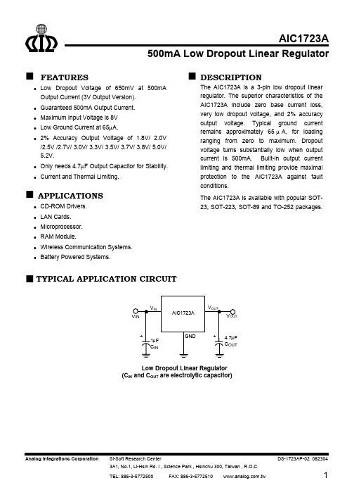
500mA Low Dropout Linear RegulatorFEATURESLow Dropout Voltage of 650mV at 500mA Output Current (3V Output Version). Guaranteed 500mA Output Current. Maximum Input Voltage is 8V Low Ground Current at 65µA.2% Accuracy Output Voltage of 1.8V/ 2.0V/2.5V /2.7V/ 3.0V/ 3.3V/ 3.5V/ 3.7V/ 3.8V/ 5.0V/ 5.2V.Only needs 4.7µF Output Capacitor for Stability.Current and Thermal Limiting.APPLICATIONSCD-ROM Drivers. LAN Cards. Microprocessor. RAM Module.Wireless Communication Systems.Battery Powered Systems.DESCRIPTIONThe AIC1723A is a 3-pin low dropout linearregulator. The superior characteristics of the AIC1723A include zero base current loss, very low dropout voltage, and 2% accuracy output voltage. Typical ground current remains approximately 65µA, for loading ranging from zero to maximum. Dropout voltage turns substantially low when output current is 500mA. Built-in output current limiting and thermal limiting provide maximal protection to the AIC1723A against fault conditions.The AIC1723A is available with popular SOT-23, SOT-223, SOT-89 and TO-252 packages.TYPICAL APPLICATION CIRCUITLow Dropout Linear Regulator(C IN and C OUT are electrolytic capacitor)Packing TypeAIC1723A-18PYTR1.8V Version, in SOT-223 Lead Free Package & Tape& Reel Packing TypeSOT-23 MARKINGPart No. CU PU Part No. CU PU AIC1723A-18XU BT18 BT18P AIC1723A-35XU BT35 BT35P AIC1723A-20XU BT20 BT20P AIC1723A-37XU BT37 BT37P AIC1723A-25XU BT25 BT25P AIC1723A-38XU BT38 BT38P AIC1723A-27XU BT27 BT27P AIC1723A-50XU BT50 BT50P AIC1723A-30XU BT30 BT30P AIC1723A-52XU BT52 BT52P AIC1723A-33XU BT33 BT33PSOT-89 MARKINGPart No. CX PX Part No. CX PXAIC1723A-18XX AV18 AV18P AIC1723A-35XX AV35 AV35PAIC1723A-20XX AV20 AV20P AIC1723A-37XX AV37 AV37PAIC1723A-25XX AV25 AV25P AIC1723A-38XX AV38 AV38PAIC1723A-27XX AV27 AV27P AIC1723A-50XX AV50 AV50PAIC1723A-30XX AV30 AV30P AIC1723A-52XX AV52 AV52PAIC1723A-33CY AV33 AV33PSOT-223 MARKINGPart No. CY PY Part No. CY PYAIC1723A-18XY BU18 BU18P AIC1723A-35XY BU35 BU35PAIC1723A-20XY BU20 BU20P AIC1723A-37XY BU37 BU37PAIC1723A-25XY BU25 BU25P AIC1723A-38XY BU38 BU38PAIC1723A-27XY BU27 BU27P AIC1723A-50XY BU50 BU50PAIC1723A-30XY BU30 BU30P AIC1723A-52XY BU52 BU52PAIC1723A-33XY BU33 BU33PABSOLUTE MAXIMUM RATINGSInput Supply Voltage ...................................................…………..…….................. -0.3~8VOperating Temperature Range …………….....………........…………................-40°C~ 85°CJunction Temperature ……………………………………………………………………... 125°CStorage Temperature Range ....................……......................………............. -65°C~150°CLead Temperature (Soldering. 10sec) …………………………………………………… 260°CThermal Resistance Junction to Ambient SOT-23 Package ...….………..… 180°C/W(Assume no Ambient Airflow, no Heatsink) TO-252 Package ...….………..… 100°C/W...….………..… 160°C/W SOT-89PackagePackage...….………..… 155°C/W SOT-223Absolute Maximum Rating are those value beyond which the life of a device may be impaired.TEST CIRCUITRefer to the TYPICAL APPLICATION CIRCUITELECTRICAL CHARACTERISTICS (T A =25°C, C IN =1µF, C OUT =4.7µF, unlessotherwise specified.) (Note 1)PARAMETERTEST CONDITIONSMIN.TYP.MAX. UNITNo LoadOutput Voltage AIC1723A-52 AIC1723A-50 AIC1723A-38 AIC1723A-37 AIC1723A-35 AIC1723A-33 AIC1723A-30AIC1723A-27 AIC1723A-25 AIC1723A-20 AIC1723A-18V IN =8V-2+2 %Line Regulation I L =1mA, 1.8V ≤V OUT ≤3.2V 3.3V ≤V OUT ≤5.2V V IN =4V~8V V IN =5.5V~8V 3 310 15mV Load Regulation (Note 2) I L =0.1~500mA 1.8V ≤V OUT ≤3.9V4.0V ≤V OUT ≤5.2VV IN =5V V IN =7V 10 20 30 50 mV Current Limit(Note 3)V IN =7V, V OUT =0V 500 mADropout Voltage(Note 4)I L =500mA 4.0V ≤V OUT ≤5.2V3.0V ≤V OUT ≤3.9V 2.5V ≤V OUT ≤2.9V 2.0V ≤V OUT ≤2.4V 1.8V ≤V OUT ≤1.9V510 65078011001400 mV Ground Current I O =0.1mA~I MAX 1.8V ≤V OUT ≤3.9V 4.0V ≤V OUT ≤5.2V V IN =5~8V V IN =7~8V 65 659090µANote 1: Specifications are production tested at T A =25°C. Specifications over the -40°C to 85°C operating temperature range are assured by design, characterization and correlation with Statistical Quality Controls (SQC).Note 2:Regulation is measured at constant junction temperature, using pulse testing with a low ON time. Note 3: Current limit is measured by pulsing a short time.Note 4:Dropout voltage is defined as the input to output differential at which the output voltage drops 100mV below the value measured with a 1V differential.TYPICAL PERFORMANCE CHARACTERISTICS0 50100150200250300350400450V DROP vs. I LOADV D R O P (m V )I LOAD (mA)0V DROP vs. I LOADV D R O P (m V )I LOAD (mA)300320340360380400420440V DROP vs. TemperatureV D R O P (m V )Temperature (°C)-40-30-20-1001020304050607080-40-2020406080V DROP vs. TemperatureV D R O P (m V )Temperature (°C)0102030405060Ground Current vs. V ING r o u n d C u r r e n t (µA )V IN (V)Ground Current vs. V ING r o u n d C u r r e n t (µA )V IN (V)TYPICAL PERFORMANCE CHARACTERISTICS (Continued)Ground Current vs. TemperatureG r o u n d C u r r e n t (µA )Temperature (°C)Current Limit vs. TemperatureC u r r e n t L i m i t (m A )Temperature (°C)V OUT vs. TemperatureV O U T (V )Temperature (°C)V OUT vs. TemperatureV O U T (V )Temperature (°C)BLOCK DIAGRAMGNDVOUTVINPIN DESCRIPTIONSVOUT PIN - Output pin. GND PIN - Power GND. VIN PIN - Power Supply Input.PHYSICAL DIMENSIONS (unit: mm)SOT-23 (CU) (PU)SYMBOL MIN MAXA 0.95 1.45 A1 0.05 0.15 A2 0.90 1.30b 0.30 0.50c 0.08 0.22 D 2.80 3.00 E 2.60 3.00 E1 1.50 1.70 e 0.95 BSCe1 1.90 BSC L 0.30 0.60 L1 0.60 REFθ 0˚ 8˚TO-252 (CE) (PE)SYMBOL MIN MAXA 2.19 2.38A1 0.00 0.13b 0.64 0.89b3 5.21 5.46c 0.46 0.61c2 0.46 0.58D 5.33 6.22E 6.35 6.73e 2.28BSCH 9.40 10.41L 1.40 1.78 L1 2.67REF L2 0.51BSC L3 0.89 2.03L4 0.641.02θ0°8°SOT-89 (CX) (PX)SYMBOL MIN MAXA 1.40 1.60B 0.44 0.56B1 0.36 0.48C 0.35 0.44D 4.40 4.60D1 1.50 1.83E 2.29 2.60e 1.50BSCe1 3.00BSCH 3.94 4.25L 0.89 1.20SOT-223 (CY) (PY)SYMBOL MIN MAXA - 1.80A1 0.02 0.10A2 1.55 1.65b 0.66 0.84b2 2.90 3.10c 0.23 0.33D 6.30 6.70E 6.70 7.30E1 3.30 3.70e 2.30BSC e1 4.60BSC L 0.90 -θ0°8°Note:Information provided by AIC is believed to be accurate and reliable. However, we cannot assume responsibility for use of any circuitry other than circuitry entirely embodied in an AIC product; nor for any infringement of patents or other rights of third parties that may result from its use. We reserve the right to change the circuitry and specifications without notice.Life Support Policy: AIC does not authorize any AIC product for use in life support devices and/or systems. Life support devices or systems are devices or systems which, (I) are intended for surgical implant into the body or (ii) support or sustain life, and whose failure to perform, when properly used in accordance with instructions for use provided in the labeling, can be reasonably expected to result in a significant injury to the user.。
抗干扰检针机
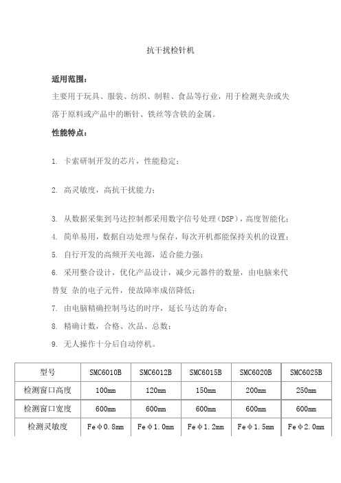
抗干扰检针机
适用范围:
主要用于玩具、服装、纺织、制鞋、食品等行业,用于检测夹杂或失落于原料或产品中的断针、铁丝等含铁的金属。
性能特点:
1. 卡索研制开发的芯片,性能稳定;
2. 高灵敏度,高抗干扰能力;
3. 从数据采集到马达控制都采用数字信号处理(DSP),高度智能化;
4. 简单易用,数据自动处理与保存,每次开机都能保持关机的设置;
5. 自行开发的高频开关电源,适合能力强;
6. 采用整合设计,优化产品设计,减少元器件的数量,由电脑来代替复杂的电子元件,使故障率成倍降低;
7. 由电脑精确控制马达的时序,延长马达的寿命;
8. 精确计数,合格、次品、总数;
9. 无人操作十分后自动停机。
相关参数:
输送速度:0.25-0.5m/s.
灵敏度:φ0.8mm-2.0㎜铁球。
电源: 220V 50Hz。
功率: 100W 。
报警方式:声光报警,并自动停机。
外型尺寸(长×宽×高㎜): 1850×1050×900 。
重量: 175㎏。
看到这里相信大家对检针机有了一定的了解,如果想要获得更多关于检针机的信息,请关注我们卡索电子!。
LT1763-1.5资料

U APPLICATIO S
s s s
Cellular Phones Battery-Powered Systems Noise-Sensitive Instrumentation Systems
The LT ®1763 series are micropower, low noise, low dropout regulators. The devices are capable of supplying 500mA of output current with a dropout voltage of 300mV. Designed for use in battery-powered systems, the low 30µA quiescent current makes them an ideal choice. Quiescent current is well controlled; it does not rise in dropout as it does with many other regulators. A key feature of the LT1763 regulators is low output noise. With the addition of an external 0.01µF bypass capacitor, output noise drops to 20µVRMS over a 10Hz to 100kHz bandwidth. The LT1763 regulators are stable with output capacitors as low as 3.3µF. Small ceramic capacitors can be used without the series resistance required by other regulators. Internal protection circuitry includes reverse battery protection, current limiting, thermal limiting and reverse current protection. The parts come in fixed output voltages of 1.5V, 1.8V, 2.5V, 3V, 3.3V and 5V, and as an adjustable device with a 1.22V reference voltage. The LT1763 regulators are available in the 8-lead SO package.
集成电路英文代码对照

集成电路英文代码及中文对照(一)我的文摘2009-11-21 11:32:53 阅读111 评论0 字号:大中小订阅产品名称型号规格性能说明LMLM24J 四运放(军用级)LM148J 通用四运放LM1875T 无线电控制/接收器LM224J 四运放(工业级)LM258N 分离式双电源双运放LM2901N 四电压比较器LM2904N 四运放LM301AN 通用运算放大器LM308N 单比较器LM311P 单比较器LM317L 可调三端稳压器/100mALM317T 可调三端稳压器/1.5ALM317K 可调三端稳压器/3ALM318 高速宽带运放LM324K 通用四运放LM331N V-F/F-V转换器LM336-2.5V 基准电压电路LM336 5V 基准电压电路LM337T 基准电压电路1ALM338K 可调三端稳压器5ALM339N 四比较器LM348N 四741运放LM358N 低功耗双运放LM361N 高速差动比较器LM386N 声频功率放大器LM3914N 十段点线显示驱动LM393N 低功耗低失调双比较器LM399H 精密基准源(6.9)LM723CN 可调正式负稳压器LM733CN 视频放大器LM741J 单运放LM741CN 双运放NENE521 高速双差分比较器NE5532 双运放NE5534 双运放NE555N 单运放NE555J 时基电路军品极NE556 双级型双时基电路NE564 锁相环NE565 锁相环NE567 音调译码器NE592 视频放大器OPOP07 低噪声运放OP27 超低噪声精密运放OP37 超低噪声精密运放光电耦合4N25 晶体管输出4N25MC 晶体管输出4N26 晶体管输出4N27 晶体管输出4N28 晶体管输出4N29 达林顿输出4N30 达林顿输出4N31 达林顿输出4N32 达林顿输出4N33 达林顿输出4N33MC 达林顿输出4N35 达林顿输出4N36 晶体管输出4N37 晶体管输出4N38 晶体管输出4N39 可控硅输出6N135 高速光耦晶体管输出6N136 高速光耦晶体管输出6N137 高速光耦晶体管输出6N138 达林顿输出6N139 达林顿输出MOC3020 可控硅驱动输出MOC3021 可控硅驱动输出MOC3023 可控硅驱动输出MOC3030 可控硅驱动输出MOC3040 过零触发可控硅输出MOC3041 过零触发可控硅输出MOC3061 过零触发可控硅输出MOC3081 过零触发可控硅输出TLP521-1 单光耦TLP521-2 双光耦TLP521-4 四光耦TLP621 四光耦TIL113 达林顿输出TIL117 TLL逻辑输出PC814 单光耦PC817 单光耦H11A2 晶体管输出H11D1 高压晶体管输出H11G2 电阻达林顿输出LFLF347N 宽带JFET输入四运放LF351N 宽带JFET输入运放LF353N JFET输入宽带运放LF355N JFET输入运放LF357N JFET宽带非全裣运放LF398N 采样/保持电路LF412N 低偏差飘移输入运放MCMC1377 彩色电视编码器MC1403 精密电压基准源(2.5)MC1413 周边七段驱动阵列MC1416 周边七段驱动陈列MC14409 二进制脉冲拨号器MC14433 3位半A/D转换器MC14489 多字符LED显示驱动器MC145026 编码器VD5026 编码器MC145027 译码器VD5027 译码器MC145028 译码器MC145030 编码译码器MC145106 频率合成器MC145146 4位数据总线TLTL062 低功耗JEFT输入双运放TL072 低噪声JEFTTL082TL084TL431TL494ULNULN2003 周边七段驱动陈列ULN2004 周边七段驱动陈列ULN2803 周边八段驱动陈列ULN2804 周边八段驱动陈列ICLICL7106 3位ADC/驱动LCDICL7107 3位半ADC/驱动LEDICL7109 4位半ADC/驱动LEDICL7129 4位半ADC/LCD驱动ICL7135 ADC/LCD驱动BCD输出ICL7136 3位半CMOSADC/LCD驱动ICL7218 CMOS低功耗运算放大器ICL7650 整零运放斩波ICL7652 整零运放斩波ICL7660 CMOS直流-直流转换器ICL8038 函数信号发生器ICL8049 反对数放大器CACA3140 单BIMOS运行CA3240 单BIMOS运行UCUC3842 WM电流型控制器UC3845 PWM电流型控制器DSDS12887 非易失实时时钟芯片L3845 中继接口电路SGSG3524 PWM解调调制器SG3525 PWM解调调制器20106 前置放大器MTMT8814 8x12模拟交换矩阵MT8816 8x模拟交换矩阵MT8870 综合DTMF接收器MT8870 综合DTMF接收器MT8880 综合DTMF发生接收器MIC24LC01 128x8串行EEPROM24LC02 256x8串行EEPROM24LC04 512x8串行EEPROM24LC16 2Kx8串行EEPROM93LC46 64x16串行EEPROM93LC56 256x16串行EEPROM93LC66 512x8 256x16 EEPROMPIC16C52 384x12 单片机PIC16C54 512x12 单片机PCI16C56 512x12 单片机PIC16C57 2048x12 单片机ATAT24C01 128x8串行EEPROMAT24C02 256x8串行EEPROMAT24C04 512x8串行EEPROMAT24C16 2Kx8串行EEPROMAT93C46 64x16串行EEPROMAT93C56 256x16串行EEPROMATF16V8 FLASH200门ATF20V8 FLASH300门高速ATF22V10 FLASH500门高速低电流AT28C16 2Kx8CMOS并行EEPROMAT28C17 2Kx8CMOS并行EEPROMAT28C64 8Kx8并行EEPROMAT28C256 32Kx8并行EEPROMAT28F010 128Kx8并行EEPROMA29C040 512Kx8 FLASH EEPROMHM6116 2Kx8 CMOS 静态PAMHY6264 8Kx8 CMOS 静态RAMHM6264 8Kx8 CMOS 静态RAMIS62C64 8Kx8 高速CMOS 静态RAMHY62256 32Kx8 CMOS 静态RAMHM62256 32Kx8 CMOS 静态RAMHM628128 128Kx8 CMOS 静态RAMHM628256 256Kx8 CMOS 静态RAMHM628512 512Kx8 CMOS 静态RAMHM628512 512Kx8 CMOS 静态RAM TCMTCM5087 双音调发生器MM5832 实时钟电路TCTC14433 3位半A/D转换器TC232 并行/串行接口电路TC7106 3位半ADC/LCD驱动TC7107 3位半ADC/LED驱动TC7116 3位半ADC/LCD驱动带保TC7129 4位半ADC/LCDTC7135 4位半ADC/LCD,BCD输出TC7650 整零运放斩波7575107 四差分线驱动器75174 四差分线驱动器75175 三态四差分接收器75176 差分总线接收器75188 四线驱动器75189 四线驱动器75451 双外围驱动器75452 双外围驱动器集成电路英文代码及中文对照(二)我的文摘2009-11-21 11:37:11 阅读191 评论0 字号:大中小订阅。
常用开关电源芯片大全之欧阳育创编

常用开关电源芯片大全第1章DC-DC电源转换器/基准电压源1.1 DC-DC电源转换器1.低噪声电荷泵DC-DC电源转换器AAT3113/AAT31142.低功耗开关型DC-DC电源转换器ADP30003.高效3A开关稳压器AP15014.高效率无电感DC-DC电源转换器FAN56605.小功率极性反转电源转换器ICL76606.高效率DC-DC电源转换控制器IRU30377.高性能降压式DC-DC电源转换器ISL64208.单片降压式开关稳压器L49609.大功率开关稳压器L4970A10.1.5A降压式开关稳压器L497111.2A高效率单片开关稳压器L497812.1A高效率升压/降压式DC-DC电源转换器L597013.1.5A降压式DC-DC电源转换器LM157214.高效率1A降压单片开关稳压器LM1575/LM2575/LM2575HV15.3A降压单片开关稳压器LM2576/LM2576HV16.可调升压开关稳压器LM257717.3A降压开关稳压器LM259618.高效率5A开关稳压器LM267819.升压式DC-DC电源转换器LM2703/LM270420.电流模式升压式电源转换器LM273321.低噪声升压式电源转换器LM275022.小型75V降压式稳压器LM500723.低功耗升/降压式DC-DC电源转换器LT107324.升压式DC-DC电源转换器LT161525.隔离式开关稳压器LT172526.低功耗升压电荷泵LT175127.大电流高频降压式DC-DC电源转换器LT176528.大电流升压转换器LT193529.高效升压式电荷泵LT193730.高压输入降压式电源转换器LT195631.1.5A升压式电源转换器LT196132.高压升/降压式电源转换器LT343333.单片3A升压式DC-DC电源转换器LT343634.通用升压式DC-DC电源转换器LT346035.高效率低功耗升压式电源转换器LT346436.1.1A升压式DC-DC电源转换器LT346737.大电流高效率升压式DC-DC电源转换器LT378238.微型低功耗电源转换器LTC175439.1.5A单片同步降压式稳压器LTC187540.低噪声高效率降压式电荷泵LTC191141.低噪声电荷泵LTC3200/LTC3200-542.无电感的降压式DC-DC电源转换器LTC325143.双输出/低噪声/降压式电荷泵LTC325244.同步整流/升压式DC-DC电源转换器LTC340145.低功耗同步整流升压式DC-DC电源转换器LTC340246.同步整流降压式DC-DC电源转换器LTC340547.双路同步降压式DC-DC电源转换器LTC340748.高效率同步降压式DC-DC电源转换器LTC341649.微型2A升压式DC-DC电源转换器LTC342650.2A两相电流升压式DC-DC电源转换器LTC342851.单电感升/降压式DC-DC电源转换器LTC344052.大电流升/降压式DC-DC电源转换器LTC344253.1.4A同步升压式DC-DC电源转换器LTC345854.直流同步降压式DC-DC电源转换器LTC370355.双输出降压式同步DC-DC电源转换控制器LTC373656.降压式同步DC-DC电源转换控制器LTC377057.双2相DC-DC电源同步控制器LTC380258.高性能升压式DC-DC电源转换器MAX1513/MAX151459.精简型升压式DC-DC电源转换器MAX1522/MAX1523/MAX152460.高效率40V升压式DC-DC电源转换器MAX1553/MAX155461.高效率升压式LED电压调节器MAX1561/MAX159962.高效率5路输出DC-DC电源转换器MAX156563.双输出升压式DC-DC电源转换器MAX1582/MAX1582Y64.驱动白光LED的升压式DC-DC电源转换器MAX158365.高效率升压式DC-DC电源转换器MAX1642/MAX164366.2A降压式开关稳压器MAX164467.高效率升压式DC-DC电源转换器MAX1674/MAX1675/MAX167668.高效率双输出DC-DC电源转换器MAX167769.低噪声1A降压式DC-DC电源转换器MAX1684/MAX168570.高效率升压式DC-DC电源转换器MAX169871.高效率双输出降压式DC-DC电源转换器MAX171572.小体积升压式DC-DC电源转换器MAX1722/MAX1723/MAX172473.输出电流为50mA的降压式电荷泵MAX173074.升/降压式电荷泵MAX175975.高效率多路输出DC-DC电源转换器MAX180076.3A同步整流降压式稳压型MAX1830/MAX183177.双输出开关式LCD电源控制器MAX187878.电流模式升压式DC-DC电源转换器MAX189679.具有复位功能的升压式DC-DC电源转换器MAX194780.高效率PWM降压式稳压器MAX1992/MAX199381.大电流输出升压式DC-DC电源转换器MAX61882.低功耗升压或降压式DC-DC电源转换器MAX62983.PWM升压式DC-DC电源转换器MAX668/MAX66984.大电流PWM降压式开关稳压器MAX724/MAX72685.高效率升压式DC-DC电源转换器MAX756/MAX75786.高效率大电流DC-DC电源转换器MAX761/MAX76287.隔离式DC-DC电源转换器MAX8515/MAX8515A88.高性能24V升压式DC-DC电源转换器MAX872789.升/降压式DC-DC电源转换器MC33063A/MC34063A90.5A升压/降压/反向DC-DC电源转换器MC33167/MC3416791.低噪声无电感电荷泵MCP1252/MCP125392.高频脉宽调制降压稳压器MIC220393.大功率DC-DC升压电源转换器MIC229594.单片微型高压开关稳压器NCP1030/NCP103195.低功耗升压式DC-DC电源转换器NCP1400A96.高压DC-DC电源转换器NCP140397.单片微功率高频升压式DC-DC电源转换器NCP141098.同步整流PFM步进式DC-DC电源转换器NCP142199.高效率大电流开关电压调整器NCP1442/NCP1443/NCP1444/NCP1445100.新型双模式开关稳压器NCP1501101.高效率大电流输出DC-DC电源转换器NCP1550102.同步降压式DC-DC电源转换器NCP1570103.高效率升压式DC-DC电源转换器NCP5008/NCP5009 104.大电流高速稳压器RT9173/RT9173A105.高效率升压式DC-DC电源转换器RT9262/RT9262A106.升压式DC-DC电源转换器SP6644/SP6645107.低功耗升压式DC-DC电源转换器SP6691108.新型高效率DC-DC电源转换器TPS54350109.无电感降压式电荷泵TPS6050x110.高效率升压式电源转换器TPS6101x111.28V恒流白色LED驱动器TPS61042112.具有LDO输出的升压式DC-DC电源转换器TPS6112x 113.低噪声同步降压式DC-DC电源转换器TPS6200x114.三路高效率大功率DC-DC电源转换器TPS75003115.高效率DC-DC电源转换器UCC39421/UCC39422116.PWM控制升压式DC-DC电源转换器XC6371117.白光LED驱动专用DC-DC电源转换器XC9116118.500mA同步整流降压式DC-DC电源转换器XC9215/XC9216/XC9217119.稳压输出电荷泵XC9801/XC9802120.高效率升压式电源转换器ZXLB16001.2 线性/低压差稳压器121.具有可关断功能的多端稳压器BAXXX122.高压线性稳压器HIP5600123.多路输出稳压器KA7630/KA7631124.三端低压差稳压器LM2937125.可调输出低压差稳压器LM2991126.三端可调稳压器LM117/LM317127.低压降CMOS500mA线性稳压器LP38691/LP38693128.输入电压从12V到450V的可调线性稳压器LR8129.300mA非常低压降稳压器(VLDO)LTC3025130.大电流低压差线性稳压器LX8610131.200mA负输出低压差线性稳压器MAX1735132.150mA低压差线性稳压器MAX8875133.带开关控制的低压差稳压器MC33375134.带有线性调节器的稳压器MC33998135.1.0A低压差固定及可调正稳压器NCP1117136.低静态电流低压差稳压器NCP562/NCP563137.具有使能控制功能的多端稳压器PQxx138.五端可调稳压器SI-3025B/SI-3157B139.400mA低压差线性稳压器SPX2975140.五端线性稳压器STR20xx141.五端线性稳压器STR90xx142.具有复位信号输出的双路输出稳压器TDA8133143.具有复位信号输出的双路输出稳压器TDA8138/TDA8138A144.带线性稳压器的升压式电源转换器TPS6110x145.低功耗50mA低压降线性稳压器TPS760xx146.高输入电压低压差线性稳压器XC6202147.高速低压差线性稳压器XC6204148.高速低压差线性稳压器XC6209F149.双路高速低压差线性稳压器XC64011.3 基准电压源150.新型XFET基准电压源ADR290/ADR291/ADR292/ADR293151.低功耗低压差大输出电流基准电压源MAX610x152.低功耗1.2V基准电压源MAX6120153.2.5V精密基准电压源MC1403154.2.5V/4.096V基准电压源MCP1525/MCP1541155.低功耗精密低压降基准电压源REF30xx/REF31xx156.精密基准电压源TL431/KA431/TLV431A第2章AC-DC转换器及控制器1.厚膜开关电源控制器DP104C2.厚膜开关电源控制器DP308P3.DPA-Switch系列高电压功率转换控制器DPA423/DPA424/DPA425/DPA4264.电流型开关电源控制器FA13842/FA13843/FA13844/FA138455.开关电源控制器FA5310/FA53116.PWM开关电源控制器FAN75567.绿色环保的PWM开关电源控制器FAN76018.FPS型开关电源控制器FS6M07652R9.开关电源功率转换器FS6Sxx10.降压型单片AC-DC转换器HV-2405E11.新型反激准谐振变换控制器ICE1QS0112.PWM电源功率转换器KA1M088013.开关电源功率转换器KA2S0680/KA2S088014.电流型开关电源控制器KA38xx15.FPS型开关电源功率转换器KA5H0165R16.FPS型开关电源功率转换器KA5Qxx17.FPS型开关电源功率转换器KA5Sxx18.电流型高速PWM控制器L499019.具有待机功能的PWM初级控制器L599120.低功耗离线式开关电源控制器L659021.LINK SWITCH TN系列电源功率转换器LNK304/LNK305/LNK30622.LINK SWITCH系列电源功率转换器LNK500/LNK501/LNK52023.离线式开关电源控制器M51995A24.PWM电源控制器M62281P/M62281FP25.高频率电流模式PWM控制器MAX5021/MAX502226.新型PWM开关电源控制器MC4460427.电流模式开关电源控制器MC4460528.低功耗开关电源控制器MC4460829.具有PFC功能的PWM电源控制器ML482430.液晶显示器背光灯电源控制器ML487631.离线式电流模式控制器NCP120032.电流模式脉宽调制控制器NCP120533.准谐振式PWM控制器NCP120734.低成本离线式开关电源控制电路NCP121535.低待机能耗开关电源PWM控制器NCP123036.STR系列自动电压切换控制开关STR8xxxx37.大功率厚膜开关电源功率转换器STR-F665438.大功率厚膜开关电源功率转换器STR-G865639.开关电源功率转换器STR-M6511/STR-M652940.离线式开关电源功率转换器STR-S5703/STR-S5707/STR-S570841.离线式开关电源功率转换器STR-S6401/STR-S6401F/STR-S6411/STR-S6411F 442.开关电源功率转换器STR-S651343.离线式开关电源功率转换器TC33369~TC3337444.高性能PFC与PWM组合控制集成电路TDA16846/TDA1684745.新型开关电源控制器TDA1685046.“绿色”电源控制器TEA150447.第二代“绿色”电源控制器TEA150748.新型低功耗“绿色”电源控制器TEA153349.开关电源控制器TL494/KA7500/MB375950.Tiny SwitchⅠ系列功率转换器TNY253、TNY254、TNY25551.Tiny SwitchⅡ系列功率转换器TNY264P~TNY268G52.TOP Switch(Ⅱ)系列离线式功率转换器TOP209~TOP22753.TOP Switch-FX系列功率转换器TOP232/TOP233/TOP23454.TOP Switch-GX系列功率转换器TOP242~TOP25055.开关电源控制器UCX84X56.离线式开关电源功率转换器VIPer12AS/VIPer12ADIP57.新一代高度集成离线式开关电源功率转换器VIPer53第3章功率因数校正控制/节能灯电源控制器1.电子镇流器专用驱动电路BL83012.零电压开关功率因数控制器FAN48223.功率因数校正控制器FAN75274.高电压型EL背光驱动器HV8265.EL场致发光背光驱动器IMP525/IMP5606.高电压型EL背光驱动器/反相器IMP8037.电子镇流器自振荡半桥驱动器IR21568.单片荧光灯镇流器IR21579.调光电子镇流器自振荡半桥驱动器IR215910.卤素灯电子变压器智能控制电路IR216111.具有功率因数校正电路的镇流器电路IR216612.单片荧光灯镇流器IR216713.自适应电子镇流器控制器IR252014.电子镇流器专用控制器KA754115.功率因数校正控制器L656116.过渡模式功率因数校正控制器L656217.集成背景光控制器MAX8709/MAX8709A18.功率因数校正控制器MC33262/MC3426219.固定频率电流模式功率因数校正控制器NCP165320.EL场致发光灯高压驱动器SP440321.功率因数校正控制器TDA4862/TDA486322.有源功率因数校正控制器UC385423.高频自振荡节能灯驱动器电路VK05CFL24.大功率高频自振荡节能灯驱动器电路VK06TL第4章充电控制器1.多功能锂电池线性充电控制器AAT36802.可编程快速电池充电控制器BQ20003.可进行充电速率补偿的锂电池充电管理器BQ20574.锂电池充电管理电路BQ2400x5.单片锂电池线性充电控制器BQ2401xB接口单节锂电池充电控制器BQ2402x7.2A同步开关模式锂电池充电控制器BQ241008.集成PWM开关控制器的快速充电管理器BQ29549.具有电池电量计量功能的充电控制器DS277010.锂电池充电控制器FAN7563/FAN756411.2A线性锂/锂聚合物电池充电控制器ISL629212.锂电池充电控制器LA5621M/LA5621V13.1.5A通用充电控制器LT157114.2A恒流/恒压电池充电控制器LT176915.线性锂电池充电控制器LTC173216.带热调节功能的1A线性锂电池充电控制器LTC173317.线性锂电池充电控制器LTC173418.新型开关电源充电控制器LTC198019.开关模式锂电池充电控制器LTC400220.4A锂电池充电器LTC400621.多用途恒压/恒流充电控制器LTC400822.4.2V锂离子/锂聚合物电池充电控制器LTC405223.可由USB端口供电的锂电池充电控制器LTC405324.小型150mA锂电池充电控制器LTC405425.线性锂电池充电控制器LTC405826.单节锂电池线性充电控制器LTC405927.独立线性锂电池充电控制器LTC406128.镍镉/镍氢电池充电控制器M62256FP29.大电流锂/镍镉/镍氢电池充电控制器MAX150130.锂电池线性充电控制器MAX150731.双输入单节锂电池充电控制器MAX1551/MAX155532.单节锂电池充电控制器MAX167933.小体积锂电池充电控制器MAX1736B接口单节锂电池充电控制器MAX181135.多节锂电池充电控制器MAX187336.双路输入锂电池充电控制器MAX187437.单节锂电池线性充电控制器MAX189838.低成本/多种电池充电控制器MAX190839.开关模式单节锂电池充电控制器MAX1925/MAX192640.快速镍镉/镍氢充电控制器MAX2003A/MAX200341.可编程快速充电控制器MAX712/MAX71342.开关式锂电池充电控制器MAX74543.多功能低成本充电控制器MAX846A44.具有温度调节功能的单节锂电池充电控制器MAX8600/MAX860145.锂电池充电控制器MCP73826/MCP73827/MCP7382846.高精度恒压/恒流充电器控制器MCP73841/MCP73842/MCP73843/MCP73844 647.锂电池充电控制器MCP73861/MCP7386248.单节锂电池充电控制器MIC7905049.单节锂电池充电控制器NCP180050.高精度线性锂电池充电控制器VM7205。
线性恒流驱动ic型号大全
线性恒流驱动ic型号大全线性恒流驱动IC,就是恒流芯片led灯,所有电路,无非就是电阻,电容,电感,及一些二三极管组成的。
恒流主要是由恒流IC起到主要驱动作用,恒流的意思就是恒定电流,一般是在输入电压变化的情况下,输入电流保持不变。
而恒流驱动IC,只是一个集成电路,里面有恒流信号,使电路中的电压和电流在向量图上同相,互相之间即不超前,也不滞后。
1、高压线性恒流驱动IC-DT3100目前,高压线性恒流采用分段点亮的方式驱动高压灯珠,一般采用1段,3段,4段等方式,分段越多效率越高。
同样,分段越多线路就越复杂,不利于规模生产。
市场大量的球泡灯,大都采用1段的分段驱动,IC内置1个MOS,满足室内小功率的照明需求。
成本低的同时,很适合一体化光模组的生产,易于线路的布置。
但是在特定的环境,电网的220V交流电出现波动时,用高压线性的无电解方案会出现闪烁的现象,俗称“压闪”。
比如超市,健身俱乐部,会用到T 管日光灯,球泡灯。
由于大功率电器的使用,也会引起电压不稳,带来压闪。
这样都会给用户带来视觉上的困扰。
基于单段高压线性的原理,适用电压范围受到限制。
一般1段高压线性的方案输入的电压范围是200-260V左右,这样在城乡结合部电压不稳的地区很容易出现“压闪”。
2、低成本的LED日光驱动芯片NU501NU501是一款线性定电流IC,品种为15-60mA,每5mA分为一档,具有应用简单,用途宽广,精度高等特点。
NU501芯片特性(1)最简易之线性定电流组件(2)固定电流设计,不需要外加电阻设定电流??低输出端电压降,低至0.4V(3)VDD脚可做PWM调光4.支持串并联使用3、高性能调光驱动SDS3108SDS3108采用专利“PN搭配”的高阶线性分段驱动技术,可以将系统的效率提高到95%以上,从而实现单颗芯片驱动25W。
采用核心的自动填谷专利技术,当整流输出电压过零时,填谷电容进行放电,从而消除100Hz的频闪。
- 1、下载文档前请自行甄别文档内容的完整性,平台不提供额外的编辑、内容补充、找答案等附加服务。
- 2、"仅部分预览"的文档,不可在线预览部分如存在完整性等问题,可反馈申请退款(可完整预览的文档不适用该条件!)。
- 3、如文档侵犯您的权益,请联系客服反馈,我们会尽快为您处理(人工客服工作时间:9:00-18:30)。
300mA, Low Dropout Linear Regulator with ShutdownFEATURESActive Low Shutdown Control. Very Low Quiescent Current.Very Low Dropout Voltage of 470mV at 300mA Output Current (3.0V Output Version)1.5V, 1.8V,2.5V, 2.8V,3.0V, 3.3V Output Voltage. Short Circuit and Thermal Protection. ±2% Output Tolerance.Miniature Package: SOT-23-5APPLICATIONSPDADSCNotebook PagersPersonal Communication Equipment Cordless Telephones Portable InstrumentationPortable Consumer Equipment Battery Powered SystemsDESCRIPTIONAIC1731 is a 300mA low noise, low dropout linear regulator, and is housed in small SOT-23-5 package. The device is in the “ON” state when the SHDN pin is set to logic high level. An internal P-MOSFET pass transistor is used to achieve 470mV low dropout voltage at 300mA load current. It offers high precision output voltage of ±2%. The quality of low quiescent current and low dropout voltage makes this device ideal for battery power applications. The internal reverse bias protection eliminates the requirement for a reverse voltage protection diode. The high ripple rejection and low noise of AIC1731 provide enhanced performance for critical applications. The noise bypass pin can be connected an external capacitor to reduce the output noise level.TYPICAL APPLICATION CIRCUITV OUTLow Noise Low Dropout Linear RegulatorORDERING INFORMATION(Of a unit of 0.1V within the voltage range from 1.5V to 3.3V, additionalvoltage versions for this product line may be available on demand withprior consultation with AIC.)Example: AIC1731-18CVTR1.8V Version, in SOT-23-5 Package & Tape & ReelPacking TypeAIC1731-18PVTR1.8V Version, in SOT-23-5 Lead Free Package & Tape &Reel Packing Type• SOT-23-5 MarkingPart No. Marking Part No. Marking AIC1731-15CV ED15 AIC1731-15PV ED15PAIC1731-18CV ED18 AIC1731-18PV ED18PAIC1731-25CV ED25 AIC1731-25PV ED25PAIC1731-28CV ED28 AIC1731-28PV ED28PAIC1731-30CV ED30 AIC1731-30PV ED30PAIC1731-33CV ED33 AIC1731-33PV ED33PABSOLUTE MAXIMUM RATINGSSupply Voltage (12V)Shutdown Terminal Voltage (12V)Noise Bypass Terminal Voltage (5V)Operating Temperature Range .………………………………………………….....-40ºC~85ºCMaximum Junction Temperature 125°CStorage Temperature Range ................…………………………………….........-65ºC~150ºCLead Temperature (Soldering, 10 sec) 260°C…....………..………..………..130°C /W Thermal Resistance (Junction to Case) SOT-23-5Thermal Resistance Junction to Ambient SOT-23-5 …....……..…………..………..220°C /W(Assume no ambient airflow, no heatsink)Absolute Maximum Ratings are those values beyond which the life of a device may be impaired. TEST CIRCUITRefer to TYPICAL APPLICATION CIRCUITELECTRICAL CHARACTERISTICSELECTRICAL CHARACTERISTICSNote 1: Specifications are production tested at TA=25°C. Specifications over the -40°C to 85°C operatingtemperature range are assured by design, characterization and correlation with Statistical Quality Controls (SQC).TYPICAL PERFORMANCE CHARACTERISTICS010Fig. 1 Quiescent Current vs. V INQ u i e s c e n t C u r r e n t (µA )V IN (V)V D R O P (m V )Fig. 2 V DROP vs. I LOADI LOAD (mA)TYPICAL PERFORMANCE CHARACTERISTICS (Continued)G r o u n d C u r r e n t (µA )I LOAD (mA)50100150200250300Fig. 3 Ground Current vs. I LOADS h o r t C i r c u i t C u r r e n t (µA )Fig. 4 Input Voltage vs. Short Circuit Current0123456 7Input Voltage (V)G r o u n d Cu r r e n t (µA )Fig. 5 Ground Current vs. Temperature-40-202040608010039404142434445Temperature (°C)Qu i e s c e n t C u r r e n t (µA )Fig. 6 Quiescent Current vs TemperatureTemperature (°C)363840424446O u tp u t V o l t a g e (V )Fig. 9 Output Voltage vs. TemperatureTemperature (°C)V OUTI OUT =30mA C BP =0.1µF C OUT =1µFFig. 10 Shutdown Exit TimeV SHDNTYPICAL PERFORMANCE CHARACTERISTICS (Continued)V D R O P (m V )Fig. 11 V DROP vs. I LOADI LOAD (mA)50100150200250300100200300400500600700C u r r e n t L i m i t (m A )Fig. 12 Current Limit vs. TemperatureTemperature (°C)-40-20020406080100VOUTC BP =0.1µFC OUT =4.7µFFig. 13 Load Transient ResponseI OUT=180mAI OUT=120mAV OUTC BP =0.1µFC OUT =1µFFig. 14 Load Transient ResponseI OUT=180mAI OUT=120mAVin=V OUT +1V OUT =3.3VFig. 15 Line Transient ResponseC IN =1µF, C OUT =1µFC BP =0.1µF Iout=50mAVin=V OUT +2V Vin=V OUT +1VV OUT =3.3VFig. 16 Line Transient ResponseC IN =1µF, C OUT =4.7µFC BP =0.1µF Iout=50mAVin=V OUT +2VTYPICAL PERFORMANCE CHARACTERISTICS (Continued)Vin=Vout+1VV OUT =1.5VFig. 17 Line Transient ResponseC IN =1µF, C OUT =1µFC BP =0.1µF Iout=50mAV IN =Vout+2VV IN =Vout+1VV OUT =1.5VFig. 18 Line Transient ResponseC IN =1µF, C OUT =4.7µFC BP =0.1µF Iout=50mAV IN =Vout+2VBLOCK DIAGRAMVOUTBPVINGNDSHDNPIN DESCRIPTIONSPIN 1 : VIN - Power supply input pin. Bypasswith a 1µF capacitor to GNDPIN 4 : BP - Noise bypass pin. An externalbypass capacitor connected to BP pin reduces noises at the output.PIN 2 : GND - Ground pin.PIN 3 : SHDN - Active-Low shutdown input pin.PIN 5 : VOUT - Output pin. Sources up to 300mA.DETAILED DESCRIPTIONS OF TECHNICAL TERMSDROPOUT VOLTAGE (V DROP )The dropout voltage is defined as the difference between the input voltage and output voltage at which the output voltage drops 100mV. Below this value, the output voltage will fall as the input voltage reduces. It depends on the load current and junction temperature.LINE REGULATIONLine regulation is the ability of the regulator to maintain a constant output voltage as the input voltage changes. The line regulation is specified as the input voltage changes from V IN = V OUT + 1V to V IN = 7V and I OUT = 1mA.LOAD REGULATIONLoad regulation is the ability of the regulator to maintain a constant output voltage as the load current changes. A pulsed measurement with an input voltage set to V IN = V OUT + V DROP can minimize temperature effects. The load regulationis specified by the output current ranging from 0.1mA to 300mA.CURRENT LIMIT (I IL )AIC1731 includes a current limiting, which monitors and controls the maximum output current if the output is shorted to ground. This can protect the device from being damaged. THERMAL PROTECTIONThermal sensor protects device when the junction temperature exceeds T J = +155ºC. It signals shutdown logic, turning off pass transistor and allowing IC to cool down. After the IC’s junction temperature cools by 15ºC, the thermal sensor will turn the pass transistor back on. Thermal protection is designed to protect the device in the event of fault conditions. For a continuous operation, do not exceed the absolute maximum junction-temperature rating of T J = 150ºC, or damage may occur to the device.APPLICATION INFORMATIONINPUT-OUTPUT CAPACITORSLinear regulators require input and output capacitors to maintain stability. Input capacitor at 1µF with a 1uF aluminum electrolytic output capacitor is recommended. To avoid oscillation, ceramic capacitor is rejected.NOISE BYPASS CAPACITOR0.1µF bypass capacitor at BP pin reduces output voltage noise. And the BP pin has to connect a capacitor to GND.POWER DISSIPATIONThe maximum power dissipation of AIC1731 depends on the thermal resistance of its caseand circuit board, the temperature difference between the die junction and ambient air, and the rate of airflow. The rate of temperature rise is greatly affected by the mounting pad configuration on the PCB, the board material, and the ambient temperature. When the IC mounting with good thermal conductivity is used, the junction temperature will be low even when large power dissipation applies.The power dissipation across the device is P = I OUT (V IN -V OUT ).The maximum power dissipation is:)R θ(R θ)T (T P BA JB A J MAX +−=Where T J -T A is the temperature difference between the die junction and the surrounding air, R θJB is the thermal resistance of the package, and R θBA is the thermal resistance through the PCB, copper traces, and other materials to the surrounding air.As a general rule, the lower temperature is, the better reliability of the device is. So the PCBmounting pad should provide maximum thermal conductivity to maintain low device temperature. GND pin performs a dual function of providing an electrical connection to ground and channeling heat away. Therefore, connecting the GND pin to ground with a large pad or ground plane would increase the power dissipation and reduce the device temperaturePHYSICAL DIMENSIONSSOT-23-5 (unit: mm)SYMBOL MIN MAXA 0.95 1.45 A1 0.05 0.15 A2 0.90 1.30 b 0.30 0.50 c 0.08 0.22 D 2.80 3.00 E 2.60 3.00 E1 1.50 1.70e 0.95 BSC e1 1.90 BSCL 0.30 0.60 L1 0.60 REFθ0° 8°Note:Information provided by AIC is believed to be accurate and reliable. However, we cannot assume responsibility for use of any circuitry other than circuitry entirely embodied in an AIC product; nor for any infringement of patents or other rights of third parties that may result from its use. We reserve the right to change the circuitry and specifications without notice.Life Support Policy: AIC does not authorize any AIC product for use in life support devices and/or systems. Life support devices or systems are devices or systems which, (I) are intended for surgical implant into the body or (ii) support or sustain life, and whose failure to perform, when properly used in accordance with instructions for use provided in the labeling, can be reasonably expected to result in a significant injury to the user.。