AD8128ACPZ-R2中文资料
ADC0808S125资料
CLOCK DRIVER
ADC0808S
LATCH
17 26
CCS CCSSEL
IN INN
33 32
TRACK AND HOLD
8
RESISTOR LADDERS
ADC CORE
LATCH
8
D0 to D7 21 OTC
FSIN/ REFSEL
30 U/I LATCH
20
IR
INTERNAL REFERENCE
元器件交易网
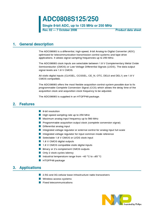
ADC0808S125/250
Single 8-bit ADC, up to 125 MHz or 250 MHz
Rev. 02 — 7 October 2008 Product data sheet
1. General description
The ADC0808S is a differential, high-speed, 8-bit Analog-to-Digital Converter (ADC) optimized for telecommunication transmission control systems and tape drive applications. It allows signal sampling frequencies up to 250 MHz. The ADC0808S clock inputs are selectable between 1.8 V Complementary Metal Oxide Semiconductor (CMOS) or Low-Voltage Differential Signals (LVDS). The data output signal levels are 1.8 V CMOS. All static digital inputs (CLKSEL, CCSSEL, CE_N, OTC, DEL0 and DEL1) are 1.8 V CMOS compatible. The ADC0808S offers the most flexible acquisition control system possible due to its programmable Complete Conversion Signal (CCS) which allows the delay time of the acquisition clock and acquisition clock frequency to be adjusted. The ADC0808S is supplied in an HTQFP48 package.
V8A02解决方案用户手册V2.1

V8A02解决方案用户手册V2.1目录1. 文档说明 (6)1.1版本说明 (6)1.2专有名词 (6)2. 方案简介 (8)2.1方案概述 (8)2.2 功能特点 (8)2.2.1 支持DVI数据源输入 (8)2.2.2 支持宽屏等多种DVI输入分辨率 (8)2.2.3 发送卡超大带载 (8)2.2.4 功能强大的配套软件 (8)2.2.5 智能在线检测 (8)2.2.6 高刷新频率 (8)2.2.7 高灰度等级 (9)2.2.8 支持各种像素类型 (9)2.2.9 灵活支持各种模组 (9)2.2.10 多样的端口设置功能 (9)2.2.11箱体色度调整 (9)2.2.12 逐点校正功能 (9)2.2.13 集成测试功能 (9)2.2.14 联机配置数据 (9)2.2.15 智能维修 (10)2.2.16 环路备份功能 (10)2.2.17 在线升级固件安全可靠 (10)2.2.18 支持低电压输入 (10)2.2.19 配备指示灯及控制面板接口 (10)2.2.20 支持远距离传输 (10)2.2.21 支持音频传输及电源控制 (10)2.2.22 提供完整的二次开发接口 (10)2.2.24 支持内建PWM恒流 (10)2.2.25 支持低亮度高保真 (10)2.3产品清单 (11)3. 应用概述 (12)3.1 典型应用 (12)3.2 环路备份 (13)3.3 多发送卡 (14)4. 功能详解 (15)4.1 模组支持能力 (15)4.1.1 模组行、列数1~128以内任意 (16)4.1.2 模组数据类型 (16)4.1.3 模组内每扫描串移长度 (17)4.1.4 虚拟模组LED灯点位置多种排列方式 (17)4.2 箱体连接设置 (17)4.2.1 箱体内模组级联方式 (17)4.2.2 端口扩展 (18)4.2.3 端口对开 (19)4.2.4 端口逆序 (20)4.2.5 端口偏移 (20)4.2.6 箱体带载高度、宽度 (20)4.2.7 箱体显示起始的行、列位置 (21)4.2.8 箱体无信号输入时显示内容设置 (21)4.2.9 箱体级联数量 (21)4.2.10 箱体色度调整 (21)4.2.11 箱体逐点色度校正 (22)4.2.12 箱体测试功能 (22)4.3 屏体参数调节 (23)4.3.1 多个LED屏设置 (23)4.3.3 虚拟LED屏的实效果 (24)4.3.4 LED屏亮度调节 (25)4.3.5 LED屏对比度调节 (26)4.3.6 LED屏色温调节 (26)4.3.7 关闭LED屏显示 (27)4.3.8 锁定LED屏内容 (27)4.3.9 LED屏环境监控 (27)4.4 显示性能参数说明 (30)4.4.1 灰度等级 (30)4.4.2 刷新频率 (31)4.4.3 亮度效率 (31)4.4.4 最小OE (31)4.5 发送卡带载 (31)4.6 在线检测 (34)4.7 系统升级 (34)4.8 智能维修 (36)4.8.1 接收卡更换 (36)4.8.2模组替换 (37)5. 使用说明 (39)5.1 连接硬件 (39)5.1.1 发送卡安装方法 (39)5.1.2 接收卡安装方法 (39)5.1.3 多功能卡安装方法 (39)5.2 安装软件 (40)5.2.1 配置要求 (40)5.2.2 安装步骤 (40)5.3 系统设置 (40)5.3.1 显卡设置 (40)5.3.2系统设置 (43)6. 附录 (55)6.1 设备推荐型号 (55)6.1.1 DVI复制器 (55)6.2 选用线缆清单 (55)6.2.1 HDMI转DVI线缆 (55)6.2.2 音频线 (56)6.2.3 双绞线 (56)6.2.4 光纤 (56)1. 文档说明1.1版本说明版本日期说明V2.0 2013-01-09 升级自1.71版本V2.1 2013-07-15 新增接收卡产品1.2专有名词以下是本文中使用的专用术语及解释,便于读者更好的理解文章内容。●软件一系列按照特定顺序组织的计算机数据和指令的集合,本文中特指在计算机上运行的应用软件。
PCL-812PG卡说明
PCL-812PG多功能数据采集卡使用说明书第一章概述这一章介绍PCL-812PG的背景信息包括关键特性、扩展性能、产品说明书1.1绪论PCL-812PG 是IBM PC/XT/AT及其兼容机的高性能、高速、多功能数据采集卡。
整卡的详尽说明书及齐全的第三方卖主的软件支持是PCL-812PG广泛的应用于工业及实验室环境下。
主要应用于数据采集、过程控制、自动检测、工厂自动控制。
1.2关键特性。
16位单端模拟输入通道。
一个工业标准的12位逐位逼近式A/D转换器(HADC574Z)用于转换模拟量输入。
在DMA模式下最大的A/D采样速率为30KHz。
软件可编程模拟输入序列。
双极性电压+/- 5V, +/- 2.5 V, +/- 1.25V +/- 0.625 V +/- 0.3125 V。
三种A/D触发模式。
软件触发器。
可编程步测触发器。
外部脉冲触发器。
程序控制A/D转换器的数据传输,中断处理器或DMA转换。
一个Intel 8253-5可编程定时器/计数器可提供以0.5 MHz-35minutes/pulse步测输出(触发脉冲),定时器的时间基准为2 MHz。
一个16位计数器保留给用户设置应用。
两个12位单集成多极性D/A输出通道。
一路输出可由板内-5V或-10V参考电压产生0-5V 或0-10V范围的输出。
这个参考电压精度来源于A/D转换器的参考电压精度。
外部直流或交流参考电压同样也可以用于产生其它D/A 输出。
16位TTL/DTL兼容数字输入、输出通道1.3 扩展性能为了增强PCL-812PG功能,可以通过以下可选子卡来扩展其功能。
PCLD-789放大器/乘法器卡这个功能强的前置模拟信号调理卡能在一个A/D输入通道中多路传输16路信号。
高级的仪表化的放大器提供开关选择增益,分别为0.5, 1, 2, 10, 50, 100, 200, 1000或任何用户自定义。
PCLD-787八通道同步采样保持前置卡该卡允许在小于30 ns通道间采样时间偏差下进行八通道模拟信号的同步采集。
SM8122A中文资料

SM8122AWhite LED Driver ICOVERVIEWThe SM8122A is a high efficiency step-up DC/DC converter. Due to high voltage CMOS process realizing 25V output supply as maximum value, 2 to 6 lights of white LED connected in series can be lighted. By con-necting in series, current variation among LED is eliminated. Current value sent to white LED can be set by external resistors. In addition, brightness can also be adjusted by control to FB pin or CE pin. Since the SM8122A has an over voltage protection circuit built-in, it dispenses with the existing external ZD (zener diode). Besides, the switching frequency of the SM8122A is higher (2.0MHz) than the existing product (SM8121A), so that it can respond to lower inductance value.FEATURESI Boost-up control using PWMI 2 to 6 lights of white L ED (connected in series) lightedI Output current value can be set by external resis-tors (51Ω: 9.8mA, 33Ω: 15.2mA, 24Ω: 20.8mA) I Brightness adjustable by control to FB pin or CE pinI Current variation among LED decreased by high precisionI High efficient drive by step-up modelI Over voltage protection circuit built-inI Supply voltage range: 2.3 to 5.5VI Maximum output voltage: 25VI Quiescent current: 820µA (typ)I Standby current: 1.0µA (max)I R ON (Switching MOS-Tr): 2Ω (typ)I Switching frequency: 2.0MHz (typ)I Output current detection accuracy: ± 2%I Package: SOT23-6W (SM8122AH)MSON-6 (SM8122AD) APPLICATIONSI Cellular phoneI PagerI Digital still cameraI Handy terminalI PDAsI Portable gamesI White LED driveI LCD bias supplyI Flash memory supplyORDERING INFORMATION PINOUT (Top view)I SOT23-6W I MSON-6Device Package SM8122AH SOT23-6W SM8122AD MSON-6SWVOUTFB123VDDCE64VSS56431CESWVDD2VOUT5VSSFB元器件交易网SM8122APACKAGE DIMENSIONS(Unit: mm)ISOT23-6WIMSON-6+ 0.1元器件交易网SM8122ABLOCK DIAGRAMPIN DESCRIPTIONNumberName I/O DescriptionSOT23-6WMSON-6 12SW O Coil switching 26VOUT I Output voltage detection34FB I Feed back (Output current detection)43CE Ip 11.Input with built-in pull-down resistorChip enable (High active)55VSS –GND 61VDD–Power supplyCEVDDFB元器件交易网SM8122ASPECIFICATIONSAbsolute Maximum RatingsElectrical CharacteristicsV DD = 3.6V , V SS = 0V , Ta = 25 ° C unless otherwise notedParameterSymbol Rating Unit Supply voltage range V DD − 0.3 to 6.5V Input voltage range V IN V SS – 0.3 to V DD + 0.3V SW output voltage range V SW –0.3 to 30V SW input current I SW 500mA Power dissipationP D 250 (Ta = 25 ° C)mW Operating temperature range T opr –40 to 85 ° C Storage temperature rangeT stg− 55 to 125° CParameterPin Symbol ConditionRatingUnit min typ max Supply voltage VDD V DD 2.3 3.6 5.5V Maximum output voltage SW V OUT ––25V Standby current VDD I STB V CE = 0V –– 1.0 µ A Quiescent current VDD I DD V FB = 1.0V –200400 µ A V FB = 0V–8201600 µ A SW-Tr ON resister SW R ON I SW = 100mA, V DD = 3.6V – 2.0 3.0 Ω SW-Tr leak current SW I LEAK V SW = V DD –– 1.0 µ A Switching frequency SW f OSC V FB = 0V 1.8 2.0 2.2MHz Maximum duty SW Duty V FB = 0V758590%Input voltageCE V IH 2.0––V V IL ––0.6V Input currentCEI CE V CE = 3.6V – 5.010 µ A FB I FB V FB = 0.5V –1.0– 1.0 µ A VOUTI VOUT V OUT = 25V 6082120 µ A Soft-start time SW T SS1 Switching stop time 102070 µ s T SS2 Maximum duty restriction time –500– µ s FB voltage FB V FB 0.490.500.51V Coil inductance SW L SW – 4.710 µ H Over voltage detection VOUTV OV 2530.536V Over voltage detection releaseV OVR2328.5–V元器件交易网SM8122AOPERATION OVERVIEWThe SM8122A basic structure is a step-up DC/DC converter. The booster control employs Pulse Width Modu-lation (PWM) which controls the pulse duty cycle (85% max.) at constant frequency (2.0MHz typ.). The LED current is set by a current-setting resistor R1 connected between pins FB (with stable voltage of 0.5V typ.) and VSS.When the switching transistor SW-Tr is ON, energy is stored in the inductor L. When SW-Tr is rapidly switched OFF, the energy stored in the inductor generates a voltage across the terminals of the inductor. The induced voltage, after being added to the input voltage, turns ON the Schottky barrier diode SBD and the stored energy is transferred to the output capacitor. This sequence of events continues repeatedly, boosting the output voltage.The SM8122A features a built-in soft-start function. The soft-start time is approximately 500 µs from after the chip enable input CE rising edge. During this interval, the maximum duty is restricted.L C V INOUT µF元器件交易网SM8122AOVP (Over Voltage Protection)SM8122A is always monitoring the VOUT terminal voltage in order to protect itself from the stress of V OUT over voltage. If SM8122A detects the V OUT over voltage, it immediately stop the switching of the inductor drive transistor. After the VOUT terminal voltage decreases below the release voltage, SM8122A restarts switching the inductor drive transistor. The over voltage is set as approximately 30.5V , the release voltage is approximately 28.5V .Selecting the Current-setting Resistor (R1)The SM8122A control stabilizes the voltage on pin FB (0.5V typ.). Hence, the current-setting resistor R1 con-nected between FB and VSS sets the LED current I LED , where the resistance R1 is given by the following equation.R1 = 0.5 / ILED30.5V28.5VV O U TLED =0.5/R1元器件交易网SM8122ASelecting the Inductor (L)The inductor DC resistance affects the power efficiency, therefore a low DC resistance inductor is recom-mended. Note also that the peak inductor current I peak should not exceed the inductor maximum current rating. In pulsed current mode control, the peak inductor current I peak is given by the following equation.I peak = (V IN× T ON) / LFor example, if the input voltage V IN is 3.6V, the inductance L is 4.7µH, and the SW-Tr ON time T ON is 2MHz × 85% = 0.425µs, then the peak inductor current I peak is (3.6 × 0.425 × 10-6) / (4.7 × 10⁻⁶) = 0.326A = 326mA. Selecting the Capacitors (C IN, C OUT)The recommended capacitances for use with the SM8122A are 4.7µF ceramic input capacitor C IN and 1.0µF ceramic output capacitor C OUT. The capacitor ESR ratings affect the ripple voltage, therefore capacitors with low ESR rating are recommended. The input capacitor should be mounted close to the SM8122A IC. Note that the capacitor voltage ratings should be selected to provide sufficient margin for the applied input and output voltages.For example, if a lithium-ion battery (2.5 to 4.5V) is connected to the input and 3 white LEDs connected in series at the output draw 20mA, then the maximum input voltage is 4.5V and the maximum output voltage is (4.0V × 3 LEDs) + 0.5V = 12.5V. Therefore, the input capacitor should have a voltage rating of 6V, and the output capacitor should have a voltage rating of 16V.Selecting the Rectifier Schottky Barrier Diode (SBD)The rectifier schottky barrier diode forward-direction voltage drop affects the power efficiency, therefore a Schottky barrier diode with low forward-direction voltage drop is recommended. Note that the diode should be selected to provide sufficient margin for the rated current and reverse-direction withstand voltage.Board Layout NotesThe following precautions should be followed for stable device operation.I The inductor L and Schottky barrier diode SBD should be connected close to the pin SW using thick, short circuit wiring.I The input capacitor C IN should be mounted close to the IC.I The IC supply voltage V DD wiring and inductor supply wiring should be isolated, reducing any common impedances.I The ground wiring should be connected at a single point, reducing any common impedances.V IN LED元器件交易网BRIGHTNESS ADJUSTMENT Brightness Adjustment using FB PinThe LED brightness can be adjusted using an input DC control voltage connected through resistor R3 to the FB pin. Alternatively, the brightness can be controlled by a PWM signal by adding a low-pass filter comprising resistor R4 and capacitor C1. The PWM signal frequency range is determined by the low-pass filter coeffi-cients. For example, the recommended values for resistor R4 (50k Ω) and capacitor C1 (0.1µF) provide a PWM signal frequency range of 1kHz to 1MHz.Brightness adjustment using FB pin (DC voltage input)When the brightness is controlled by DC voltage (V DC ) connected to resistor R3, the LED current (I LED ) is given by equation 1.If the values R1 = 30Ω, R2 = 20k Ω, R3 = 100k Ω, V FB = 0.5V , and V DC = 0V are inserted in equation 1, the LED current I LED = 20mA, as shown in equation 2.If the values R1 = 30Ω, R2 = 20k Ω, R3 = 100k Ω, V FB = 0.5V , and V DC = 3V are inserted in equation 1, the LED current I LED = 0mA, as shown in equation 3.Taking the above diagram as an example, inserting the values R1 = 30Ω, R2 = 20k Ω, R3 = 100k Ω, V FB = 0.5V ,and V DC = 0 to 3V into equation 1 gives the maximum LED current I LED of 20mA when V DC = 0V (equation 2) and the minimum LED current I LED of 0mA when V DC = 3V (equation 3).Brightness adjustment circuit using FB pin(DC voltage input)ΩV DC voltage vs. LED current051015200.00.51.01.52.02.53.0DC voltage [V]L E D c u r r e n t [m A ]R1R2 × (V DC − V FB )R3I LED =V FB − (1)20,000 × (0 − 0.5)100,0003030I LED===0.5 −0.620mA (2)20,000 × (3 − 0.5)100,0003030I LED===0.5 −0mA (3)Brightness adjustment using FB pin (PWM signal input)When the brightness is controlled by PWM signal (V PWM × Duty), the LED current (I LED ) is given by equa-tion 4.If the values R1 = 30Ω, R2 = 20k Ω, R3 = 50k Ω, R4 = 50k Ω, V FB = 0.5V , V PWM = 3V , and Duty = 0% are inserted in equation 4, the LED current I LED = 20mA, as shown in equation 5.If the values R1 = 30Ω, R2 = 20k Ω, R3 = 50k Ω, R4 = 50k Ω, V FB = 0.5V , V PWM = 3V , and Duty = 100% are inserted in equation 4, the LED current I LED = 0mA, as shown in equation 6.Taking the above diagram as an example, inserting the values R1 = 30Ω, R2 = 20k Ω, R3 = 50k Ω, R4 = 50k Ω,V FB = 0.5V , V PWM = 3V , and Duty = 0 to 100% into equation 4 gives the maximum LED current I LED of 20mA when Duty = 0% (equation 5) and the minimum LED current I LED of 0mA when Duty = 100% (equa-tion 6).Brightness adjustment circuit using FB pin(PWM signal input)ΩV PWM signal vs. LED current051015200.00.51.01.52.02.53.0V PWM × Duty [V]L E D c u r r e n t [m A ]R2 × (V PWM × Duty − V FB )R3 +R4R1I LED =V FB − (4)3030I LED ===20,000 × (3 × 0 − 0.5)50,000 + 50,0000.5 −0.620mA (5)3030I LED ===20,000 × (3 × 1 − 0.5)50,000 + 50,0000.5 −0mA (6)Brightness Adjustment using CE PinThe LED average current can be adjusted by controlling the duty of a PWM signal input on the CE pin. When CE goes from LOW to HIGH, the soft start function operates (with 500µs constant soft start time) and, there-fore, the LED average current ratio for a given PWM signal duty falls with increasing PWM signal frequency.Taking this into consideration, the recommended PWM control signal has a frequency range of 100 to 400Hz with duty cycle range of 10 to 90%.When adjusting the brightness using the CE pin, a ripple voltage synchronized to the PWM signal is generated across the output capacitor C OUT . The amplitude of the ripple voltage is determined by the number of LEDs and their forward-bias voltage drop characteristics. If a ceramic capacitor is used for the output capacitor C OUT , an audible noise may be generated due to the ceramic capacitor ’s piezoelectric effect. The audible noise level depends on the ceramic capacitor (capacitance, bias dependency, withstand voltage etc.), LEDs (number,forward-bias voltage drop etc.), and mounting board (thickness, mounting conditions etc.), and thus should be veri fied under actual conditions.Brightness adjustment circuit using CE pinΩVPWM signal duty vs. LED average current10200.05.010.015.020.0030405060708090100PWM signal duty [%]A v e r a g e L E D c u r r e n t [mA ]Alternatively, a tantalum capacitor or film capacitor with low piezoelectric effect can be used as the output capacitor C OUT to minimize the noise level, or the brightness can be adjusted using the FB pin as described earlier. The audible noise generated when using the CE pin is not an inherent phenomena of the SM8122A device, but of the brightness adjustment method employed.Output voltage with LEDs ONOutput voltage with LEDsOFFCE input signal and output ripple voltageCurrent Switching using External TransistorsIf only a few brightness steps are required, the LED current can be adjusted by switching the LED current set-ting resistance using external transistors (Tr).ΩV Select signal 2Select signal 1I LEDLow Low 2mALow High 2 + 5 = 7mA HighLow 2 + 12.5 = 14.5mA HighHigh2 + 5 + 12.5 = 19.5mARECOMMEND PATTERN SOT23-6WMSON-6Footprint pattern1.Footprint patternçMetalmask patternNC0323AE2005.05。
AD2S80A中文手册
最小值
典型值
150
最大值
30
单位
ns
BUSY3 检测 宽度 负载 DIRECTION3 检测 最大负载 RIPPLE CLOCK3 检测 宽度 复位 负载 数字输入 高电压VIH 低电压VIL 数字输入 高电流IIH 低电流IIL
200
600
ns
LSTTL
3
LSTTL
300 3 2.0 0.8 V V LSTTL
ADI中文版数据手册是英文版数据手册的译文,敬请谅解翻译中可能存在的语言组织或翻译错误,ADI不对翻译中存在的差异或由此产生的错误负责。如需确认任何词语的准确性,请参考ADI提供 的最新英文版数据手册。
BYTE SELECT 5V DIG GND BUSY DIR INHIBIT
SC1 SC2
ENABLE
AD2S80A
SEGMENT SWITCHING R-2R DAC
SIN I/P SIG GND COS I/P ANALOG GND RIPPLE CLK DATA LOAD +12V –12V
A1
A3 PHASE SENSITIVE DETECTOR VCO DATA TRANSFER LOGIC
100 100
µA
µA
数字输入 低电压VIL 低电流IIL 数字输出 高电压VOH
1.0 –400
V µA
2.4 0.4
V V
低电压VOL
三态泄漏 电流IL
±100 ±100
µA µA
注释 1 指小信号带宽。 2 输出失调取决于R6的值。 3 参考时序图。 规格如有变更恕不另行通知。 所有最小值和最大值规格均保证实现。以粗体显示的规格是最终电气测试时,在所有成品上测得的。
许继操作箱ZFZ-812A

0XJ 463 284第 2 页共 33 页旧底图总号底图总号签字日期1概述1.1装置用途装置作为分相断路器操作的辅助控制回路,适用于220kV及以上具有双跳闸线圈的一台断路器控制操作之用。
1.2 装置综述装置共一层箱,包括十六个插件,均采用插件形式,保证了配置的灵活方便,有电压切换插件及ZJ备用继电器回路插件,TXJ信号回路插件,HHJ、ZHJ、SHJ合闸继电器回路插件,TBJ防跳继电器回路插件,两个三跳继电器回路插件,两个HWJ合位继电器回路插件,TWJ跳位继电器回路插件, YJJ压力监视回路插件。
装置除能正确反映跳、合情况还设有防止跳跃的防跳闭锁继电器TBJ,利用其本身特点和触点不同的回路连接,能防止断路器多次“跳—合”现象。
同时,可实现电压的自动切换,保证双母线(带旁路)接线系统上所连接的电气元件在运行时,其一次系统和二次系统相对应,以免保护及自动装置发生误动或拒动。
为了防止在运行中由于控制跳闸的气(液)压触点接触不良造成气(液)压闭锁环节失灵,压力监视继电器1YJJ、2YJJ 、3YJJ、4YJJ还设有预告信号。
2 技术参数2.1 基本数据2.1.1 额定数据a.直流电压:220V或110V;b.跳闸保持电流:0.25A、0.5A、1A;c.合闸保持电流:0.25A、0.5A、1A。
注:1A及1A以上选用1A规格2.1.2 装置功率消耗在额定直流电压下,直流电压回路功率消耗正常情况下不大于60W。
2.1.3触点性能装置的出口触点,在电压不大于250V,电流不大于0.5A,时间常数为5ms±0.75ms的直流有感负荷电路中,断开容量为50W,长期允许通过电流为5A。
装置的信号触点,在电压不大于250V,电流不大于0.5A,时间常数为5ms±0.75ms的直流有感负荷电路中,断开容量为30W,长期允许通过电流为3A。
2.1.4装置约重20kg。
2.2 绝缘性能2.2.1 绝缘电阻0XJ 463 284第 3 页共 33 页旧底图总号底图总号签字日期 装置所有电路对外壳及电气上无联系的各电路之间的绝缘电阻在正常校验的标准大气条件下,不小于100MΩ。
AD812中文资料
元器件交易网
AD812–SPECIFICATIONS
Dual Supply (@ T = +25؇C, R = 150 ⍀, unless otherwise noted)
A L
Model Conditions DYNAMIC PERFORMANCE –3 dB Bandwidth G = +2, No Peaking Gain = +1 G = +2 G = +2, RL = 1 kΩ 20 V Step G = –1, RL = 1 kΩ G = –1, RL = 1 kΩ VO = 3 V Step VO = 10 V Step fC = 1 MHz, RL = 1 kΩ f = 10 kHz f = 10 kHz, +In f = 10 kHz, –In NTSC, G = +2, RL = 150 Ω VS ±5 V ± 15 V ± 15 V ±5 V ± 15 V ±5 V ± 15 V ±5 V ± 15 V ±5 V ± 15 V ± 15 V ± 5 V, ± 15 V ± 5 V, ± 15 V ± 5 V, ± 15 V ±5 V ± 15 V ±5 V ± 15 V ± 5 V, ± 15 V TMIN –TMAX Offset Drift –Input Bias Current TMIN –T MAX +Input Bias Current Open-Loop Voltage Gain TMIN –T MAX VO = ± 2.5 V, RL = 150 Ω TMIN –T MAX VO = ± 10 V, RL = 1 kΩ TMIN –T MAX VO = ± 2.5 V, RL = 150 Ω TMIN –T MAX VO = ± 10 V, RL = 1 kΩ TMIN –T MAX +Input –Input +Input ± 5 V, ± 15 V ± 5 V, ± 15 V ± 5 V, ± 15 V ±5 V ± 15 V ±5 V ± 15 V 68 69 76 75 350 270 450 370 Min 50 75 100 20 25 275 1400
AD8253ARMZ-R7,AD8253ARMZ-R7,AD8253ARMZ-R7,AD8253ARMZ-RL,AD8253ARMZ, 规格书,Datasheet 资料
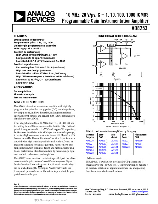
10 MHz, 20 V/μs, G = 1, 10, 100, 1000 i CMOSProgrammable Gain Instrumentation AmplifierAD8253 Rev. AInformation furnished by Analog Devices is believed to be accurate and reliable. However, noresponsibility is assumed by Analog Devices for its use, nor for any infringements of patents or other rights of third parties that may result from its use. Specifications subject to change without notice. No license is granted by implication or otherwise under any patent or patent rights of Analog Devices. T rademarks and registered trademarks are the property of their respective owners. One Technology Way, P.O. Box 9106, Norwood, M A 02062-9106, U.S.A. Tel: 781.329.4700 Fax: 781.461.3113 ©2008 Analog Devices, Inc. All rights reserved.FEATURESSmall package: 10-lead MSOPProgrammable gains: 1, 10, 100, 1000Digital or pin-programmable gain settingWide supply: ±5 V to ±15 VExcellent dc performanceHigh CMRR: 100 dB (minimum), G = 100Low gain drift: 10 ppm/°C (maximum)Low offset drift: 1.2 μV/°C (maximum), G = 1000 Excellent ac performanceFast settling time: 780 ns to 0.001% (maximum)High slew rate: 20 V/μs (minimum)Low distortion: −110 dB THD at 1 kHz,10 V swingHigh CMRR over frequency: 100 dB to 20 kHz (minimum) Low noise: 10 nV/√Hz, G = 1000 (maximum)Low power: 4 mAAPPLICATIONSData acquisitionBiomedical analysisTest and measurementGENERAL DESCRIPTIONThe AD8253 is an instrumentation amplifier with digitally programmable gains that has gigaohm (GΩ) input impedance, low output noise, and low distortion, making it suitable for interfacing with sensors and driving high sample rate analog-to-digital converters (ADCs).It has a high bandwidth of 10 MHz, low THD of −110 dB, and fast settling time of 780 ns (maximum) to 0.001%. Offset drift and gain drift are guaranteed to 1.2 μV/°C and 10 ppm/°C, respectively, for G = 1000. In addition to its wide input common voltage range, it boasts a high common-mode rejection of 100 dB at G = 1000 from dc to 20 kHz. The combination of precision dc performance coupled with high speed capabilities makes the AD8253 an excellent candidate for data acquisition. Furthermore, this monolithic solution simplifies design and manufacturing and boosts performance of instrumentation by maintaining a tight match of internal resistors and amplifiers.The AD8253 user interface consists of a parallel port that allows users to set the gain in one of two different ways (see Figure 1 for the functional block diagram). A 2-bit word sent via a bus can be latched using the WR input. An alternative is to use transparent gain mode, where the state of logic levels at the gain port determines the gain.FUNCTIONAL BLOCK DIAGRAMS S+IN6983-1Figure 1.8070605040302010–10–201k10k100k1M10M100MFREQUENCY (Hz)GAIN(dB)6983-23Figure 2. Gain vs. FrequencyTable 1. Instrumentation Amplifiers by CategoryGeneralPurposeZeroDriftMilGradeLowPowerHigh SpeedPGAAD82201AD82311AD620AD6271AD8250AD8221AD85531AD621AD6231AD8251AD8222AD85551AD524AD82231AD8253AD82241AD85561AD526AD8228AD85571AD6241 Rail-to-rail output.The AD8253 is available in a 10-lead MSOP package and is specified over the −40°C to +85°C temperature range, making it an excellent solution for applications where size and packing density are important considerations.AD8253Rev. A | Page 2 of 24TABLE OF CONTENTSFeatures .............................................................................................. 1 Applications ....................................................................................... 1 General Description ......................................................................... 1 Functional Block Diagram .............................................................. 1 Revision History ............................................................................... 2 Specifications ..................................................................................... 3 Timing Diagram ........................................................................... 5 Absolute Maximum Ratings ............................................................ 6 Maximum Power Dissipation ..................................................... 6 ESD Caution .................................................................................. 6 Pin Configuration and Function Descriptions ............................. 7 Typical Performance Characteristics ............................................. 8 Theory of Operation ...................................................................... 16 Gain Selection ............................................................................. 16 Power Supply Regulation and Bypassing ................................ 18 Input Bias Current Return Path ............................................... 18 Input Protection ......................................................................... 18 Reference Terminal .................................................................... 19 Common-Mode Input Voltage Range ..................................... 19 Layout .......................................................................................... 19 RF Interference ........................................................................... 19 Driving an Analog-to-Digital Converter ................................ 20 Applications Information .............................................................. 21 Differential Output .................................................................... 21 Setting Gains with a Microcontroller ...................................... 21 Data Acquisition ......................................................................... 22 Outline Dimensions ....................................................................... 23 Ordering Guide .. (23)REVISION HISTORY8/08—Rev. 0 to Rev. AChanges to Ordering Guide (23)7/08—Revision 0: Initial VersionAD8253SPECIFICATIONS+V S = +15 V, −V S = −15 V, V REF = 0 V @ T A = 25°C, G = 1, R L = 2 kΩ, unless otherwise noted.Table 2.Parameter Conditions Min Typ Max Unit COMMON-MODE REJECTION RATIO (CMRR)CMRR to 60 Hz with 1 kΩ Source Imbalance +IN = −IN = −10 V to +10 VG = 1 80 100 dBG = 10 96 120 dBG = 100 100 120 dBG = 1000 100 120 dB CMRR to 20 kHz1+IN = −IN = −10 V to +10 VG = 1 80 dBG = 10 96 dBG = 100 100 dBG = 1000 100 dB NOISEVoltage Noise, 1 kHz, RTIG = 1 45 nV/√HzG = 10 12 nV/√HzG = 100 11 nV/√HzG = 1000 10 nV/√Hz0.1 Hz to 10 Hz, RTIG = 1 2.5 μV p-pG = 10 1 μV p-pG = 100 0.5 μV p-pG = 1000 0.5 μV p-p Current Noise, 1 kHz 5 pA/√Hz Current Noise, 0.1 Hz to 10 Hz 60 pA p-p VOLTAGE OFFSETOffset RTI V OS G = 1, 10, 100, 1000 ±150 + 900/G μV Over Temperature T = −40°C to +85°C ±210 + 900/G μV Average TC T = −40°C to +85°C ±1.2 + 5/G μV/°C Offset Referred to the Input vs. Supply (PSR) V S = ±5 V to ±15 V ±5 + 25/G μV/V INPUT CURRENTInput Bias Current 5 50 nA Over Temperature2T = −40°C to +85°C 40 60 nA Average TC T = −40°C to +85°C 400 pA/°C Input Offset Current 5 40 nA Over Temperature T = −40°C to +85°C 40 nA Average TC T = −40°C to +85°C 160 pA/°C DYNAMIC RESPONSESmall-Signal −3 dB BandwidthG = 1 10 MHzG = 10 4 MHzG = 100 550 kHzG = 1000 60 kHz Settling Time 0.01% ΔOUT = 10 V stepG = 1 700 nsG = 10 680 nsG = 100 1.5 μsG = 1000 14 μsRev. A | Page 3 of 24AD8253Rev. A | Page 4 of 24AD8253Rev. A | Page 5 of 24Parameter Conditions Min Typ Max UnitPOWER SUPPLY Operating Range±5 ±15 V Quiescent Current, +I S 4.6 5.3 mA Quiescent Current, −I S 4.5 5.3mA Over Temperature T = −40°C to +85°C 6 mA TEMPERATURE RANGE Specified Performance−40 +85 °C1 See Figure 20 for CMRR vs. frequency for more information on typical performance over frequency.2Input bias current over temperature: minimum at hot and maximum at cold. 3See Figure 30 for input voltage limit vs. supply voltage and temperature. 4See Figure 32, Figure 33, and Figure 34 for output voltage swing vs. supply voltage and temperature for various loads. 5Add time for the output to slew and settle to calculate the total time for a gain change.TIMING DIAGRAMA0, A1WR06983-003Figure 3. Timing Diagram for Latched Gain Mode (See the Timing for Latched Gain Mode Section)AD8253Rev. A | Page 6 of 24ABSOLUTE MAXIMUM RATINGSTable 3.Parameter RatingSupply Voltage ±17 VPower Dissipation See Figure 4Output Short-Circuit CurrentIndefinite 1 Common-Mode Input Voltage ±V S Differential Input Voltage ±V S Digital Logic Inputs±V SStorage Temperature Range –65°C to +125°C Operating Temperature Range 2–40°C to +85°C Lead Temperature (Soldering 10 sec) 300°C Junction Temperature140°C θJA (4-Layer JEDEC Standard Board) 112°C/W Package Glass Transition Temperature140°C1 Assumes the load is referenced to midsupply.2Temperature for specified performance is −40°C to +85°C. For performance to +125°C, see the Typical Performance Characteristics section.Stresses above those listed under Absolute Maximum Ratings may cause permanent damage to the device. This is a stress rating only; functional operation of the device at these or any other conditions above those indicated in the operationalsection of this specification is not implied. Exposure to absolute maximum rating conditions for extended periods may affect device reliability.MAXIMUM POWER DISSIPATIONThe maximum safe power dissipation in the AD8253 package is limited by the associated rise in junction temperature (T J ) on the die. The plastic encapsulating the die locally reaches the junction temperature. At approximately 140°C, which is the glass transition temperature, the plastic changes its properties. Even temporarily exceeding this temperature limit can change the stresses that the package exerts on the die, permanently shifting the parametric performance of the AD8253. Exceeding a junction temperature of 140°C for an extended period can result in changes in silicon devices, potentially causing failure. The still-air thermal properties of the package and PCB (θJA ), the ambient temperature (T A ), and the total power dissipated in the package (P D ) determine the junction temperature of the die. The junction temperature is calculated as()JA D A J θP T T ×+=The power dissipated in the package (P D ) is the sum of the quiescent power dissipation and the power dissipated in the package due to the load drive for all outputs. The quiescent power is the voltage between the supply pins (V S ) times the quiescent current (I S ). Assuming the load (R L ) is referenced tomidsupply, the total drive power is V S /2 × I OUT , some of which isdissipated in the package and some of which is dissipated in theload (V OUT × I OUT ). The difference between the total drive power and the load power is the drive power dissipated in the package.P D = Quiescent Power + (Total Drive Power − Load Power )()L 2OUT L OUTS S S D R V –R V2V I V P ⎟⎟⎠⎞⎜⎜⎝⎛×+×= In single-supply operation with R L referenced to −V S , the worstcase is V OUT = V S /2.Airflow increases heat dissipation, effectively reducing θJA . In addition, more metal directly in contact with the package leads from metal traces through holes, ground, and power planes reduces the θJA .Figure 4 shows the maximum safe power dissipation in the package vs. the ambient temperature on a 4-layer JEDEC standard board.2.001.751.501.251.000.750.500.250–40–20120100806040200M A X I M U M P O W E R D I S S I P A T I O N (W )AMBIENT TEMPERATURE (°C)06983-004Figure 4. Maximum Power Dissipation vs. Ambient TemperatureESD CAUTIONAD8253Rev. A | Page 7 of 24PIN CONFIGURATION AND FUNCTION DESCRIPTIONS–IN DGND –V S A0A1+INREF+V S OUT WRAD8253TOP VIEW(Not to Scale)1234510987606983-005Figure 5. 10-Lead MSOP (RM-10) Pin ConfigurationAD8253Rev. A | Page 8 of 24TYPICAL PERFORMANCE CHARACTERISTICST A @ 25°C, +V S = +15 V , −V S = −15 V , R L = 10 kΩ, unless otherwise noted.CMRR (µV/V)21006983-006N U M B E R O F U N I T S180150120906030–60–40–20020INPUT OFFSET CURRENT (nA)240120180601502109030604020006983-009N U M B E R O F U N I T S–60–20–40Figure 6. Typical Distribution of CMRR, G = 1 Figure 9. Typical Distribution of Input Offset CurrentINPUT OFFSET VOLTAGE, V OSI , RTI (µV)180120150200100006983-007N U M B E R O F U N I T S–200–10006983-0101100kFREQUENCY (Hz)N O I S E (n V /√H z )101001k10k8070605040302010Figure 10. Voltage Spectral Density Noise vs. FrequencyFigure 7. Typical Distribution of Offset Voltage, V OSI 06983-011INPUT BIAS CURRENT (nA)30020025015010050906030006983-008N U M B E R O F U N I T S–90–30–60Figure 11. 0.1 Hz to 10 Hz RTI Voltage Noise, G = 1Figure 8. Typical Distribution of Input Bias CurrentAD8253Rev. A | Page 9 of 2406983-012Figure 12. 0.1 Hz to 10 Hz RTI Voltage Noise, G = 1000 06983-01318011FREQUENCY (Hz)N O I S E (p A /√H z )00k 101001k 10k 161412108642Figure 13. Current Noise Spectral Density vs. Frequency 06983-014Figure 14. 0.1 Hz to 10 Hz Current Noise 201816141210864200.010.1110WARM-UP TIME (Minutes)C H A N G E I N I N P U T O F F S E T V O L T A G E (µV )06983-015Figure 15. Change in Input Offset Voltage vs. Warm-Up Time, G = 10001401201008040600101M06983-016FREQUENCY (Hz)P S R R (d B )1001k 10k 100k 20Figure 16. Positive PSRR vs. Frequency, RTI1401201008040600101M06983-017FREQUENCY (Hz)P S R R (d B )1001k 10k 100k 20Figure 17. Negative PSRR vs. Frequency, RTIAD8253Rev. A | Page 10 of 2420100–10–20–30–40–50–6012.0I B +10.59.07.56.04.53.01.50–15–10–5051015COMMON-MODE VOLTAGE (V)I N P U T B I A S C U R R E N T (n A )I N P U T O F F S E T C U R R E N T (n A )06983-018I B –I OSFigure 18. Input Bias Current and Offset Current vs. Common-Mode Voltage 302520151050–10–5–60–40–20020406080100120140TEMPERATURE (°C)I N P U T B I A S C U R R E N T A N D O F F S E T C U R R E N T (n A )06983-019I B +I B –I OS Figure 19. Input Bias Current and Offset Current vs. Temperature 012010080604020106983-020FREQUENCY (Hz)C M R R (d B )1001k 10k 100k 1MFigure 20. CMRR vs. Frequency120100806040201006983-021FREQUENCY (Hz)C M R R (d B)1001k 10k 100k 1MFigure 21. CMRR vs. Frequency, 1 kΩ Source Imbalance–15–5013006983-022TEMPERATURE (°C)C M R R (µV /V )10155–5–10–30–101030507090110Figure 22. CMRR vs. Temperature, G = 180706050403020100–10–201k10k100k 1M 10M 100MFREQUENCY (Hz)G A I N (d B )006983-023Figure 23. Gain vs. Frequency40302010–10–300–20–40–10–8–6–4–2024681006983-024N O N L I N E A R I T Y (10p p m /D I V )OUTPUT VOLTAGE (V)Figure 24. Gain Nonlinearity, G = 1, R L = 10 kΩ, 2 kΩ, 600 Ω 40302010–10–300–20–40–10–8–6–4–2024681006983-025N O N L I N E A R I T Y (10p p m /D I V )OUTPUT VOLTAGE (V)Figure 25. Gain Nonlinearity, G = 10, R L = 10 kΩ, 2 kΩ, 600 Ω 80604020–20–600–40–80–10–8–6–4–2024681006983-026N O N L I N E A R I T Y (10p p m /D I V )OUTPUT VOLTAGE (V)Figure 26. Gain Nonlinearity, G = 100, R L = 10 kΩ, 2 kΩ, 600 Ω400300200100–100–3000–200–400–10–8–6–4–2024681006983-027N O N L I N E A R I T Y (10 p p m /D I V )OUTPUT VOLTAGE (V)Figure 27. Gain Nonlinearity, G = 1000, R L = 10 kΩ, 2 kΩ, 600 Ω16–1606983-028OUTPUT VOLTAGE (V)I N P U T C O M M O N -M O D E V O L T A G E (V )1284–4–8–12–12–8–44812Figure 28. Input Common-Mode Voltage Range vs. Output Voltage, G = 116–16–161606983-029OUTPUT VOLTAGE (V)I N P U T C O M M O N -M O D E V O L T A G E (V )1284–4–8–12–12–8–44812Figure 29. Input Common-Mode Voltage Range vs. Output Voltage, G = 1000+V S –V S4106983-030SUPPLY VOLTAGE (±V S )I N P U T V O L T A G E (V )R E F E R R E D T O S U P P L Y V O L T A G E S6–1–2+2+168101214Figure 30. Input Voltage Limit vs. Supply Voltage, G = 1, V REF = 0 V, R L = 10 kΩ–1––100m–10–1–100µ–10µ10DIFFERENTIAL INPUT VOLTAGE (V)C U R R E N T (m A )06983-0311001101001Figure 31. Fault Current Draw vs. Input Voltage, G = 1000, R L = 10 kΩ +V S –V S4106983-032SUPPLY VOLTAGE (±V S )OU T P U T V O L T A G E S W I N G (V )R E F E R R E D T O S U P P L Y V O L T A G E S668101214–0.2–0.4–0.6–0.8–1.0–1.2+1.0+1.2+0.8+0.6+0.4+0.2Figure 32. Output Voltage Swing vs. Supply Voltage, G = 1000, R L = 2 kΩ +V S –V S4106983-033SUPPLY VOLTAGE (±V S )O U T P U T V O L T A G E S W I N G (V )R E F E R R E D T O S U P P L Y V O L T A G E S668101214–0.2–0.4–0.6–0.8–1.0+1.0+0.8+0.6+0.4+0.2Figure 33. Output Voltage Swing vs. Supply Voltage, G =1000, R L = 10 kΩ15–1510010k06983-034LOAD RESISTANCE (Ω)1k105–5–10O U T P U T V O L T A G E S W I N G (V )Figure 34. Output Voltage Swing vs. Load Resistance+V S –V S4106983-035OUTPUT CURRENT (mA)668101214–0.4–0.8–1.2–1.6–2.0+2.0+1.6+1.2+0.8+0.4O U T P U T V O L T A G E S W I N G (V )R E F E R R E D T O S U P P L Y V O L T A G E SFigure 35. Output Voltage Swing vs. Output Current06983-036Figure 36. Small-Signal Pulse Response for Various Capacitive Loads, G = 1069TIME (µs)Figure 37. Large-Signal Pulse Response and Settling Time, G = 1, R L= 10 kΩ06983-038TIME (µs)Figure 38. Large-Signal Pulse Response and Settling Time,G = 10, R L= 10 kΩ06983-039TIME (µs)Figure 39. Large-Signal Pulse Response and Settling Time,G = 100, R L= 10 kΩ06983-040TIME (µs)Figure 40. Large-Signal Pulse Response and Settling Time,G = 1000, R L= 10 kΩ06983-041Figure 41. Small-Signal Response,G = 1, R L = 2 kΩ, C L = 10006983-042Figure 42. Small-Signal Response, G = 10, R L = 2 kΩ, C L = 100 pF06983-043Figure 43. Small-Signal Response, G = 100, R L = 2 kΩ, C L = 100 pF06983-044Figure 44. Small-Signal Response, G = 1000, R L = 2 kΩ, C L = 100 pF 06983-045120014000STEP SIZE (V)T I M E (n s )10008006004002004681012141618Figure 45. Settling Time vs. Step Size, G = 1, R L = 10 kΩ06983-04612001400STEP SIZE (V)T I M E (n s )10008006004002004681012141618Figure 46. Settling Time vs. Step Size, G = 10, R L = 10 kΩ06983-04722STEP SIZE (V)T I M E (n s )10008006001800160014004002004681012141618Figure 47. Settling Time vs. Step Size, G = 100, R L = 10 kΩ06983-048STEP SIZE (V)T I M E (µs )1086181614424681012141618Figure 48. Settling Time vs. Step Size, G = 1000, R L = 10 kΩ0–10–20–30–40–50–60–70–80–90–120–110–100101M06983-049FREQUENCY (Hz)T H D + N (d B )1001k 10k 100k Figure 49. Total Harmonic Distortion vs. Frequency,10 Hz to 22 kHz Band-Pass Filter, 2 kΩ Load0–10–20–30–40–50–60–70–80–90–120–110–100101M06983-050FREQUENCY (Hz)T H D + N (d B )1001k 10k 100k Figure 50. Total Harmonic Distortion vs. Frequency, 10 Hz to 500 kHz Band-Pass Filter, 2 kΩ LoadTHEORY OF OPERATIONREFOUTSS 06983-061Figure 51. Simplified SchematicTransparent Gain ModeThe AD8253 is a monolithic instrumentation amplifier based on the classic 3-op-amp topology, as shown in Figure 51. It is fabricated on the Analog Devices, Inc., proprietary i CMOS® process that provides precision linear performance and a robust digital interface. A parallel interface allows users to digitally program gains of 1, 10, 100, and 1000. Gain control is achieved by switching resistors in an internal precision resistor array (as shown in Figure 51).The easiest way to set the gain is to program it directly via a logic high or logic low voltage applied to A0 and A1. Figure 52 shows an example of this gain setting method, referred to through-out the data sheet as transparent gain mode. Tie WR to the negative supply to engage transparent gain mode. In this mode, any change in voltage applied to A0 and A1 from logic low to logic high, or vice versa, immediately results in a gain change. is the truth table for transparent gain mode, and shows the AD8253 configured in transparent gain mode.Table 5Figure 52All internal amplifiers employ distortion cancellation circuitry and achieve high linearity and ultralow THD. Laser-trimmed resistors allow for a maximum gain error of less than 0.03% for G = 1 and a minimum CMRR of 100 dB for G = 1000. A pinout optimized for high CMRR over frequency enables the AD8253 to offer a guaranteed minimum CMRR over frequency of 80 dB at 20 kHz (G = 1). The balanced input reduces the parasitics that in the past had adversely affected CMRR performance.NOTE:1. IN TRANSPARENT GAIN MODE, WR IS TIED TO −V S .THE VOLTAGE LEVELS ON A0 AND A1 DETERMINE THE GAIN. IN THIS EXAMPLE, BOTH A0 AND A1 ARE SET TO LOGIC HIGH, RESULTING IN A GAIN OF 1000.06983-051GAIN SELECTIONThis section describes how to configure the AD8253 for basic operation. Logic low and logic high voltage limits are listed in the Specifications section. Typically, logic low is 0 V and logic high is 5 V; both voltages are measured with respect to DGND. Refer to the specifications table (Table 2) for the permissible voltage range of DGND. The gain of the AD8253 can be set using two methods: transparent gain mode and latched gain mode. Regardless of the mode, pull-up or pull-down resistors should be used to provide a well-defined voltage at the A0 and A1 pins.Figure 52. Transparent Gain Mode, A0 and A1 = High, G = 1000Latched Gain ModeSome applications have multiple programmable devices such as multiplexers or other programmable gain instrumentation amplifiers on the same PCB. In such cases, devices can share a data bus. The gain of the AD8253 can be set using WR as a latch, allowing other devices to share A0 and A1. shows a schematic using this method, known as latched gain mode. The AD8253 is in this mode when Figure 53WR is held at logic high or logic low, typically 5 V and 0 V , respectively. The voltages on A0 and A1 are read on the downward edge of the WR signal as it transitions from logic high to logic low. This latches in the logic levels on A0 and A1, resulting in a gain change. See the truth table listing in for more on these gain changes.Table 6NOTE:FROM LOGIC HIGH TO LOGIC LOW, THE VOLTAGES ON A0AND A1 ARE READ AND LATCHED IN, RESULTING IN AGAIN CHANGE. IN THIS EXAMPLE, THE GAIN SWITCHES TO G = 1000.06983-052Figure 53. Latched Gain Mode, G = 10001X = don’t care.On power-up, the AD8253 defaults to a gain of 1 when inlatched gain mode. In contrast, if the AD8253 is configured in transparent gain mode, it starts at the gain indicated by the voltage levels on A0 and A1 on power-up.Timing for Latched Gain ModeIn latched gain mode, logic levels at A0 and A1 must be held for a minimum setup time, t SU , before the downward edge of WR latches in the gain. Similarly, they must be held for a minimum hold time, t HD , after the downward edge of WR to ensure that the gain is latched in correctly. After t HD , A0 and A1 may change logic levels, but the gain does not change until the next downward edge of WR . The minimum duration that WR can be held high is t -HIGH , and t -LOW is the minimum duration that WR can be held low. Digital timing specifications are listed in The time required for a gain change is dominated by the settling time of the amplifier. A timing diagram is shown in . Table 2.Figure 54When sharing a data bus with other devices, logic levels applied to those devices can potentially feed through to the output of the AD8253. Feedthrough can be minimized by decreasing the edge rate of the logic signals. Furthermore, careful layout of the PCB also reduces coupling between the digital and analog portions of the board.A0, A106983-053Figure 54. Timing Diagram for Latched Gain ModePOWER SUPPLY REGULATION AND BYPASSINGThe AD8253 has high PSRR. However, for optimal performance, a stable dc voltage should be used to power the instrumentation amplifier. Noise on the supply pins can adversely affect per-formance. As in all linear circuits, bypass capacitors must be used to decouple the amplifier.Place a 0.1 μF capacitor close to each supply pin. A 10 μF tantalum capacitor can be used farther away from the part (see Figure 55) and, in most cases, it can be shared by other precision integrated circuits.06983-054Figure 55. Supply Decoupling, REF, and Output Referred to GroundINPUT BIAS CURRENT RETURN PATHThe AD8253 input bias current must have a return path to its local analog ground. When the source, such as a thermocouple, cannot provide a return current path, one should be created (see Figure 56).THERMOCOUPLE+V –V SCAPACITIVELY COUPLED +V SREFCC–V SAD8253TRANSFORMER+V SREF–V SAD8253INCORRECTCAPACITIVELY COUPLEDf HIGH-PASS THERMOCOUPLE+V TRANSFORMER–V SCORRECT06983-055Figure 56. Creating an I BIAS PathINPUT PROTECTIONAll terminals of the AD8253 are protected against ESD. An external resistor should be used in series with each of the inputs to limit current for voltages greater than 0.5 V beyond either supply rail. In such a case, the AD8253 safely handles a continuous 6 mA current at room temperature. For applications where the AD8253 encounters extreme overload voltages, external series resistors and low leakage diode clamps such as BAV199Ls, FJH1100s, or SP720s should be used.REFERENCE TERMINALThe reference terminal, REF, is at one end of a 10 kΩ resistor (see Figure 51). The instrumentation amplifier output is referenced to the voltage on the REF terminal; this is useful when the output signal needs to be offset to voltages other than its local analog ground. For example, a voltage source can be tied to the REF pin to level shift the output so that the AD8253 can interface with a single-supply ADC. The allowable reference voltage range is a function of the gain, common-mode input, and supply voltages. The REF pin should not exceed either +V S or −V S by more than 0.5 V .For best performance, especially in cases where the output is not measured with respect to the REF terminal, source imped-ance to the REF terminal should be kept low because parasiticresistance can adversely affect CMRR and gain accuracy.INCORRECTCORRECT06983-056Figure 57. Driving the Reference PinCOMMON-MODE INPUT VOLTAGE RANGEThe 3-op-amp architecture of the AD8253 applies gain and then removes the common-mode voltage. Therefore, internal nodes in the AD8253 experience a combination of both the gained signal and the common-mode signal. This combined signal can be limited by the voltage supplies even when the individual input and output signals are not. Figure 28 and Figure 29 show the allowable common-mode input voltage ranges for various output voltages, supply voltages, and gains.LAYOUTGroundingIn mixed-signal circuits, low level analog signals need to be isolated from the noisy digital environment. Designing with the AD8253 is no exception. Its supply voltages are referenced to an analog ground. Its digital circuit is referenced to a digital ground. Although it is convenient to tie both grounds to a single ground plane, the current traveling through the ground wires and PC board can cause an error. Therefore, use separate analog and digital ground planes. Only at one point, star ground, should analog and digital ground meet.The output voltage of the AD8253 develops with respect to the potential on the reference terminal. Take care to tie REF to the appropriate local analog ground or to connect it to a voltage that is referenced to the local analog ground.Coupling NoiseTo prevent coupling noise onto the AD8253, follow these guidelines: • Do not run digital lines under the device.• Run the analog ground plane under the AD8253.•Shield fast-switching signals with digital ground to avoid radiating noise to other sections of the board, and never run them near analog signal paths.• Avoid crossover of digital and analog signals.• Connect digital and analog ground at one point only (typically under the ADC).•Power supply lines should use large traces to ensure a low impedance path. Decoupling is necessary; follow the guidelines listed in the Power Supply Regulation and Bypassing section.Common-Mode RejectionThe AD8253 has high CMRR over frequency, giving it greater immunity to disturbances, such as line noise and its associated harmonics, in contrast to typical in amps whose CMRR falls off around 200 Hz. They often need common-mode filters at the inputs to compensate for this shortcoming. The AD8253 is able to reject CMRR over a greater frequency range, reducing the need for input common-mode filtering.Careful board layout maximizes system performance. T o maintain high CMRR over frequency, lay out the input traces symmetrically. Ensure that the traces maintain resistive and capacitive balance; this holds for additional PCB metal layers under the input pins and traces. Source resistance and capacitance should be placed as close to the inputs as possible. Should a trace cross the inputs (from another layer), it should be routed perpendicular to the input traces.RF INTERFERENCERF rectification is often a problem when amplifiers are used in applications where there are strong RF signals. The disturbance can appear as a small dc offset voltage. High frequency signals can be filtered with a low-pass RC network placed at the input of the instrumentation amplifier, as shown in Figure 58. The filter limits the input signal bandwidth according to the following relationship:)C C (R 1FilterFreq C D DIFF +=2π2CCM RC 1FilterFreq π2=where C D ≥ 10 C C .。
- 1、下载文档前请自行甄别文档内容的完整性,平台不提供额外的编辑、内容补充、找答案等附加服务。
- 2、"仅部分预览"的文档,不可在线预览部分如存在完整性等问题,可反馈申请退款(可完整预览的文档不适用该条件!)。
- 3、如文档侵犯您的权益,请联系客服反馈,我们会尽快为您处理(人工客服工作时间:9:00-18:30)。
CAT-5 Receiver withAdjustable Line EqualizationAD8128 Rev. 0Information furnished by Analog Devices is believed to be accurate and reliable. However, noresponsibility is assumed by Analog Devices for its use, nor for any infringements of patents or other rights of third parties that may result from its use. Specifications subject to change without notice. No license is granted by implication or otherwise under any patent or patent rights of Analog Devices. T rademarks and registered trademarks are the property of their respective owners. One Technology Way, P.O. Box 9106, Norwood, M A 02062-9106, U.S.A. Tel: 781.329.4700 Fax: 781.461.3113 © 2005 Analog Devices, Inc. All rights reserved.FEATURESTuned to compensate for Category-5 (CAT-5) cable lossesUp to 100 meters @ 120 MHz2 voltage-controlled frequency response adjustment pins High frequency peaking adjustmentBroadband gain adjustment2700 V/μs slew rateLow output noise1.5 mV rms integrated noise (1 GHz) @ 100 metersequalized bandwidthDC output offset adjustLow offset voltage error: 7 mV typEqualized pass-band ripple ±1 dB to 70 MHzInput: differential or single endedSupply current: 24 mA on ±5 VSmall 8-lead 3 mm × 3 mm LFCSPAPPLICATIONSKeyboard-video-mouse (KVM)RGB video over unshielded twisted pair (UTP) cable receivers Professional video projection and distributionSecurity videoFUNCTIONAL BLOCK DIAGRAMOFFSETGAINPEAKV OUT V IN+V IN–5699-1Figure 1.GENERAL DESCRIPTIONThe AD8128 is a high speed, differential receiver/equalizer that compensates for the transmission losses of unshielded twisted pair (UTP) CAT-5 cables. Various frequency dependent gain stages are summed together to best approximate the inverse frequency response of CAT-5/CAT-5e cable. An equalized bandwidth of 120 MHz can be achieved for 100 meters of cable. The AD8128 can be used as a standalone receiver/equalizer or in conjunction with the AD8143, triple differential receiver, to provide a complete low cost solution for receiving RGB over UTP cable in such applications as KVM.The AD8128 has three control pins for optimal CAT-5/CAT-5e compensation. The equalized cable length is directly proportional to the voltage applied to the V PEAK pin, which controls the amount of high frequency peaking. V GAIN adjusts the broadband gain from 0 dB to 3 dB, compensating for the resistive cable loss. V OFFSET allows the output to be shifted by ±2.5 V, adding flexibility for dc-coupled systems. Low integrated output noise and offset voltage adjust make the AD8128 an excellent choice for dc-coupled wideband RGB-over-CAT-5 applications. For systems where the UTP cable is longer than 100 meters, two AD8128s can be cascaded to compensate for up to 200 meters of CAT-5/CAT-5e.The AD8128 is available in a 3 mm × 3 mm 8-lead LFCSP and is rated to operate over the extended temperature range of−40°C to +85°C.AD8128Rev. 0 | Page 2 of 12TABLE OF CONTENTSFeatures..............................................................................................1 Applications.......................................................................................1 Functional Block Diagram..............................................................1 General Description.........................................................................1 Revision History...............................................................................2 Specifications.....................................................................................3 Absolute Maximum Ratings............................................................4 Thermal Resistance......................................................................4 ESD Caution..................................................................................4 Pin Configuration and Function Descriptions.............................5 Typical Performance Characteristics.............................................6 Test Circuit....................................................................................8 Theory of Operation.........................................................................9 Input Common-Mode Voltage Range Considerations............9 Applications.....................................................................................10 KVM Applications.....................................................................10 DC Control Pins.........................................................................10 Cascaded Applications...............................................................11 Exposed Pad (EP).......................................................................11 Layout and Power Supply Decoupling Considerations.........11 Evaluation Boards......................................................................11 Outline Dimensions.......................................................................12 Ordering Guide.. (12)REVISION HISTORY10/05—Revision 0: Initial VersionAD8128Rev. 0 | Page 3 of 12SPECIFICATIONST A = 25°C, V S = ±5 V , R L = 150 Ω, Belden Cable, V OFFSET = 0 V , V GAIN and V PEAK set to optimized settings (see Figure 4), unless otherwise noted. Table 1.Parameter Conditions M in Typ M ax Unit DYNAMIC PERFORMANCE –3 dB Large Signal Bandwidth V OUT = 2 V p-p, 100 meter CAT-5 120 MHz ±1 dB Equalized Bandwidth Flatness V OUT = 2 V p-p 70 MHz Rise/Fall Time V OUT = 2 V step, 50 meter CAT-5 2 ns Rise/Fall Time V OUT = 2 V step, 100 meter CAT-5 3.6 ns Settling Time to 2% V OUT = 2 V step, 50 meter CAT-5 26 ns Settling Time to 2% V OUT = 2 V step, 100 meter CAT-5 36.4 ns Integrated Output Voltage Noise V PEAK = 0.9 V, V GAIN = 225 mV, BW = 1 GHz 1.5 mV rms DC PERFORMANCE Input Bias Current 15.5 24 μA V OFFSET Pin Current 1.7 8.2 μA V GAIN Pin Current 2 3.4 μA V PEAK Pin Current 4.2 6.8 μA INPUT CHARACTERISTICS Input Differential Voltage ±2.8 V Input Common-Mode Voltage ±3.0 V Input Resistance Common mode 380 kΩ Differential 675 kΩ Input Capacitance 1.7 pFCommon-Mode Rejection Ratio (CMRR) 200 kHz, ΔV OUT /ΔV IN, cm−63 −74 dB ADJUSTMENT PINS V PEAK Input Voltage Relative to ground 0 1 V Maximum Peak Gain @ 120 MHz, V PEAK = 1 V 20 dB V GAIN Input Relative to ground 0 1 V Maximum Broadband Gain V GAIN = 1 V 3 dB V OFFSET Input Range Relative to ground ±2.5 V V OFFSET to V OUT Gain 1 V/V OUTPUT CHARACTERISTICS Output Voltage Swing −2.55 +2.7 V Output Offset Voltage V OFFSET = 0 V, RTO −10.9 +7 +18.7 mV Output Offset Voltage Drift −5.5 μV/°C Short-Circuit Output Current 100 mA POWER SUPPLY Operating Voltage Range ±4.5 ±5.5 V Quiescent Supply Current, I CC /I EE @ ±5 V +24/−21 +31/−27 mA Supply Current Drift, I CC /I EE +86/−77 μA/°C +Power Supply Rejection Ratio (PSRR) RTO −48 −59 dB −Power Supply Rejection Ratio (PSRR) RTO −48 −61 dB TEMPERATURE RANGE −40 +85 °CAD8128Rev. 0 | Page 4 of 12ABSOLUTE MAXIMUM RATINGSTable 2.Parameter RatingSupply Voltage ±5.5 VInput Voltage ±V SV PEAK and V GAIN Control Pins −3 V to +V SV OFFSET Control Pins ±V SOperating Temperature Range −40°C to +85°C Storage Temperature Range−65°C to +125°C Lead Temperature (Soldering 10 sec) 300°C Junction Temperature150°CStresses above those listed under Absolute Maximum Ratings may cause permanent damage to the device. This is a stress rating only; functional operation of the device at these or any other conditions above those indicated in the operationalsection of this specification is not implied. Exposure to absolute maximum rating conditions for extended periods may affect device reliability.THERMAL RESISTANCEθJA is specified for the worst-case conditions, that is, a device soldered in a circuit board for surface-mount packages. Table 3. Thermal ResistancePackage Type θJA θJC Unit 8-Lead LFCSP7714 °C/WMaximum Power DissipationThe maximum safe power dissipation in the AD8128 package is limited by the associated rise in junction temperature (T J ) on the die. At approximately 150°C, which is the glass transition temperature, the plastic changes its properties. Eventemporarily exceeding this temperature limit can change the stresses that the package exerts on the die, permanently shifting the parametric performance of the AD8128. Exceeding a junction temperature of 150°C for an extended period can result in changes in the silicon devices potentially causing failure. The power dissipated in the package (P D ) is the sum of the quiescent power dissipation and the power dissipated in the package due to the load drive for the output. The quiescentpower is the voltage between the supply pins (V S ) times thequiescent current (I S ). The power dissipated due to the loaddrive depends upon the particular application. For each output,the power due to load drive is calculated by multiplying the loadcurrent by the associated voltage drop across theAirflow increases heat dissipation, effectively reducing θJA . Also, more metal directly in contact with the package leads from metal traces, through-holes, ground, and power planes reduces the θJA . The exposed paddle on the underside of the package must be soldered to a pad on the PCB surface, which isthermally connected to a copper plane to achieve the specified θJA . Figure 2 shows the maximum safe power dissipation in the package vs. the ambient temperature for the 8-lead LFCSP (48.5°C/W) on a JEDEC standard 4-layer board with theunderside paddle soldered to a pad that is thermally connected to a PCB plane. Extra thermal relief is required for operation at high supply voltages.3.0–30–40–10–20100302050407060908011010013012005699-020AMBIENT TEMPERATURE (°C)M A X I M U M P O W E R D I S S I P A T I O N (W )2.52.01.51.00.5Figure 2. Maximum Power Dissipation vs. TemperatureESD CAUTIONESD (electrostatic discharge) sensitive device. Electrostatic charges as high as 4000 V readily accumulate on the human body and test equipment and can discharge without detection. Although this product features proprietary ESD protection circuitry, permanent damage may occur on devices subjected to high energy electrostatic discharges. Therefore, proper ESD precautions are recommended to avoid performancedegradation or loss of functionality.AD8128Rev. 0 | Page 5 of 12PIN CONFIGURATION AND FUNCTION DESCRIPTIONS1V IN+2V IN–3V GAIN 4V PEAK 7V OFFSET 8VS+6V OUT 5VS–05699-002Figure 3. Pin ConfigurationTable 4. Pin Function DescriptionsPin No. Mnemonic Description 1 V IN+Positive Equalizer Input 2 V IN−Negative Equalizer Input 3 V GAIN 0 V to 1 V Broadband Gain Control 4 V PEAK 0 V to 1 V High Frequency Gain Control 5 VS− Negative Power Supply 6 V OUT Equalizer Output 7 V OFFSET DC Offset Adjust 8 VS+ Positive Power Supply EP GND Ground Reference and Thermal Pad (see Exposed Pad (EP) section).AD8128Rev. 0 | Page 6 of 12TYPICAL PERFORMANCE CHARACTERISTICST A = 25°C, V S = ±5 V , R L = 150 Ω, Belden Cable, V OFFSET = 0 V , unless otherwise noted.10005699-003CABLE LENGTH (M)O P T I M I Z E D V P E A K A N D V G A I N (V )102030405060708090Figure 4. V PEAK and V GAIN Settings vs. Cable Length102030–7005699-014FREQUENCY (MHz)M A G N I T U D E (d B )0–10–20–30–40–50–600.11101001k3kFigure 5. Frequency Response for Various V PEAK Settings Without Cable10–7005699-013FREQUENCY (MHz)M A G N I T U D E (d B )–10–20–30–40–50–600.11101001k 3kFigure 6. Frequency Response for Various V GAIN Settings Without Cable2–100.105699-012FREQUENCY (MHz)M A G N I T U D E (d B )10–1–2–3–4–5–6–7–8–9110100300Figure 7. Equalized Frequency Response for 50 M Cable2–100.105699-011FREQUENCY (MHz)M A G N I T U D E (d B )10–1–2–3–4–5–6–7–8–9110100300Figure 8. Equalized Frequency Response for 100 M Cable1.5–1.5020005699-010TIME (ns)O U T P U T (V )1.00.5–0.5–1.020406080100120140160180Figure 9. Equalized Pulse Response for 50 M of CableAD8128Rev. 0 | Page 7 of 121.5–1.5020005699-009TIME (ns)O U T P U T (V )1.00.5–0.5–1.020406080100120140160180Figure 10. Equalized Pulse Response for 100 M of Cable40–40–4405699-008V IN,CM (V)V O U T (m V )3020100–10–20–30–3–2–10123Figure 11. Output Voltage vs. Common-Mode Input Voltage100100.11k05699-007FREQUENCY (MHz)V O L T A G E N O I S E (nV H z )110100Figure 12. Voltage Noise vs. Frequency1.800 1.005699-006V PEAK (V)I N T E G R A T E D V O L T A G E N O I S E F R O M100k H z T O 1G H z (m V )1.61.41.21.00.80.60.40.20.10.20.30.40.50.60.70.80.9Figure 13. Integrated Voltage Noise vs. V PEAK6–6050005699-005TIME (ns)V O L T A G E(V )42–2–450100150200250300350400450Figure 14. Overdrive Recovery Time20–800.11k05699-004FREQUENCY (MHz)C O M M O N -M ODE R E J E C TI O N (d B )110100100–10–20–30–40–50–60–70Figure 15. Common-Mode Rejection vs. FrequencyAD8128Rev. 0 | Page 8 of 1210–700.0011k05699-015FREQUENCY (MHz)P O W E R S U P P L Y R E J E C T I O N (d B )0.010.1110100–10–20–30–40–50–60Figure 16. Power Supply Rejection vs. FrequencyTEST CIRCUIT05699-021Figure 17.AD8128Rev. 0 | Page 9 of 12THEORY OF OPERATIONThe AD8128 is a high speed, low noise analog line equalizer that compensates for losses in CAT-5/CAT-5e cables up to 100 meters with ±1 dB flatness in the pass band out to 70 MHz (see Figure 8). Two continuously adjustable control voltages alter the frequency response to add flexibility to the system by allowing for the compensation of various cable lengths as well as for variations in the cable itself. The dc control voltage pin V GAIN adjusts ac broadband gain from 0 dB to 3 dB (see Figure 6) to account for dc resistive losses present in the cable. A second dc control voltage pin V PEAK adjusts the amount of high frequency peaking (see Figure 5) from 0 dB to 20 dB. This compensates for the high frequency loss due to the skin effect of the cable. The AD8128 has a high impedance differential input that allows it to receive dc-coupled signals directly from the cable. For systems with very high CMRR specifications, the AD8128 can also be used with a dedicated receiver, such as the AD8130 or AD8143, placed in front of it. The output of the AD8128 is low impedance and is capable of driving a 150 Ω load resistor and up to 20 pF of load capacitance at its output. For systems with high parasitic capacitances at the output, it is recommended that a small series resistor be placed between the output and capacitive load to reduce ringing in the pulse response. The AD8128 is designed to be used in medium-length systems that have stringent low noise requirements as well as longer-length systems that can tolerate more noise. For the medium-length requirements, a single AD8128 is able to compensate up to 100 meters of cable with only 1.5 mV rms of output noise. For longer-length applications that require equalization of up to 200 meters of cable, two AD8128s can be cascaded together to achieve the desired equalization, while keeping approximately the same pass-band bandwidth, but with a slight degradation in settling time and slew rate.The frequency response of the AD8128 approximates theinverse frequency response of a lossy transmission line, which is given by()()fj kl e f H +=1 (1)where:f is the frequency. l is the length.k is the line constant. The AD8128 approximates the magnitude response of Equation 1 by summing multiple zero-poles pairs offset at different frequencies. Equalization adjustment due to varying line lengths is done by changing the weighting factors of each of the zero-pole pairs.INPUT COMMON-MODE VOLTAGE RANGE CONSIDERATIONSWhen using the AD8128 as a receiver, it is important to ensure that the input common-mode (CM) voltage range of the AD8128 stays within the specified range. The input CM level can be easily calculated by adding the CM level of the driver, the amplitude of any sync pulses, and the other possible induced common-mode signals from power lines and fluorescent lights.V ICM = V CM + V SYNC + V OTHER(2)For example, when using a single 5 V supply on the drive side, the CM voltage of the line typically becomes the midsupply voltage, V CM = 2.5 V . Furthermore, an addition of a sync signal, V SYNC = 0.5 V , on to the common mode puts the peak CMvoltage at 3 V . Assuming that both the driver and receiver have exactly the same ground potential, the signal is marginallybelow the upper end of the common-mode input range of 3.1 V . Other CM signals that can be picked up by the CAT-5 cable result in exceeding the CM input range of the AD8128. The most effective way of not exceeding the CM level of the AD8128 is to lower the CM level on the driver. In the previous example, this was the primary contributor to the CM input level. If this is not possible, a dedicated receiver with a wider CM input range, such as the AD8130 or AD8143, should be used.AD8128Rev. 0 | Page 10 of 12APPLICATIONSKVM APPLICATIONSIn KVM applications, cable equalization typically occurs at the root of the KVM network. In a star configuration, a driver is located at each of the end nodes and a receiver/equalizer is located at the single root node. In a daisy-chain configuration, each of the end nodes are connected to one another, and one of them is connected to the root. Similarly, the drivers are placed on the nodes, and the receivers/equalizers are placed at the root. In both of these aforementioned configurations, three AD8128 receiver/equalizers can be used at the root node to equalize the transmitted red (R), green (G), and blue (B) channels for up to 100 meters of cable. Since the skew between two pairs of cables in CAT-5 is less than 1%, the control pins can be tied together and used as a single set of controls.If the common-mode levels of the inputs permit using the AD8128 as a receiver (see the Input Common-Mode Voltage Range Considerations section), the input signal should be terminated by a 100 Ω shunt resistor between the pairs, or by two 50 Ω shunt resistors with a common-mode tap in the middle. This CM tap can be used to extract the sync information from the signal if sync-on-common-mode is used.OFFSETGAINPEAK OUTCMDIFF CM DIFFCAT-55699-016Figure 18. Single Receiver Configuration for CAT-5 EqualizerDC CONTROL PINSThe AD8128 uses two control pins (V GAIN and V PEAK ) to adjust the equalization based on the length of the cable and one pin (V OFFSET ) to adjust the dc output offset. V GAIN is a user-adjustable 0 V to 1 V broadband gain control pin, and V PEAK is a 0 V to 1 V adjustable high frequency gain pin to equalize for the skin effect in CAT-5 cable. The values of both V PEAK and V GAIN are linearly correlated to the length of the cable to be equalized. A simple formula can be used to approximate the desired values for both of these pins.425m/V)(m length V GAIN =(3)110m/V)(m length V PEAK =(4)While these equations give a close approximation of the desired value for each pin, to achieve optimal performance, it may be necessary to adjust these values slightly.Figure 19 and Figure 20 illustrate circuits used to adjust the control pins on the AD8128. In Figure 19, a 1 kΩ potentiometer is used to adjust the control pin voltage between the specified range of 0 V to 1 V . In Figure 20, a 2 kΩ potentiometer is used to control the offset pin from −2.5 V to +2.5 V . For both of these configurations, a ±5V supply is assumed.CONTROL PIN V GAIN OR V PEAK4k 1k 05699-017Figure 19. Circuit to Control V GAIN and V PEAK (0 V to 1 V)OFFSET 1k 1k 2k 05699-018Figure 20. Circuit to Control V OFFSET (±2.5 V)AD8128Rev. 0 | Page 11 of 12OFFSET GAIN PEAK05699-019Figure 21. Cascaded AD8128 ConfigurationCASCADED APPLICATIONSTo equalize distances longer than the specified 100 meters, the AD8128 can be cascaded to provide equalization for longer distances. When combining two AD8128s in series, it is possible to link the control pins together and use them like a single control pin for up to 200 meters of equalization.In this configuration, it is important to note that some keyvideo specifications can be slightly degraded. By combining two equalizers in series, specifications such as rise time and settling time both increase while 3 dB bandwidth decreases slightly. Also, integrated noise is increased because the second equalizer adds gain. Subjective testing should be done to determine the appropriate setting for the three control pins for optimum equalization.EXPOSED PAD (EP)The 8-lead LFCSP has an exposed paddle on the underside of its body. To achieve the specified thermal resistance, it must have a good thermal connection to one of the PCB planes. The exposed paddle must be soldered to a pad on top of the board connected to an inner plane with several thermal vias. For the AD8128, this pad must also be electrically connected to ground to provide a ground reference to the part. LAYOUT AND POWER SUPPLY DECOUPLING CONSIDERATIONSStandard high speed PCB layout practices should be adhered to when designing with the AD8128. A solid ground plane is recommended and good wideband power supply decoupling networks should be placed as close as possible to the supply pins and control pins. Small surface-mount ceramic capacitors are recommended for these networks, and tantalum capacitors are recommended for bulk supply decoupling.EVALUATION BOARDSThere are two evaluation boards available for easy characterization of the AD8128. A general-purpose evaluation board consisting of a single AD8128, with an option of also using a dedicated receiver, is available for simple characterization of the part. Additionally, a KVM application specific evaluation board is available. This evaluation board consists of six AD8128s to equalize each of the RGB channels up to 200 meters, a 16-pin 26C32 comparator for sync-on-common-mode extract and a triple op amp to provide additional gain if necessary.AD8128Rev. 0 | Page 12 of 12OUTLINE DIMENSIONS0.90 MAX 0.85 NOMFigure 22. 8-Lead Lead Frame Chip Scale Package [LFCSP_VD]3 mm × 3 mm Body, Very Thin, Dual Lead(CP-8-2)Dimensions shown in millimetersORDERING GUIDEModelTemperature Range Package DescriptionPackage Option Branding AD8128ACPZ-R21–40°C to +85°C 8-Lead Lead Frame Chip Scale Package (LFCSP_VD) CP-8-2 HZB AD8128ACPZ-RL 1–40°C to +85°C 8-Lead Lead Frame Chip Scale Package (LFCSP_VD) CP-8-2 HZB AD8128ACPZ-R71–40°C to +85°C 8-Lead Lead Frame Chip Scale Package (LFCSP_VD) CP-8-2 HZB1Z = Pb-free part.© 2005 Analog Devices, Inc. All rights reserved. Trademarks and registered trademarks are the property of their respective owners. D05699-0-10/05(0)。