MAX3483EPA+中文资料
MAX4883BETB中文资料

General DescriptionThe MAX4881–MAX4884/MAX4893B overvoltage pro-tection (OVP) controllers with built-in current-limited switch, protect low-voltage systems against voltages of up to 28V. When the input voltage exceeds the overvolt-age trip level of 5.6V (MAX4881/MAX4883/MAX4893B) or 4.5V (MAX4882/MAX4884), the external n-channel MOS-F ET is turned off to prevent damage to the protected components. An undervoltage/overvoltage flag indicator (OV ) notifies the processor that an undervoltage/overvolt-age fault condition is present.The MAX4881/MAX4882 feature an internal 1.1A current-limited switch, while the MAX4883B/MAX4883C/MAX4884B/MAX4884C include an internal 0.7A current-limited switch. The MAX4893B includes a 0.9A current-limited switch. When the load current is at the current limit for longer than the blanking time, the switch of the M A X 4881/M A X 4882/M A X 4883B /M A X 4884B /MAX4893B latches off and does not turn back on until EN,CB, or IN is cycled. A current-limit flag (FLAGI )asserts to indicate a current fault condition.The MAX4883C/MAX4884C limit the current to 0.7A indefinitely until the thermal protection trips. An overcur-rent flag output asserts to indicate a current fault condi-tion after the blanking time has elapsed.The MAX4881–MAX4884/MAX4893B have a control input (CB) that is used to turn on and off the internal cur-rent-limited switch. Other features include a shutdown function (EN ) to disable the external n-channel MOSFET,and a built-in startup delay to allow the adapter voltage to settle down before turning on the MOSFET.The MAX4881–MAX4884/MAX4893B are offered in a space-saving 10-pin TDF N package and operate over the extended -40°C to +85°C temperature range.ApplicationsFeatureso Overvoltage Protection Up to 28V o Preset Overvoltage Trip Level5.6V (MAX4881/MAX4883/MAX4893B)4.5V (MAX4882/MAX4884)o Internal Current-Limited Switch1.1A (MAX4881/MAX4882)0.7A (MAX4883/MAX4884)0.9A (MAX4893B)o Drives Low-Cost n-Channel MOSFET o Internal 50ms Startup Delay o Overvoltage Fault OV Indicatoro Current-Limit Fault FLAGI Indicator o Undervoltage Lockouto Thermal Shutdown Protection o Tiny 10-Pin TDFN PackageMAX4881–MAX4884/MAX4893BOvervoltage Protection Controllers withCurrent Limit in TDFN________________________________________________________________Maxim Integrated Products1Pin ConfigurationOrdering Information19-3777; Rev 2; 10/06For pricing, delivery, and ordering information,please contact Maxim/Dallas Direct!at 1-888-629-4642, or visit Maxim’s website at .Cell PhonesDigital Still CamerasPDAs and Palmtop Devices MP3 Players**Future product—contact factory for availability.M A X 4881–M A X 4884/M A X 4893BOvervoltage Protection Controllers with Current Limit in TDFN 2_______________________________________________________________________________________ABSOLUTE MAXIMUM RATINGSELECTRICAL CHARACTERISTICSStresses beyond those listed under “Absolute Maximum Ratings” may cause permanent damage to the device. These are stress ratings only, and functional operation of the device at these or any other conditions beyond those indicated in the operational sections of the specifications is not implied. Exposure to absolute maximum rating conditions for extended periods may affect device reliability.(All voltages referenced to GND.)IN............................................................................-0.3V to +30V GATE......................................................................-0.3V to +12V EN , CB , OV , FLAGI , BTA, BTB................................-0.3V to +6V Continuous Power Dissipation (T A = +70°C)10-Pin TDFN (derate 18.5mW/°C above +70°C) .....1481.5mWOperating Temperature Range ..........................-40°C to +85°C Junction Temperature......................................................+150°C Storage Temperature Range ............................-65°C to +150°C Lead Temperature (soldering, 10s) ................................+300°CMAX4881–MAX4884/MAX4893BOvervoltage Protection Controllers withCurrent Limit in TDFN_______________________________________________________________________________________3ELECTRICAL CHARACTERISTICS (continued)M A X 4881–M A X 4884/M A X 4893BOvervoltage Protection Controllers with Current Limit in TDFN 4_______________________________________________________________________________________Typical Operating Characteristics(V IN = 5V, T A = +25°C, unless otherwise noted.)GATE VOLTAGE vs. INPUT VOLTAGE(MAX4881)INPUT VOLTAGE (V)G A T E V O L T A G E (V )12345678036912BTB OFF CURRENT vs. TEMPERATURETEMPERATURE (°C)B T B O F FC U R R E N T (n A )-40-15103560850.010.11101001000POWER-UP RESPONSE (MAX4884)MAX4881 toc0620ms/div5V 10V 5V005VIN GATEBTAOVPOWER-DOWN RESPONSE (MAX4884)MAX4881 toc0720ms/div5V5V 05VIN 10V GATE 0BTAOVOVERVOLTAGE RESPONSE (MAX4884)MAX4881 toc09400ns/div6V 3V05VINGATEOV 20mA I GATEEN vs. GATE (MAX4884)MAX4881 toc08100µs/div5V 010VENGATEI IN + I BTA CURRENT vs. INPUT VOLTAGEINPUT VOLTAGE (V)I I N + I B T A C U R R E N T (µA )51015202530050100150200250300350400I IN + I BTA CURRENT vs. TEMPERATURETEMPERATURE (°C)I I N + I B T A C U R R E N T (µA )M A X 4881 t o c 02-40-151035608550100150200250300350400GATE VOLTAGE vs. INPUT VOLTAGE(MAX4884)INPUT VOLTAGE (V)G A T E V O L T A G E (V )12345678036912MAX4881–MAX4884/MAX4893BOvervoltage Protection Controllers withCurrent Limit in TDFN_______________________________________________________________________________________5CURRENT LIMIT vs. TEMPERATURE(MAX4884)TEMPERATURE (°C)C U R R E N T L I M I T (m A )-40-15103560850100200300400500600700800CURRENT LIMIT vs. TEMPERATURE(MAX4881)TEMPERATURE (°C)C U R R E N T L I M I T(A )-40-15103560850.250.500.751.001.25CURRENT LIMIT vs. V BTB(MAX4884)V BTB (V)C U R R E N T LI M I T (m A )123450100200300400500600700800CURRENT LIMIT vs. V BTB(MAX4881)V BTB (V)C U R R E NT L I M I T (A )1234500.250.500.751.001.25Typical Operating Characteristics (continued)(V IN = 5V, T A = +25°C, unless otherwise noted.)M A X 4881–M A X 4884/M A X 4893BOvervoltage Protection Controllers with Current Limit in TDFN 6_______________________________________________________________________________________Detailed DescriptionThe MAX4881–MAX4884/MAX4893B provide up to +28V overvoltage protection for low-voltage systems.When the input voltage at IN exceeds the overvoltage trip level (OVLO), the MAX4881–MAX4884/MAX4893B turn off the low-cost external n-channel F ET to prevent damage to the protected components and issue an overvoltage fault flag.The MAX4881–MAX4884 feature a built-in current-limited switch that limits the load current to 1.1A (MAX4881/MAX4882), 0.7A (MAX4883B/MAX4883C/MAX4884B/MAX4884C), and 0.9A (MAX4893B). When the load cur-rent is at the current limit for longer than the blanking time, the switch of the MAX4881/MAX4882/MAX4883B/MAX4884B/MAX4893B latches off and does not turn back on until EN or CB or IN is cycled. A current-limit flag (FLAGI ) asserts to indicate a current fault condition. The MAX4883C/MAX4884C limit the current to 0.7A indefinite-ly until the thermal protection trips. An overcurrent flag output asserts to indicate a current fault condition after the blanking time has elapsed.IN-Undervoltage Lockout (UVLO)The MAX4881/MAX4883/MAX4893B have a fixed 4.35V undervoltage lockout level (UVLO) while the MAX4882/MAX4884 have a fixed UVLO of 2.55V. GATE goes low when V IN is below V UVLO ,turning off the external n-channel FET.IN-Overvoltage Lockout (OVLO)The MAX4881/MAX4883/MAX4893B have a fixed 5.6V overvoltage threshold (OVLO), while the MAX4882/MAX4884 have a fixed OVLO of 4.5V. GATE goes low when V IN is higher than V OVLO ,turning off the external n-channel FET.Fault Flag Output (OV )The OV output signals the host system that there is a fault with the input voltage. OV asserts low in response to either an overvoltage or undervoltage fault. OV stays low for 50ms after GATE turns on, before deasserting high.OV is an open-drain active-low output. Connect a pullup resistor from OV to the logic I/O voltage of the host system or to any voltage source up to 6V. Driving EN high disables OV .MAX4881–MAX4884/MAX4893BOvervoltage Protection Controllers withCurrent Limit in TDFN_______________________________________________________________________________________7Figure 1. Startup Timing DiagramFigure 2. Shutdown Timing DiagramFigure 3. Power-Up Overvoltage Timing DiagramFigure 4. Disable Timing DiagramCurrent-Limit SwitchWhen the forward- or reverse-current-limit threshold is exceeded, t BLANK timer begins counting. The timerOvervoltage Protection Controllers with Current Limit in TDFN 8_______________________________________________________________________________________Figure 6. Latchoff Fault Blanking (MAX4881/MAX4882/MAX4883B/MAX4884B/MAX4893Bresets if the overcurrent condition disappears before t BLANK has elapsed. The internal switch is latched off if the overcurrent condition continues up to the end of the blanking time (MAX4881/MAX4882/MAX4883B/MAX4884B/MAX4893B). The MAX4883C/MAX4884C limit the current infinitely until the thermal trip point occurs.Reset the switch by toggling EN or CB or IN (Figure 6).EN InputThe MAX4881–MAX4884/MAX4893B feature an active-low enable input (EN ). Drive EN low or connect to ground for normal operation. Drive EN high to force the external n-channel MOSFET off, and to disable OV and FLAGI .GATE DriverAn on-chip charge pump drives the GATE voltage to about twice above V IN , allowing the use of a low-cost n-channel MOSFET (Figure 7). The actual GATE output voltage tracks approximately 2 x V IN until V IN exceeds the OVLO trip level, 5.6V (MAX4881/MAX4883/MAX4893B) and 4.5V (MAX4882/MAX4884) typically.The GATE output voltage, as a function of input volt-age, is shown in the Typical Operating Characteristics .Applications InformationMOSFET SelectionThe MAX4881–MAX4884/MAX4893B are designed for use with an n-channel MOSFET. MOSFETs with R DS(ON),specified for a V GS of 4.5V or less, work well. If the input supply is near the UVLO minimum of 4.2V (MAX4881/MAX4883/MAX4893B), or of 2.4V (MAX4882/ MAX4884),consider using a MOSFET specified for a lower V GS volt-age. Also, the V DS should be 30V for the MOSF ET to withstand the full 28V IN range of the MAX4881–MAX4884/MAX4893B. Table 1 shows a selection of MOSF ETs appropriate for use with the MAX4881–MAX4884/MAX4893B.IN Bypass ConsiderationsBypass IN to GND with a 1µF ceramic capacitor to achieve 15kV ESD-protected input. When the power source has significant inductance due to long leadMAX4881–MAX4884/MAX4893BOvervoltage Protection Controllers withCurrent Limit in TDFN_______________________________________________________________________________________9Figure 7a. MAX4881/MAX4882/MAX4883B/MAX4884B/MAX4893B Functional DiagramFigure 7b. MAX4883C/MAX4884C Functional Diagramlength, take care to prevent overshoots due to the LC tank circuit, and provide protection if necessary to pre-vent exceeding the 30V absolute maximum rating on IN.The MAX4881–MAX4884/MAX4893B provide protection against voltage faults up to 28V, but this does not include negative voltages. If negative voltages are a concern, connect a Schottky diode from IN to GND to clamp negative input voltages.Exposed PadThe MAX4881–MAX4884/MAX4893B provide an exposed pad on the bottom of the package. This pad is internally connected to GND. F or the best thermal con-ductivity and higher power dissipation, solder the exposed pad to the ground plane. Do not use theM A X 4881–M A X 4884/M A X 4893BOvervoltage Protection Controllers with Current Limit in TDFN 10______________________________________________________________________________________Figure 10. IEC 61000-4-2 ESD Test ModelFigure 8. Human Body ESD Test Model Figure 9. Human Body Model Current WaveformFigure 11. IEC 61000-4-2 ESD Generator Currentground-connected pad as the only electrical ground connection or ground return. Use GND (pin 6) as the only electrical ground connection.ESD Test Conditions ESD performance depends on a number of conditions.The MAX4881–MAX4884/MAX4893B is specified for 15kV typical ESD resistance on IN when IN is bypassed to ground with a 1µF low-ESR ceramic capacitor.Contact Maxim for a reliability report that documents test setup, methodology, and results.Human Body Model F igure 8 shows the Human Body Model and F igure 9shows the current waveform it generates when dis-charged into a low impedance. This model consists ofa 100pF capacitor charged to the ESD voltage of inter-est, which is then discharged into the device through a 1.5k Ωresistor.IEC 61000-4-2Since January 1996, all equipment manufactured and/or sold in the European community has been required to meet the stringent IEC 61000-4-2 specifica-tion. The IEC 61000-4-2 standard covers ESD testing and performance of finished equipment; it does not specifically refer to integrated circuits. TheMAX4881–MAX4884/MAX4893B help users design equipment that meets Level 3 of IEC 61000-4-2, without additional ESD-protection components.The main difference between tests done using theHuman Body Model and IEC 61000-4-2 is higher peakcurrent in IEC 61000-4-2. Because series resistance is lower in the IEC 61000-4-2 ESD test model (Figure 10),the ESD-withstand voltage measured to this standard is generally lower than that measured using the Human Body Model. Figure 11 shows the current waveform for the ±8kV, IEC 61000-4-2, Level 4, ESD ContactDischarge test. The Air-Gap test involves approachingthe device with a charger probe. The ContactDischarge method connects the probe to the device before the probe is energized.Typical Operating Circuits Figures 12 and 13 depict some typical connections tothe MAX4881–MAX4884/MAX4893B. Figure 12 shows abattery charger application where the source power isan 4.4V adapter with a built-in charger, while Figure 13shows an application where the battery charger is external.Chip Information TRANSISTOR COUNT: 2391PROCESS: BiCMOSMAX4881–MAX4884/MAX4893BOvervoltage Protection Controllers with Current Limit in TDFN______________________________________________________________________________________11Figure 13. Connection to an AC-DC Adapter with a Built-InBattery ChargerFigure 12. Connection to an AC-DC Adapter without a Built-In Battery ChargerMA X 4881–M A X 4884/M A X 4893B Overvoltage Protection Controllers with Current Limit in TDFN12______________________________________________________________________________________Package Information (The package drawing(s) in this data sheet may not reflect the most current specifications. For the latest package outline informationgo to /packages .)Overvoltage Protection Controllers withCurrent Limit in TDFNMaxim cannot assume responsibility for use of any circuitry other than circuitry entirely embodied in a Maxim product. No circuit patent licenses are implied. Maxim reserves the right to change the circuitry and specifications without notice at any time.Maxim Integrated Products, 120 San Gabriel Drive, Sunnyvale, CA 94086 408-737-7600 ____________________13©2006 Maxim Integrated Productsis a registered trademark of Maxim Integrated Products, Inc. Package Information (continued)(The package drawing(s) in this data sheet may not reflect the most current specifications. For the latest package outline informationgo to /packages.)Revision HistoryAll pages changed at Rev 2.MAX4881–MAX4884/MAX4893B。
MAX483EESA+T中文资料

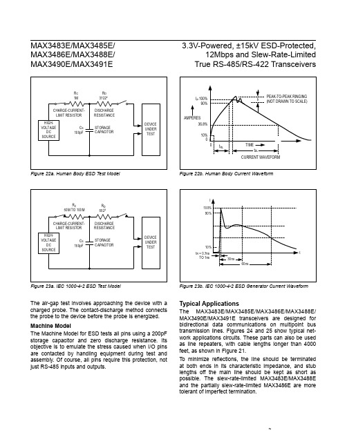
General DescriptionThe MAX481E, MAX483E, MAX485E, MAX487E–MAX491E, and MAX1487E are low-power transceivers for RS-485 and RS-422 communications in harsh environ-ments. Each driver output and receiver input is protected against ±15kV electro-static discharge (ESD) shocks,without latchup. These parts contain one driver and one receiver. The MAX483E, MAX487E, MAX488E, and MAX489E feature reduced slew-rate drivers that minimize EMI and reduce reflections caused by improperly termi-nated cables, thus allowing error-free data transmission up to 250kbps. The driver slew rates of the MAX481E,MAX485E, MAX490E, MAX491E, and MAX1487E are not limited, allowing them to transmit up to 2.5Mbps.These transceivers draw as little as 120µA supply cur-rent when unloaded or when fully loaded with disabled drivers (see Selector Guide ). Additionally, the MAX481E,MAX483E, and MAX487E have a low-current shutdown mode in which they consume only 0.5µA. All parts oper-ate from a single +5V supply.Drivers are short-circuit current limited, and are protected against excessive power dissipation by thermal shutdown circuitry that places their outputs into a high-impedance state. The receiver input has a fail-safe feature that guar-antees a logic-high output if the input is open circuit.The MAX487E and MAX1487E feature quarter-unit-load receiver input impedance, allowing up to 128 trans-ceivers on the bus. The MAX488E–MAX491E are designed for full-duplex communications, while the MAX481E, MAX483E, MAX485E, MAX487E, and MAX1487E are designed for half-duplex applications.For applications that are not ESD sensitive see the pin-and function-compatible MAX481, MAX483, MAX485,MAX487–MAX491, and MAX1487.ApplicationsLow-Power RS-485 Transceivers Low-Power RS-422 Transceivers Level TranslatorsTransceivers for EMI-Sensitive Applications Industrial-Control Local Area NetworksNext-Generation Device Features♦For Fault-Tolerant Applications:MAX3430: ±80V Fault-Protected, Fail-Safe, 1/4-Unit Load, +3.3V, RS-485 TransceiverMAX3080–MAX3089: Fail-Safe, High-Speed (10Mbps), Slew-Rate-Limited, RS-485/RS-422Transceivers ♦For Space-Constrained Applications:MAX3460–MAX3464: +5V, Fail-Safe, 20Mbps,Profibus, RS-485/RS-422 TransceiversMAX3362: +3.3V, High-Speed, RS-485/RS-422Transceiver in a SOT23 PackageMAX3280E–MAX3284E: ±15kV ESD-Protected,52Mbps, +3V to +5.5V, SOT23, RS-485/RS-422True Fail-Safe ReceiversMAX3030E–MAX3033E: ±15kV ESD-Protected,+3.3V, Quad RS-422 Transmitters ♦For Multiple Transceiver Applications:MAX3293/MAX3294/MAX3295: 20Mbps, +3.3V,SOT23, RS-485/RS-422 Transmitters ♦For Fail-Safe Applications:MAX3440E–MAX3444E: ±15kV ESD-Protected,±60V Fault-Protected, 10Mbps, Fail-Safe RS-485/J1708 Transceivers ♦For Low-Voltage Applications:MAX3483E/MAX3485E/MAX3486E/MAX3488E/MAX3490E/MAX3491E: +3.3V Powered, ±15kV ESD-Protected, 12Mbps, Slew-Rate-Limited, True RS-485/RS-422 TransceiversMAX481E/MAX483E/MAX485E/MAX487E–MAX491E/MAX1487E±15kV ESD-Protected, Slew-Rate-Limited, Low-Power, RS-485/RS-422 Transceivers________________________________________________________________Maxim Integrated Products 1Ordering Information19-0410; Rev 4; 10/03For pricing, delivery, and ordering information,please contact Maxim/Dallas Direct!at 1-888-629-4642, or visit Maxim’s website at .Ordering Information continued at end of data sheet.Selector Guide appears at end of data sheet .M A X 481E /M A X 483E /M A X 485E /M A X 487E –M A X 491E /M A X 1487E±15kV ESD-Protected, Slew-Rate-Limited,Low-Power, RS-485/RS-422 Transceivers2_______________________________________________________________________________________Supply Voltage (V CC ) (12V)Control Input Voltage (–R —E –, DE)...................-0.5V to (V CC + 0.5V)Driver Input Voltage (DI).............................-0.5V to (V CC + 0.5V)Driver Output Voltage (Y, Z; A, B)..........................-8V to +12.5V Receiver Input Voltage (A, B).................................-8V to +12.5V Receiver Output Voltage (RO)....................-0.5V to (V CC + 0.5V)Continuous Power Dissipation (T A = +70°C)8-Pin Plastic DIP (derate 9.09mW/°C above +70°C)....727mW14-Pin Plastic DIP (derate 10.00mW/°C above +70°C)..800mW 8-Pin SO (derate 5.88mW/°C above +70°C).................471mW 14-Pin SO (derate 8.33mW/°C above +70°C)...............667mW Operating Temperature RangesMAX4_ _C_ _/MAX1487EC_ A.............................0°C to +70°C MAX4__E_ _/MAX1487EE_ A...........................-40°C to +85°C Storage Temperature Range.............................-65°C to +160°C Lead Temperature (soldering, 10sec).............................+300°CDC ELECTRICAL CHARACTERISTICS(V CC = 5V ±5%, T A = T MIN to T MAX , unless otherwise noted.) (Notes 1, 2)Stresses beyond those listed under “Absolute Maximum Ratings” may cause permanent damage to the device. These are stress ratings only, and functional operation of the device at these or any other conditions beyond those indicated in the operational sections of the specifications is not implied. Exposure to absolute maximum rating conditions for extended periods may affect device reliability.ABSOLUTE MAXIMUM RATINGSPARAMETERSYMBOL MINTYPMAX UNITS Driver Common-Mode Output VoltageV OC 3V Change in Magnitude of Driver Differential Output Voltage for Complementary Output States ∆V OD 0.2V Change in Magnitude of Driver Common-Mode Output Voltage for Complementary Output States ∆V OD 0.2V Input High Voltage V IH 2.0V Input Low Voltage V IL 0.8V Input CurrentI IN1±2µADifferential Driver Output (no load)V OD15V 2V Differential Driver Output (with load)V OD2 1.551.0-0.8mA0.25mA -0.2Receiver Differential Threshold Voltage-0.20.2V Receiver Input Hysteresis ∆V TH 70mV Receiver Output High Voltage V OH 3.5Receiver Output Low Voltage V OL 0.4V Three-State (high impedance)Output Current at ReceiverI OZR±1µA 12k ΩCONDITIONSDE = 0V;V CC = 0V or 5.25V,all devices except MAX487E/MAX1487E R = 27Ωor 50Ω, Figure 8R = 27Ωor 50Ω, Figure 8R = 27Ωor 50Ω, Figure 8DE, DI, –R —E–MAX487E/MAX1487E,DE = 0V, V CC = 0V or 5.25VDE, DI, –R —E–DE, DI, –R —E–-7V ≤V CM ≤12V V CM = 0VI O = -4mA, V ID = 200mV I O = 4mA, V ID = -200mV R = 50Ω(RS-422)0.4V ≤V O ≤2.4VR = 27Ω(RS-485), Figure 8-7V ≤V CM ≤12V, all devices except MAX487E/MAX1487EReceiver Input Resistance R IN-7V ≤V CM ≤12V, MAX487E/MAX1487E48k ΩV TH I IN2Input Current (A, B)V IN = 12V V IN = -7V V IN = 12V V IN = -7VVMAX481E/MAX483E/MAX485E/MAX487E–MAX491E/MAX1487E±15kV ESD-Protected, Slew-Rate-Limited,Low-Power, RS-485/RS-422 TransceiversSWITCHING CHARACTERISTICS—MAX481E/MAX485E, MAX490E/MAX491E, MAX1487EDC ELECTRICAL CHARACTERISTICS (continued)(V CC = 5V ±5%, T A = T MIN to T MAX , unless otherwise noted.) (Notes 1, 2)M A X 481E /M A X 483E /M A X 485E /M A X 487E –M A X 491E /M A X 1487E±15kV ESD-Protected, Slew-Rate-Limited,Low-Power, RS-485/RS-422 Transceivers4_______________________________________________________________________________________SWITCHING CHARACTERISTICS—MAX483E, MAX487E/MAX488E/MAX489E(V CC = 5V ±5%, T A = T MIN to T MAX , unless otherwise noted.) (Notes 1, 2)SWITCHING CHARACTERISTICS—MAX481E/MAX485E, MAX490E/MAX491E, MAX1487E(continued)(V CC = 5V ±5%, T A = T MIN to T MAX , unless otherwise noted.) (Notes 1, 2)2251000Figures 11 and 13, C L = 100pF, S2 closed Figures 11 and 13, C L = 100pF, S1 closed Figures 9 and 15, C L = 15pF, S2 closed,A - B = 2VCONDITIONSns 45100t ZH(SHDN)Driver Enable from Shutdown toOutput High (MAX481E)nsFigures 9 and 15, C L = 15pF, S1 closed,B - A = 2Vt ZL(SHDN)Receiver Enable from Shutdownto Output Low (MAX481E)ns 45100t ZL(SHDN)Driver Enable from Shutdown toOutput Low (MAX481E)ns 2251000t ZH(SHDN)Receiver Enable from Shutdownto Output High (MAX481E)UNITS MINTYP MAX SYMBOLPARAMETERt PLH t SKEW Figures 10 and 12, R DIFF = 54Ω,C L1= C L2= 100pFt PHL Figures 10 and 12, R DIFF = 54Ω,C L1= C L2= 100pFDriver Input to Output Driver Output Skew to Output ns 20800ns ns 2000MAX483E/MAX487E, Figures 11 and 13,C L = 100pF, S2 closedt ZH(SHDN)Driver Enable from Shutdown to Output High2502000ns2500MAX483E/MAX487E, Figures 9 and 15,C L = 15pF, S1 closedt ZL(SHDN)Receiver Enable from Shutdown to Output Lowns 2500MAX483E/MAX487E, Figures 9 and 15,C L = 15pF, S2 closedt ZH(SHDN)Receiver Enable from Shutdown to Output Highns 2000MAX483E/MAX487E, Figures 11 and 13,C L = 100pF, S1 closedt ZL(SHDN)Driver Enable from Shutdown to Output Lowns 50200600MAX483E/MAX487E (Note 5)t SHDN Time to Shutdownt PHL t PLH , t PHL < 50% of data period Figures 9 and 15, C RL = 15pF, S2 closed Figures 9 and 15, C RL = 15pF, S1 closed Figures 9 and 15, C RL = 15pF, S2 closed Figures 9 and 15, C RL = 15pF, S1 closed Figures 11 and 13, C L = 15pF, S2 closed Figures 10 and 14, R DIFF = 54Ω,C L1= C L2= 100pFFigures 11 and 13, C L = 15pF, S1 closed Figures 11 and 13, C L = 100pF, S1 closed Figures 11 and 13, C L = 100pF, S2 closed CONDITIONSkbps 250f MAX 2508002000Maximum Data Rate ns 2550t HZ Receiver Disable Time from High ns 25080020002550t LZ Receiver Disable Time from Low ns 2550t ZH Receiver Enable to Output High ns 2550t ZL Receiver Enable to Output Low ns ns 1003003000t HZ t SKD Driver Disable Time from High I t PLH - t PHL I DifferentialReceiver SkewFigures 10 and 14, R DIFF = 54Ω,C L1= C L2= 100pFns 3003000t LZ Driver Disable Time from Low ns 2502000t ZL Driver Enable to Output Low ns Figures 10 and 12, R DIFF = 54Ω,C L1= C L2= 100pFns 2502000t R , t F 2502000Driver Rise or Fall Time ns t PLH Receiver Input to Output2502000t ZH Driver Enable to Output High UNITS MIN TYP MAX SYMBOL PARAMETERMAX481E/MAX483E/MAX485E/MAX487E–MAX491E/MAX1487E±15kV ESD-Protected, Slew-Rate-Limited,Low-Power, RS-485/RS-422 Transceivers_______________________________________________________________________________________505101520253035404550OUTPUT CURRENT vs.RECEIVER OUTPUT LOW VOLTAGEM A X 481E -01OUTPUT LOW VOLTAGE (V)O U T P U T C U R R E N T (m A )1.52.02.51.00.50.10.20.30.40.50.60.70.80.9-60-2060RECEIVER OUTPUT LOW VOLTAGEvs. TEMPERATURETEMPERATURE (°C)O U T P U T L O W V O L T A G E (V )20100-4040800-5-10-15-20-251.53.0OUTPUT CURRENT vs.RECEIVER OUTPUT HIGH VOLTAGEM A X 481E -02OUTPUT HIGH VOLTAGE (V)O U T P U T C U R R E N T (m A )5.04.54.02.02.53.53.03.23.43.63.84.04.24.44.64.8-60-2060RECEIVER OUTPUT HIGH VOLTAGEvs. TEMPERATURETEMPERATURE (°C)O U T P U T H I G H V O L T A G E (V )20100-4040800102030405060708090DRIVER OUTPUT CURRENT vs. DIFFERENTIAL OUTPUT VOLTAGEM A X 481E -05DIFFERENTIAL OUTPUT VOLTAGE (V)O U T P U T C U R R E N T (m A )1.52.0 2.53.0 3.54.0 4.51.00.50__________________________________________Typical Operating Characteristics(V CC = 5V, T A = +25°C, unless otherwise noted.)NOTES FOR ELECTRICAL/SWITCHING CHARACTERISTICSNote 1:All currents into device pins are positive; all currents out of device pins are negative. All voltages are referenced to deviceground unless otherwise specified.Note 2:All typical specifications are given for V CC = 5V and T A = +25°C.Note 3:Supply current specification is valid for loaded transmitters when DE = 0V.Note 4:Applies to peak current. See Typical Operating Characteristics.Note 5:The MAX481E/MAX483E/MAX487E are put into shutdown by bringing –R —E –high and DE low. If the inputs are in this state forless than 50ns, the parts are guaranteed not to enter shutdown. If the inputs are in this state for at least 600ns, the parts are guaranteed to have entered shutdown. See Low-Power Shutdown Mode section.M A X 481E /M A X 483E /M A X 485E /M A X 487E –M A X 491E /M A X 1487E±15kV ESD-Protected, Slew-Rate-Limited,Low-Power, RS-485/RS-422 Transceivers6___________________________________________________________________________________________________________________Typical Operating Characteristics (continued)(V CC = 5V, T A = +25°C, unless otherwise noted.)1.52.32.22.12.01.91.81.71.6-60-2060DRIVER DIFFERENTIAL OUTPUT VOLTAGE vs. TEMPERATURETEMPERATURE (°C)D I F FE R E N T I A L O U T P U T V O L T A G E (V )20100-404080020406080100120140OUTPUT CURRENT vs. DRIVER OUTPUT LOW VOLTAGEM A X 481E -07OUTPUT LOW VOLTAGE (V)O U T P U T C U R R E N T (m A )246810120-10-20-30-40-50-60-70-80-90-100-8-2OUTPUT CURRENT vs. DRIVER OUTPUT HIGH VOLTAGEM A X 481E -08OUTPUT HIGH VOLTAGE (V)O U T P U T C U R R E N T (m A )642-6-400100200300400500600-60-2060MAX481E/MAX485E/MAX490E/MAX491E SUPPLY CURRENT vs. TEMPERATURETEMPERATURE (°C)S U P P L Y C U R R E N T (µA )20100-4040800100200300400500600-60-2060MAX483E/MAX487E–MAX489E SUPPLY CURRENT vs. TEMPERATURETEMPERATURE (°C)S U P P L Y C U R R E N T (µA )20100-404080100200300400500600-60-2060MAX1487ESUPPLY CURRENT vs. TEMPERATURETEMPERATURE (°C)S U P P L Y C U R R E N T (µA )20100-404080±15kV ESD-Protected, Slew-Rate-Limited, Low-Power, RS-485/RS-422 Transceivers_______________________________________________________________________________________7MAX481E/MAX483E/MAX485E/MAX487E–MAX491E/MAX1487E______________________________________________________________Pin DescriptionM A X 481E /M A X 483E /M A X 485E /M A X 487E –M A X 491E /M A X 1487E±15kV ESD-Protected, Slew-Rate-Limited,Low-Power, RS-485/RS-422 Transceivers8_________________________________________________________________________________________________Function Tables (MAX481E/MAX483E/MAX485E/MAX487E/MAX1487E) Table 1. Transmitting__________Applications Information The MAX481E/MAX483E/MAX485E/MAX487E–MAX491E and MAX1487E are low-power transceivers for RS-485 and RS-422 communications. These “E” versions of the MAX481, MAX483, MAX485, MAX487–MAX491, and MAX1487 provide extra protection against ESD. The rugged MAX481E, MAX483E, MAX485E, MAX497E–MAX491E, and MAX1487E are intended for harsh envi-ronments where high-speed communication is important. These devices eliminate the need for transient suppres-sor diodes and the associated high capacitance loading. The standard (non-“E”) MAX481, MAX483, MAX485, MAX487–MAX491, and MAX1487 are recommended for applications where cost is critical.The MAX481E, MAX485E, MAX490E, MAX491E, and MAX1487E can transmit and receive at data rates up to 2.5Mbps, while the MAX483E, MAX487E, MAX488E, and MAX489E are specified for data rates up to 250kbps. The MAX488E–MAX491E are full-duplex transceivers, while the MAX481E, MAX483E, MAX487E, and MAX1487E are half-duplex. In addition, driver-enable (DE) and receiver-enable (RE) pins are included on the MAX481E, MAX483E, MAX485E, MAX487E, MAX489E, MAX491E, and MAX1487E. When disabled, the driver and receiver outputs are high impedance.±15kV ESD Protection As with all Maxim devices, ESD-protection structures are incorporated on all pins to protect against electro-static discharges encountered during handling and assembly. The driver outputs and receiver inputs have extra protection against static electricity. Maxim’s engi-neers developed state-of-the-art structures to protect these pins against ESD of ±15kV without damage. The ESD structures withstand high ESD in all states: normal operation, shutdown, and powered down. After an ESD event, Maxim’s MAX481E, MAX483E, MAX485E, MAX487E–MAX491E, and MAX1487E keep working without latchup.ESD protection can be tested in various ways; the transmitter outputs and receiver inputs of this product family are characterized for protection to ±15kV using the Human Body Model.Other ESD test methodologies include IEC10004-2 con-tact discharge and IEC1000-4-2 air-gap discharge (for-merly IEC801-2).ESD Test Conditions ESD performance depends on a variety of conditions. Contact Maxim for a reliability report that documents test set-up, test methodology, and test results.Human Body Model Figure 4 shows the Human Body Model, and Figure 5 shows the current waveform it generates when dis-charged into a low impedance. This model consists of a 100pF capacitor charged to the ESD voltage of inter-est, which is then discharged into the test device through a 1.5kΩresistor.IEC1000-4-2 The IEC1000-4-2 standard covers ESD testing and per-formance of finished equipment; it does not specifically refer to integrated circuits (Figure 6).MAX481E/MAX483E/MAX485E/MAX487E–MAX491E/MAX1487E±15kV ESD-Protected, Slew-Rate-Limited,Low-Power, RS-485/RS-422 Transceivers_______________________________________________________________________________________9M A X 481E /M A X 483E /M A X 485E /M A X 487E –M A X 491E /M A X 1487E±15kV ESD-Protected, Slew-Rate-Limited,Low-Power, RS-485/RS-422 Transceivers10______________________________________________________________________________________Figure 8. Driver DC Test LoadFigure 9. Receiver Timing Test LoadMAX481E/MAX483E/MAX485E/MAX487E–MAX491E/MAX1487E±15kV ESD-Protected, Slew-Rate-Limited,Low-Power, RS-485/RS-422 Transceivers______________________________________________________________________________________11Figure 10. Driver/Receiver Timing Test Circuit Figure 11. Driver Timing Test LoadFigure 12. Driver Propagation DelaysFigure 13. Driver Enable and Disable Times (except MAX488E and MAX490E)Figure 14. Receiver Propagation DelaysFigure 15. Receiver Enable and Disable Times (except MAX488E and MAX490E)M A X 481E /M A X 483E /M A X 485E /M A X 487E –M A X 491E /M A X 1487E±15kV ESD-Protected, Slew-Rate-Limited,Low-Power, RS-485/RS-422 Transceivers12______________________________________________________________________________________The major difference between tests done using the Human Body Model and IEC1000-4-2 is higher peak current in IEC1000-4-2, because series resistance is lower in the IEC1000-4-2 model. Hence, the ESD with-stand voltage measured to IEC1000-4-2 is generally lower than that measured using the Human Body Model. Figure 7 shows the current waveform for the 8kV IEC1000-4-2 ESD contact-discharge test.The air-gap test involves approaching the device with a charged probe. The contact-discharge method connects the probe to the device before the probe is energized.Machine ModelThe Machine Model for ESD tests all pins using a 200pF storage capacitor and zero discharge resis-tance. Its objective is to emulate the stress caused by contact that occurs with handling and assembly during manufacturing. Of course, all pins require this protec-tion during manufacturing—not just inputs and outputs.Therefore,after PC board assembly,the Machine Model is less relevant to I/O ports.MAX487E/MAX1487E:128 Transceivers on the BusThe 48k Ω, 1/4-unit-load receiver input impedance of the MAX487E and MAX1487E allows up to 128 transceivers on a bus, compared to the 1-unit load (12k Ωinput impedance) of standard RS-485 drivers (32 transceivers maximum). Any combination of MAX487E/MAX1487E and other RS-485 transceivers with a total of 32 unit loads or less can be put on the bus. The MAX481E,MAX483E, MAX485E, and MAX488E–MAX491E have standard 12k Ωreceiver input impedance.MAX483E/MAX487E/MAX488E/MAX489E:Reduced EMI and Reflections The MAX483E and MAX487E–MAX489E are slew-rate limited, minimizing EMI and reducing reflections caused by improperly terminated cables. Figure 16shows the driver output waveform and its Fourier analy-sis of a 150kHz signal transmitted by a MAX481E,MAX485E, MAX490E, MAX491E, or MAX1487E. High-frequency harmonics with large amplitudes are evident.Figure 17 shows the same information displayed for a MAX483E, MAX487E, MAX488E, or MAX489E transmit-ting under the same conditions. Figure 17’s high-fre-quency harmonics have much lower amplitudes, and the potential for EMI is significantly reduced.Low-Power Shutdown Mode (MAX481E/MAX483E/MAX487E)A low-power shutdown mode is initiated by bringing both RE high and DE low. The devices will not shut down unless both the driver and receiver are disabled.In shutdown, the devices typically draw only 0.5µA of supply current.RE and DE may be driven simultaneously; the parts are guaranteed not to enter shutdown if RE is high and DE is low for less than 50ns. If the inputs are in this state for at least 600ns, the parts are guaranteed to enter shutdown.For the MAX481E, MAX483E, and MAX487E, the t ZH and t ZL enable times assume the part was not in the low-power shutdown state (the MAX485E, MAX488E–MAX491E, and MAX1487E can not be shut down). The t ZH(SHDN)and t ZL(SHDN)enable times assume the parts were shut down (see Electrical Characteristics ).500kHz/div0Hz5MHz 10dB/div Figure 16. Driver Output Waveform and FFT Plot ofMAX485E/MAX490E/MAX491E/MAX1487E Transmitting a 150kHz Signal500kHz/div0Hz5MHz10dB/divFigure 17. Driver Output Waveform and FFT Plot ofMAX483E/MAX487E–MAX489E Transmitting a 150kHz SignalIt takes the drivers and receivers longer to become enabled from the low-power shutdown state (t ZH(SHDN), t ZL(SHDN)) than from the operating mode (t ZH, t ZL). (The parts are in operating mode if the RE, DE inputs equal a logical 0,1 or 1,1 or 0, 0.)Driver Output Protection Excessive output current and power dissipation caused by faults or by bus contention are prevented by two mechanisms. A foldback current limit on the output stage provides immediate protection against short circuits over the whole common-mode voltage range (see Typical Operating Characteristics). In addition, a thermal shut-down circuit forces the driver outputs into a high-imped-ance state if the die temperature rises excessively.Propagation Delay Many digital encoding schemes depend on the differ-ence between the driver and receiver propagation delay times. Typical propagation delays are shown in Figures 19–22 using Figure 18’s test circuit.The difference in receiver delay times, t PLH- t PHL, is typically under 13ns for the MAX481E, MAX485E, MAX490E, MAX491E, and MAX1487E, and is typically less than 100ns for the MAX483E and MAX487E–MAX489E.The driver skew times are typically 5ns (10ns max) for the MAX481E, MAX485E, MAX490E, MAX491E, and MAX1487E, and are typically 100ns (800ns max) for the MAX483E and MAX487E–MAX489E.Typical Applications The MAX481E, MAX483E, MAX485E, MAX487E–MAX491E, and MAX1487E transceivers are designed for bidirectional data communications on multipoint bus transmission lines. Figures 25 and 26 show typical net-work application circuits. These parts can also be used as line repeaters, with cable lengths longer than 4000 feet. To minimize reflections, the line should be terminated at both ends in its characteristic impedance, and stub lengths off the main line should be kept as short as possi-ble. The slew-rate-limited MAX483E and MAX487E–MAX489E are more tolerant of imperfect termination. Bypass the V CC pin with 0.1µF.Isolated RS-485 For isolated RS-485 applications, see the MAX253 and MAX1480 data sheets.Line Length vs. Data Rate The RS-485/RS-422 standard covers line lengths up to 4000 feet. Figures 23 and 24 show the system differen-tial voltage for the parts driving 4000 feet of 26AWG twisted-pair wire at 110kHz into 100Ωloads.Figure 18. Receiver Propagation Delay Test CircuitMAX481E/MAX483E/MAX485E/MAX487E–MAX491E/MAX1487E±15kV ESD-Protected, Slew-Rate-Limited,Low-Power, RS-485/RS-422 Transceivers ______________________________________________________________________________________13M A X 481E /M A X 483E /M A X 485E /M A X 487E –M A X 491E /M A X 1487E±15kV ESD-Protected, Slew-Rate-Limited,Low-Power, RS-485/RS-422 Transceivers14______________________________________________________________________________________25ns/div 5V/divRO B A500mV/div Figure 19. MAX481E/MAX485E/MAX490E/MAX1487E Receiver t PHL25ns/div5V/div ROBA500mV/divFigure 20. MAX481E/MAX485E/MAX490E/MAX491E/MAX1487E Receiver t PLH200ns/div 5V/divRO B A500mV/div Figure 21. MAX483E/MAX487E–MAX489E Receiver t PHL200ns/div5V/div ROBA500mV/divFigure 22. MAX483E/MAX487E–MAX489E Receiver t PLH2µs/div DO 0V0V5V5V -1V 0DIV A - V BFigure 23. MAX481E/MAX485E/MAX490E/MAX491E/MAX1487E System Differential Voltage at 110kHz Driving 4000ft of Cable 2µs/divDO0V0V 5V 5V -1V1V0DIV B - V AFigure 24. MAX483E/MAX1487E–MAX489E System Differential Voltage at 110kHz Driving 4000ft of CableMAX481E/MAX483E/MAX485E/MAX487E–MAX491E/MAX1487E±15kV ESD-Protected, Slew-Rate-Limited,Low-Power, RS-485/RS-422 Transceivers______________________________________________________________________________________15Figure 26. MAX488E–MAX491E Full-Duplex RS-485 NetworkFigure 25. MAX481E/MAX483E/MAX485E/MAX487E/MAX1487E Typical Half-Duplex RS-485 NetworkM A X 481E /M A X 483E /M A X 485E /M A X 487E –M A X 491E /M A X 1487E±15kV ESD-Protected, Slew-Rate-Limited, Low-Power, RS-485/RS-422 Transceivers Maxim cannot assume responsibility for use of any circuitry other than circuitry entirely embodied in a Maxim product. No circuit patent licenses are implied. Maxim reserves the right to change the circuitry and specifications without notice at any time.16____________________Maxim Integrated Products, 120 San Gabriel Drive, Sunnyvale, CA 94086 408-737-7600©2003 Maxim Integrated ProductsPrinted USAis a registered trademark of Maxim Integrated Products.Package InformationFor the latest package outline information, go to /packages .Ordering Information (continued)Selector GuideChip InformationTRANSISTOR COUNT: 295。
max3485esa中文资料
General Description The MAX3483, MAX3485, MAX3486, MAX3488,MAX3490, and MAX3491 are 3.3V , low-power transceivers forRS-485 and RS-422 communication. Each part containsone driver and one receiver. The MAX3483 and MAX3488feature slew-rate-limited drivers that minimize EMI andreduce reflections caused by improperly terminatedcables, allowing error-free data transmission at data ratesup to 250kbps. The partially slew-rate-limited MAX3486transmits up to 2.5Mbps. The MAX3485, MAX3490, andMAX3491 transmit at up to 10Mbps.Drivers are short-circuit current-limited and are protectedagainst excessive power dissipation by thermal shutdowncircuitry that places the driver outputs into a high-imped-ance state. The receiver input has a fail-safe feature thatguarantees a logic-high output if both inputs are opencircuit.The MAX3488, MAX3490, and MAX3491 feature full-duplex communication, while the MAX3483, MAX3485, andMAX3486 are designed for half-duplex communication.Applications ●Low-Power RS-485/RS-422 Transceivers ●Telecommunications ●Transceivers for EMI-Sensitive Applications ●Industrial-Control Local Area NetworksFeatures●Operate from a Single 3.3V Supply—No Charge Pump!●Interoperable with +5V Logic ●8ns Max Skew (MAX3485/MAX3490/MAX3491)●Slew-Rate Limited for Errorless Data Transmission (MAX3483/MAX3488)●2nA Low-Current Shutdown Mode (MAX3483/MAX3485/MAX3486/MAX3491)●-7V to +12V Common-Mode Input Voltage Range ●Allows up to 32 Transceivers on the Bus ●Full-Duplex and Half-Duplex Versions Available ●Industry Standard 75176 Pinout (MAX3483/MAX3485/MAX3486)●Current-Limiting and Thermal Shutdown for Driver Overload Protection 19-0333; Rev 1; 5/19Ordering Information continued at end of data sheet.*Contact factory for for dice specifications.PARTTEMP . RANGE PIN-PACKAGE MAX3483CPA0°C to +70°C 8 Plastic DIP MAX3483CSA0°C to +70°C 8 SO MAX3483C/D0°C to +70°C Dice*MAX3483EPA-40°C to +85°C 8 Plastic DIP MAX3483ESA-40°C to +85°C 8 SO MAX3485CPA0°C to +70°C 8 Plastic DIP MAX3485CSA0°C to +70°C 8 SO MAX3485C/D0°C to +70°C Dice*MAX3485EPA-40°C to +85°C 8 Plastic DIP MAX3485ESA -40°C to +85°C 8 SO PARTNUMBERGUARANTEED DATA RATE (Mbps)SUPPLY VOLTAGE (V)HALF/FULL DUPLEX SLEW-RATE LIMITED DRIVER/RECEIVER ENABLE SHUTDOWN CURRENT (nA)PIN COUNT MAX34830.25 3.0 to 3.6Half Yes Yes 28MAX348510Half No No 28MAX34862.5Half Yes Yes 28MAX34880.25Half Yes Yes —8MAX349010Half No No —8MAX349110Half No Yes 214MAX3483/MAX3485/MAX3486/MAX3488/MAX3490/MAX3491Selection TableOrdering Information找电子元器件上宇航军工Figure 1. MAX3483/MAX3485/MAX3486 Pin Configuration and Typical Operating Circuit Figure 2. MAX3488/MAX3490 Pin Configuration and Typical Operating Circuit Figure 3. MAX3491 Pin Configuration and Typical Operating CircuitMAX3486/MAX3488/MAX3490/MAX3491True RS-485/RS-422 TransceiversFigure 22. MAX3488/MAX3490/MAX3491 Full-Duplex RS-485 NetworkFigure 23. Line Repeater for MAX3488/MAX3490/MAX3491MAX3486/MAX3488/MAX3490/MAX3491True RS-485/RS-422 Transceivers。
max3485中文资料

max3485中文资料max3485eesa + T概述Max3485eesa + T是3.3V电源±15kV ESD保护,真正的RS485 / RS422收发器,采用8引脚nsoic封装。
该低功耗收发器包含一个驱动器和一个接收器。
max3485e传输速率高达15Mbps。
它具有增强的静电保护。
所有发送器输出和接收器输入均具有±15kV保护,并通过IEC 1000-4-2气隙放电;±8Kv保护是通过IEC 1000-4-2接触放电,±15kV保护是通过人体模型。
驱动器受到短路电流的限制,并通过将驱动器输出置于高阻抗状态的热关断电路来防止过多的功耗。
接收器输入具有故障安全功能,如果两个输入均打开,则提供逻辑高电平输出。
Max3485e适用于EMI敏感应用,集成服务,数字网络和数据包交换电源电压范围:3V至3.6V工作温度范围-40°C至85°C半双工通讯该操作由单个+ 3.3V电源供电,无电荷泵兼容+ 5V逻辑2Na小电流关闭模式共模输入电压范围:-7V至+ 12V工业标准75176引脚输出驱动器/接收器启用功能工业控制LAN,ISDN,低功耗RS-485 / RS-422收发器;分组交换;电信;用于EMI敏感应用的收发器Max3483,max3485,max3486,max3488,max3490和max3491是用于RS-485和RS-422通信的3.3V低功耗收发器,每个收发器都有一个驱动器和一个接收器。
Max3483和max3488具有有限速率驱动器,可以降低EMI并减少由于端子匹配电缆不合适而引起的反射,从而实现高达250kbps的无错误数据传输。
由于其有限的摆幅速率,Max3486可以实现最大2.5mbps 的传输速率。
Max3485,max3490和max3491可以实现高达10Mbps的传输速率。
驱动器具有短路电流限制,并且可以通过热关断电路将驱动器的输出设置为高阻状态,以防止过多的功率损耗。
MEMORY存储芯片MAX3483EPA中文规格书
Typical Applications The MAX3483E/MAX3485E/MAX3486E/MAX3488E/MAX3490E/MAX3491E transceivers are designed for bidirectional data communications on multipoint bus transmission lines. Figures 24 and 25 show typical net-work applications circuits. These parts can also be used as line repeaters, with cable lengths longer than 4000 feet, as shown in Figure 21.To minimize reflections, the line should be terminated at both ends in its characteristic impedance, and stublengths off the main line should be kept as short as possible. The slew-rate-limited MAX3483E/MAX3488E and the partially slew-rate-limited MAX3486E are more tolerant of imperfect termination.Figure 22a. Human Body ESD Test ModelFigure 22b. Human Body Current Waveform Figure 23b. IEC 1000-4-2 ESD Generator Current WaveformFigure 23a. IEC 1000-4-2 ESD Test ModelThe air-gap test involves approaching the device with a charged probe. The contact-discharge method connects the probe to the device before the probe is energized.Machine ModelThe Machine Model for ESD tests all pins using a 200pF storage capacitor and zero discharge resistance. Its objective is to emulate the stress caused when I/O pins are contacted by handling equipment during test and assembly. Of course, all pins require this protection, not just RS-485 inputs and outputs.~MAX3483E/MAX3485E/MAX3486E/MAX3488E/MAX3490E/MAX3491E3.3V-Powered, ±15kV ESD-Protected, 12Mbps and Slew-Rate-Limited True RS-485/RS-422 TransceiversFigure 24. MAX3483E/MAX3485E/MAX3486E Typical RS-485 NetworkFigure 25. MAX3488E/MAX3490E/MAX3491E Full-Duplex RS-485 NetworkMAX3483E/MAX3485E/MAX3486E/MAX3488E/MAX3490E/MAX3491E3.3V-Powered, ±15kV ESD-Protected, 12Mbps and Slew-Rate-Limited True RS-485/RS-422 Transceivers。
max3485中文资料
MAX3483, MAX3485, MAX3486, MAX3488, MAX3490以及MAX3491是用于RS-485与RS-422通信的3.3V,低功耗收发器,每个器件中都具有一个驱动器和一个接收器。
MAX3483和MAX3488具有限摆率驱动器,可以减小EMI,并降低由不恰当的终端匹配电缆引起的反射,实现最高250kbps的无差错数据传输。
MAX3486的驱动器摆率部分受限,可以实现最高2.5Mbps的传输速率。
MAX3485,MAX3490和MAX3491则可以实现最高10Mbps 的传输速率。
驱动器具有短路电流限制,并可以通过热关断电路将驱动器输出置为高阻状态,防止过度的功率损耗。
接收器输入具有失效保护特性,当输入开路时,可以确保逻辑高电平输出。
使用MAX3488, MAX3490和MAX3491可以实现全双工通信,而MAX3483,MAX3485与MAX3486则为半双工应用设计。
这篇文章介绍的就是MAX34852 芯片介绍2.1 主要特点半双工速率:10Mbps限摆率:NO接收允许控制:YES 关断电流:2 nA引脚数:82.2 引脚配置根据上图、上表可知:DE和RO为使能管脚。
DE为低电平、RE为低电平时为接收;DE 为高电平、RE为高电平时为发送;RO和DI为数据管脚。
RO为接收,DI为发送;因此我们经常将DE和RE直接连接,用一个IO口控制(见3.2 电路实现)。
3.1 应用场景工业控制局域网集成服务数字网络低功耗RS-485/RS-422收发器(我做的几个项目都是该功能)分组交换技术电信用于EMI敏感应用的收发器3.2 电路实现485是2线式,两个485接口的设备相连通过A、B两根线即可(也就是至少2个485芯片),连接方式如下图所示:我们使用MAX3485一般是用下图电路:从上图中我们可以看到:RO直接和TTL电平的UART_RX(或模拟串口的RX)相连,DI直接和TTL电平的UART_TX(或模拟串口的TX)相连,R34为1K。
MEMORY存储芯片MAX1487EPA+中文规格书

General DescriptionThe MAX481, MAX483, MAX485, MAX487–MAX491, andMAX1487 are low-power transceivers for RS-485 and RS-422 communication. Each part contains one driver and onereceiver. The MAX483, MAX487, MAX488, and MAX489feature reduced slew-rate drivers that minimize E MI andreduce reflections caused by improperly terminated cables,thus allowing error-free data transmission up to 250kbps.The driver slew rates of the MAX481, MAX485, MAX490,MAX491, and MAX1487 are not limited, allowing them totransmit up to 2.5Mbps.These transceivers draw between 120µA and 500µA ofsupply current when unloaded or fully loaded with disableddrivers. Additionally, the MAX481, MAX483, and MAX487have a low-current shutdown mode in which they consumeonly 0.1µA. All parts operate from a single 5V supply.Drivers are short-circuit current limited and are protectedagainst excessive power dissipation by thermal shutdowncircuitry that places the driver outputs into a high-imped-ance state. The receiver input has a fail-safe feature thatguarantees a logic-high output if the input is open circuit.The MAX487 and MAX1487 feature quarter-unit-loadreceiver input impedance, allowing up to 128 MAX487/MAX1487 transceivers on the bus. Full-duplex communi-cations are obtained using the MAX488–MAX491, whilethe MAX481, MAX483, MAX485, MAX487, and MAX1487are designed for half-duplex applications.________________________Applications Low-Power RS-485 Transceivers Low-Power RS-422 Transceivers Level Translators Transceivers for EMI-Sensitive Applications Industrial-Control Local Area Networks__Next Generation Device Features o For Fault-Tolerant Applications MAX3430: ±80V Fault-Protected, Fail-Safe, 1/4Unit Load, +3.3V, RS-485 Transceiver MAX3440E–MAX3444E: ±15kV ESD-Protected,±60V Fault-Protected, 10Mbps, Fail-Safe, RS-485/J1708 Transceivers o For Space-Constrained Applications MAX3460–MAX3464: +5V, Fail-Safe, 20Mbps,Profibus RS-485/RS-422 Transceivers MAX3362: +3.3V, High-Speed, RS-485/RS-422Transceiver in a SOT23 Package MAX3280E–MAX3284E: ±15kV ESD-Protected,52Mbps, +3V to +5.5V, SOT23, RS-485/RS-422,True Fail-Safe Receivers MAX3293/MAX3294/MAX3295: 20Mbps, +3.3V,SOT23, RS-485/RS-422 Transmitters o For Multiple Transceiver Applications MAX3030E–MAX3033E: ±15kV ESD-Protected,+3.3V, Quad RS-422 Transmitters o For Fail-Safe Applications MAX3080–MAX3089: Fail-Safe, High-Speed (10Mbps), Slew-Rate-Limited RS-485/RS-422Transceiverso For Low-Voltage ApplicationsMAX3483E/MAX3485E/MAX3486E/MAX3488E/MAX3490E/MAX3491E: +3.3V Powered, ±15kVESD-Protected, 12Mbps, Slew-Rate-Limited,True RS-485/RS-422 Transceivers For pricing, delivery, and ordering information, please contact Maxim Direct at 1-,or visit Maxim Integrated’s website at .______________________________________________________________Selection Table19-0122; Rev 10; 9/14PARTNUMBERHALF/FULL DUPLEX DATA RATE (Mbps) SLEW-RATE LIMITED LOW-POWER SHUTDOWN RECEIVER/DRIVER ENABLE QUIESCENT CURRENT (μA) NUMBER OF RECEIVERS ON BUS PIN COUNT MAX481Half 2.5No Yes Yes 300328MAX483Half 0.25Yes Yes Yes 120328MAX485Half 2.5No No Yes 300328MAX487Half 0.25Yes Yes Yes 1201288MAX488Full 0.25Yes No No 120328MAX489Full 0.25Yes No Yes 1203214MAX490Full 2.5No No No 300328MAX491Full 2.5No No Yes 3003214MAX1487 Half 2.5No No Yes 2301288Ordering Information appears at end of data sheet.找MEMORY 、二三极管上美光存储Low-Power, Slew-Rate-Limited RS-485/RS-422 Transceivers 8Maxim Integrated MAX481/MAX483/MAX485/MAX487–MAX491/MAX1487__________Applications Information The MAX481/MAX483/MAX485/MAX487–MAX491 and MAX1487 are low-power transceivers for RS-485 and RS-422 communications. The MAX481, MAX485, MAX490,MAX491, and MAX1487 can transmit and receive at data rates up to 2.5Mbps, while the MAX483, MAX487,MAX488, and MAX489 are specified for data rates up to 250kbps. The MAX488–MAX491 are full-duplex trans-ceivers while the MAX481, MAX483, MAX485, MAX487,and MAX1487 are half-duplex. In addition, Driver Enable (DE) and Receiver Enable (RE ) pins are included on the MAX481, MAX483, MAX485, MAX487, MAX489,MAX491, and MAX1487. When disabled, the driver and receiver outputs are high impedance.MAX487/MAX1487:128 Transceivers on the Bus The 48k Ω, 1/4-unit-load receiver input impedance of the MAX487 and MAX1487 allows up to 128 transceivers on a bus, compared to the 1-unit load (12k Ωinput impedance) of standard RS-485 drivers (32 trans-ceivers maximum). Any combination of MAX487/MAX1487 and other RS-485 transceivers with a total of 32 unit loads or less can be put on the bus. The MAX481/MAX483/MAX485 and MAX488–MAX491 have standard 12k ΩReceiver Input impedance.Figure 2. MAX488/MAX490 Pin Configuration and Typical Operating Circuit Figure 3. MAX489/MAX491 Pin Configuration and Typical Operating Circuit。
MAX490EEPA中文资料
元器件交易网
MAX481E/MAX483E/MAX485E/MAX487E–MAX491E/MAX1487E
19-0410; Rev 4; 10/03
±15kV ESD-Protected, Slew-Rate-Limited, Low-Power, RS-485/RS-422 Transceivers
Ordering Information
PART MAX481ECPA MAX481ECSA MAX481EEPA MAX481EESA MAX483ECPA MAX483ECSA MAX483EEPA MAX483EESA
TEMP RANGE 0°C to +70°C 0°C to +70°C -40°C to +85°C -40°C to +85°C 0°C to +70°C 0°C to +70°C -40°C to +85°C -40°C to +85°C
- 1、下载文档前请自行甄别文档内容的完整性,平台不提供额外的编辑、内容补充、找答案等附加服务。
- 2、"仅部分预览"的文档,不可在线预览部分如存在完整性等问题,可反馈申请退款(可完整预览的文档不适用该条件!)。
- 3、如文档侵犯您的权益,请联系客服反馈,我们会尽快为您处理(人工客服工作时间:9:00-18:30)。
元器件交易网
3.3V-Powered, 10Mbps and Slew-Rate-Limited True RS-485/RS-422 Transceivers
MAX3483/MAX3485/MAX3486/MAX3488/MAX3490/MAX3491
ABSOLUTE MAXIMUM RATINGS
元器件交易网
19-0333;ቤተ መጻሕፍቲ ባይዱRev 0; 12/94
3.3V-Powered, 10Mbps and Slew-Rate-Limited True RS-485/RS-422 Transceivers
_______________General Description
The MAX3483, MAX3485, MAX3486, MAX3488, MAX3490, and MAX3491 are 3.3V, low-power transceivers for RS-485 and RS-422 communication. Each part contains one driver and one receiver. The MAX3483 and MAX3488 feature slew-rate-limited drivers that minimize EMI and reduce reflections caused by improperly terminated cables, allowing error-free data transmission at data rates up to 250kbps. The partially slew-rate-limited MAX3486 transmits up to 2.5Mbps. The MAX3485, MAX3490, and MAX3491 transmit at up to 10Mbps. Drivers are short-circuit current limited and are protected against excessive power dissipation by thermal shutdown circuitry that places the driver outputs into a high-impedance state. The receiver input has a fail-safe feature that guarantees a logic-high output if both inputs are open circuit. The MAX3488, MAX3490, and MAX3491 feature fullduplex communication, while the MAX3483, MAX3485, and MAX3486 are designed for half-duplex communication.
PART NUMBER MAX3483 MAX3485 MAX3486 MAX3488 MAX3490 MAX3491 GUARANTEED DATA RATE (Mbps) 0.25 10 2.5 0.25 10 10 3.0 to 3.6 SUPPLY VOLTAGE (V) HALF/FULL DUPLEX Half Half Half Full Full Full SLEW-RATE LIMITED Yes No Yes Yes No No DRIVER/ RECEIVER ENABLE Yes Yes Yes No No Yes SHUTDOWN CURRENT (nA) 2 2 2 — — 2 PIN COUNT 8 8 8 8 8 14 1
____________________________Features
o Operate from a Single 3.3V Supply— No Charge Pump! o Interoperable with +5V Logic o 8ns Max Skew (MAX3485/MAX3490/MAX3491) o Slew-Rate Limited for Errorless Data Transmission (MAX3483/MAX3488) o 2nA Low-Current Shutdown Mode (MAX3483/MAX3485/MAX3486/MAX3491) o -7V to +12V Common-Mode Input Voltage Range o Allows up to 32 Transceivers on the Bus o Full-Duplex and Half-Duplex Versions Available o Industry Standard 75176 Pinout (MAX3483/MAX3485/MAX3486) o Current-Limiting and Thermal Shutdown for Driver Overload Protection
DC ELECTRICAL CHARACTERISTICS
(VCC = 3.3V ±0.3V, TA = TMIN to TMAX, unless otherwise noted. Typical values are at TA = +25°C) PARAMETER Differential Driver Output Change in Magnitude of Driver Differential Output Voltage for Complementary Output States (Note 1) Driver Common-Mode Output Voltage Change in Magnitude of Common-Mode Output Voltage (Note 1) Input High Voltage Input Low Voltage Logic Input Current Input Current (A, B) Output Leakage (Y, Z) Output Leakage (Y, Z) in Shutdown Mode Receiver Differential Threshold Voltage Receiver Input Hysteresis Receiver Output High Voltage Receiver Output Low Voltage Three-State (High Impedance) Output Current at Receiver Receiver Input Resistance SYMBOL VOD CONDITIONS RL = 100Ω (RS-422), Figure 4 RL = 54Ω (RS-485), Figure 4 RL = 60Ω (RS-485), VCC = 3.3V, Figure 5 ∆VOD RL = 54Ω or 100Ω, Figure 4 MIN 2.0 1.5 1.5 V TYP MAX UNITS
Stresses beyond those listed under “Absolute Maximum Ratings” may cause permanent damage to the device. These are stress ratings only, and functional operation of the device at these or any other conditions beyond those indicated in the operational sections of the specifications is not implied. Exposure to absolute maximum rating conditions for extended periods may affect device reliability.
________________________Applications
Low-Power RS-485/RS-422 Transceivers Telecommunications Transceivers for EMI-Sensitive Applications Industrial-Control Local Area Networks
Ordering Information continued at end of data sheet. * Contact factory for for dice specifications.
______________________________________________________________Selection Table
MAX3483/MAX3485/MAX3486/MAX3488/MAX3490/MAX3491
______________Ordering Information
PART MAX3483CPA MAX3483CSA MAX3483C/D MAX3483EPA MAX3483ESA MAX3485CPA MAX3485CSA MAX3485C/D MAX3485EPA MAX3485ESA TEMP. RANGE 0°C to +70°C 0°C to +70°C 0°C to +70°C -40°C to +85°C -40°C to +85°C 0°C to +70°C 0°C to +70°C 0°C to +70°C -40°C to +85°C -40°C to +85°C PIN-PACKAGE 8 Plastic DIP 8 SO Dice* 8 Plastic DIP 8 SO 8 Plastic DIP 8 SO Dice* 8 Plastic DIP 8 SO
________________________________________________________________ Maxim Integrated Products