cmos4046集成电路研究锁相环(pll)的工作原理毕业外文翻译
锁相环PLL(PhaseLockedLoop)
锁相环PLL(PhaseLockedLoop)锁相环PLL目前我见到的所有芯片中都含有PLL模块,而且一直不知道如何利用PLL对晶振进行倍频的,这次利用维基百科好好的学习了下PLL 的原理。
1. 时钟与振荡电路在芯片中,最重要的就是时钟,时钟就像是心脏的脉冲,如果心脏停止了跳动,那人也就死亡了,对于芯片也一样。
了解了时钟的重要性,那时钟是怎么来的呢?时钟可以看成周期性的0与1信号变化,而这种周期性的变化可以看成振荡。
因此,振荡电路成为了时钟的来源。
振荡电路的形成可以分两类:1. 石英晶体的压电效应:电导致晶片的机械变形,而晶片两侧施加机械压力又会产生电,形成振荡。
它的谐振频率与晶片的切割方式、几何形状、尺寸有关,可以做得精确,因此其振荡电路可以获得很高的频率稳定度。
2. 电容Capacity的充电放电:能够存储电能,而充放电的电流方向是反的,形成振荡。
可通过电压等控制振荡电路的频率。
2. PLL与倍频由上面可以知道,晶振由于其频率的稳定性,一般作为系统的外部时钟源。
但是晶振的频率虽然稳定,但是频率无法做到很高(成本与工艺限制),因此芯片中高频时钟就需要一种叫做压控振荡器(Voltage Controlled Oscillator)的东西生成了(顾名思义,VCO 就是根据电压来调整输出频率的不同)。
可压控振荡器也有问题,其频率不够稳定,而且变化时很难快速稳定频率。
哇偶,看到这种现象是不是很熟悉?嘿嘿,这就是标准开环系统所出现的问题,解决办法就是接入反馈,使开环系统变成闭环系统,并且加入稳定的基准信号,与反馈比较,以便生成正确的控制。
PLL倍频电路因此,为了将频率锁定在一个固定的期望值,锁相环PLL出现了!一个锁相环PLL电路通常由以下模块组成:·鉴相鉴频器PFD(Phase Frequency Detector):对输入的基准信号(来自频率稳定的晶振)和反馈回路的信号进行频率的比较,输出一个代表两者差异的信号·低通滤波器LPF(Low-Pass Filter):将PFD中生成的差异信号的高频成分滤除,保留直流部分·压控振荡器VCO(Voltage Controlled Oscillator):根据输入电压,输出对应频率的周期信号。
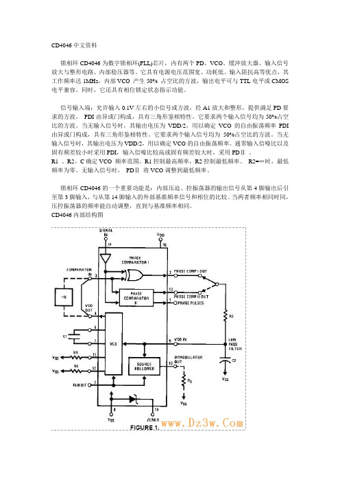
cd4046中文资料
CD4046是通用的CMOS锁相环集成电路,其特点是电源电压范围宽(为3V-18V),输入阻抗高(约100MΩ),动态功耗小,在中心频率f0为10kHz下功耗仅为600μW,属微功耗器件。
CD4046锁相的意义是相位同步的自动控制,功能是完成两个电信号相位同步的自动控制闭环系统叫做锁相环,简称PLL。
它广泛应用于广播通信、频率合成、自动控制及时钟同步等技术领域。
锁相环主要由相位比较器(PC)、压控振荡器(VCO)。
低通滤波器三部分组成,如下所示。
〈CD4046内部电原理框图〉CD4046工作原理:输入信号Ui从14脚输入后,经放大器A1进行放大、整形后加到相位比较器Ⅰ、Ⅱ的输入端,图3开关K拨至2脚,则比较器Ⅰ将从3脚输入的比较信号Uo与输入信号Ui作相位比较,从相位比较器输出的误差电压UΨ则反映出两者的相位差。
UΨ经R3、R4及C2滤波后得到一控制电压Ud加至压控振荡器VCO的输入端9脚,调整VCO的振荡频率f2,使f 2迅速逼近信号频率f1。
VCO的输出又经除法器再进入相位比较器Ⅰ,继续与Ui进行相位比较,最后使得f2=f1,两者的相位差为一定值,实现了相位锁定。
若开关K拨至13脚,则相位比较器Ⅱ工作,过程与上述相同,不再赘述。
下图是CD4046的引脚排列,采用16脚双列直插式,各管脚功能:1脚相位输出端,环路人锁时为高电平,环路失锁时为低电平。
2脚相位比较器Ⅰ的输出端。
3脚比较信号输入端。
4脚压控振荡器输出端。
5脚禁止端,高电平时禁止,低电平时允许压控振荡器工作。
6、7脚外接振荡电容。
8、16脚电源的负端和正端。
9脚压控振荡器的控制端。
10脚解调输出端,用于FM解调。
11、12脚外接振荡电阻。
13脚相位比较器Ⅱ的输出端。
14脚信号输入端。
15脚内部独立的齐纳稳压管负极。
〈CD4046引脚图〉CD4046典型应用电路。
图6是用CD4046的VCO组成的方波发生器,当其9脚输入端固定接电源时,电路即起基本方波振荡器的作用。
4046 CMOS PLL 锁相环电路
October 1987Revised January 1999CD4046BC Micropower Phase-Locked Loop © 1999 Fairchild Semiconductor Corporation DS005968.prf CD4046BCMicropower Phase-Locked LoopGeneral DescriptionThe CD4046BC micropower phase-locked loop (PLL) con-sists of a low power, linear, voltage-controlled oscillator(VCO), a source follower, a zener diode, and two phasecomparators. The two phase comparators have a commonsignal input and a common comparator input. The signalinput can be directly coupled for a large voltage signal, orcapacitively coupled to the self-biasing amplifier at the sig-nal input for a small voltage signal.Phase comparator I, an exclusive OR gate, provides a digi-tal error signal (phase comp. I Out) and maintains 90°phase shifts at the VCO center frequency. Between signalinput and comparator input (both at 50% duty cycle), it maylock onto the signal input frequencies that are close to har-monics of the VCO center frequency.Phase comparator II is an edge-controlled digital memorynetwork. It provides a digital error signal (phase comp. IIOut) and lock-in signal (phase pulses) to indicate a lockedcondition and maintains a 0° phase shift between signalinput and comparator input.The linear voltage-controlled oscillator (VCO) produces anoutput signal (VCO Out) whose frequency is determined bythe voltage at the VCO IN input, and the capacitor and resis-tors connected to pin C1A , C1B , R1 and R2.The source follower output of the VCO IN (demodulator Out)is used with an external resistor of 10 k Ω or more.The INHIBIT input, when high, disables the VCO and source follower to minimize standby power consumption.The zener diode is provided for power supply regulation, if necessary.Features s Wide supply voltage range: 3.0V to 18V s Low dynamic power consumption:70 µW (typ.) at f o =10 kHz, V DD = 5V s VCO frequency: 1.3 MHz (typ.) at V DD = 10V s Low frequency drift:0.06%/°C at V DD = 10V with tem-perature s High VCO linearity:1% (typ.)Applications •FM demodulator and modulator •Frequency synthesis and multiplication •Frequency discrimination •Data synchronization and conditioning •Voltage-to-frequency conversion •T one decoding •FSK modulation •Motor speed controlOrdering Code:Devices also available in Tape and Reel. Specify by appending the suffix letter “X” to the ordering code.Connection DiagramPin Assignments for SOIC and DIPTop ViewOrder NumberPackage Number Package Description CD4046BCMM16A 16-Lead Small Outline integrated Circuit (SOIC), JEDEC MS-012, 0.150” Narrow Body CD4046BCN N16E 16-Lead Plastic Dual-In-Line Package (PDIP), JEDEC MS-001, 0.300” Wide。
40系列芯片 4046 CMOS PLL 锁相
October 1987Revised January 1999CD4046BC Micropower Phase-Locked Loop© 1999 Fairchild Semiconductor Corporation DS005968.prf CD4046BCMicropower Phase-Locked LoopGeneral DescriptionThe CD4046BC micropower phase-locked loop (PLL) con-sists of a low power, linear, voltage-controlled oscillator (VCO), a source follower, a zener diode, and two phase comparators. The two phase comparators have a common signal input and a common comparator input. The signal input can be directly coupled for a large voltage signal, or capacitively coupled to the self-biasing amplifier at the sig-nal input for a small voltage signal.Phase comparator I, an exclusive OR gate, provides a digi-tal error signal (phase comp. I Out) and maintains 90°phase shifts at the VCO center frequency. Between signal input and comparator input (both at 50% duty cycle), it may lock onto the signal input frequencies that are close to har-monics of the VCO center frequency.Phase comparator II is an edge-controlled digital memory network. It provides a digital error signal (phase comp. II Out) and lock-in signal (phase pulses) to indicate a locked condition and maintains a 0° phase shift between signal input and comparator input.The linear voltage-controlled oscillator (VCO) produces an output signal (VCO Out) whose frequency is determined by the voltage at the VCO IN input, and the capacitor and resis-tors connected to pin C1A , C1B , R1 and R2.The source follower output of the VCO IN (demodulator Out)is used with an external resistor of 10 k Ω or more.The INHIBIT input, when high, disables the VCO and source follower to minimize standby power consumption.The zener diode is provided for power supply regulation, if necessary.Featuress Wide supply voltage range: 3.0V to 18V s Low dynamic power consumption:70 µW (typ.) at f o =10 kHz, V DD = 5V s VCO frequency: 1.3 MHz (typ.) at V DD = 10Vs Low frequency drift:0.06%/°C at V DD = 10V with tem-peratures High VCO linearity:1% (typ.)Applications•FM demodulator and modulator •Frequency synthesis and multiplication •Frequency discrimination•Data synchronization and conditioning •Voltage-to-frequency conversion •T one decoding •FSK modulation •Motor speed controlOrdering Code:Devices also available in Tape and Reel. Specify by appending the suffix letter “X” to the ordering code.Connection DiagramPin Assignments for SOIC and DIPTop ViewOrder Number Package NumberPackage DescriptionCD4046BCM M16A 16-Lead Small Outline integrated Circuit (SOIC), JEDEC MS-012, 0.150” Narrow Body CD4046BCNN16E16-Lead Plastic Dual-In-Line Package (PDIP), JEDEC MS-001, 0.300” Wide 2C D 4046B CBlock DiagramFIGURE 1.CD4046BCAbsolute Maximum Ratings (Note 1)(Note 2)Recommended Operating Conditions (Note 2)Note 1: “Absolute Maximum Ratings” are those values beyond which the safety of the device cannot be guaranteed. They are not meant to imply that the devices should be operated at these limits. The table of “Recom-mended Operating Conditions” and “Electrical Characteristics” provides conditions for actual device operation.Note 2: V SS = 0V unless otherwise specified.DC Electrical Characteristics (Note 2)Note 3: Capacitance is guaranteed by periodic testing.Note 4: I OH and I OL are tested one output at a time.DC Supply Voltage (V DD )−0.5 to +18 V DCInput Voltage (V IN )−0.5 to V DD +0.5 V DCStorage Temperature Range (T S )−65°C to +150°CPower Dissipation (P D )Dual-In-Line 700 mW Small Outline 500 mWLead Temperature (T L )(Soldering, 10 seconds)260°C DC Supply Voltage (V DD ) 3 to 15 V DC Input Voltage (V IN )0 to V DD V DC Operating T emperature Range (T A )−40°C to +85°CSymbol ParameterConditions−40°C +25°C +85°C UnitsMinMaxMinTypMaxMinMaxI DDQuiescent Device CurrentPin 5 = V DD, Pin 14 = V DD,Pin 3, 9 = V SS V DD = 5V 200.00520150µA V DD = 10V 400.0140300µA V DD = 15V800.01580600µAPin 5 = V DD , Pin 14 = Open,Pin 3, 9 = V SS V DD = 5V 70555205µA V DD = 10V 53020410710µA V DD = 15V15005012001800µA V OLLOW Level Output VoltageV DD = 5V 0.0500.050.05V V DD = 10V 0.0500.050.05V V DD = 15V0.0500.050.05V V OHHIGH Level Output VoltageV DD = 5V 4.95 4.955 4.95V V DD = 10V 9.959.95109.95V V DD = 15V14.9514.951514.95VV ILLOW Level Input Voltage V DD = 5V , V O = 0.5V or 4.5V 1.5 2.25 1.5 1.5V Comparator and Signal InV DD = 10V , V O = 1V or 9V 3.0 4.5 3.0 3.0V V DD = 15V , V O = 1.5V or 13.5V 4.06.25 4.04.0V V IHHIGH Level Input Voltage V DD = 5V , V O = 0.5V or 4.5V 3.5 3.5 2.75 3.5V Comparator and Signal InV DD = 10V , V O = 1V or 9V 7.07.0 5.57.0V V DD = 15V , V O = 1.5V or 13.5V 11.011.08.2511.0V I OLLOW Level Output Current V DD = 5V , V O = 0.4V 0.520.440.880.36mA (Note 4)V DD = 10V , V O = 0.5V 1.3 1.1 2.250.9mA V DD = 15V , V O = 1.5V 3.6 3.08.8 2.4mA I OHHIGH Level Output Current V DD = 5V , V O = 4.6V −0.52−0.44−0.88−0.36mA (Note 4)V DD = 10V , V O = 9.5V −1.3−1.1−2.25−0.9mA V DD = 15V , V O = 13.5V −3.6−3.0−8.8−2.4mAI INInput CurrentAll Inputs Except Signal Input V DD = 15V , V IN = 0V −0.3−10−5−0.3−1.0µA V DD = 15V , V IN = 15V0.310−50.3 1.0µA C IN Input Capacitance Any Input (Note 3)7.5pFP TT otal Power Dissipationf o = 10 kHz, R1 = 1 M Ω,R2 = ∞, ςΧΟΙΝ = ς∆∆/2V DD = 5V 0.07mW V DD = 10V 0.6mW V DD = 15V2.4mW 4C D 4046B CAC Electrical Characteristics (Note 5)T A = 25°C, C L = 50 pF Symbol Parameter Conditions Min Typ Max UnitsVCO SECTION I DDOperating Currentf o = 10 kHz, R1 = 1 M Ω,R2 = ∞, ςΧΟΙΝ = ς∆∆/2V DD = 5V 20µA V DD = 10V 90µA V DD = 15V200µAf MAXMaximum Operating FrequencyC1 = 50 pF , R1 = 10 k Ω,R2 = ∞, ςΧΟΙΝ = ς∆∆V DD = 5V 0.40.8MHz V DD = 10V 0.6 1.2MHz V DD = 15V1.01.6MHzLinearityVCO IN = 2.5V ±0.3V ,R1 ≥ 10 k Ω, V DD = 5V1%VCO IN = 5V ±2.5V ,R1 ≥ 400 k Ω, V DD = 10V 1%VCO IN = 7.5V ±5V ,R1 ≥ 1 M Ω, V DD = 15V1%T emperature-Frequency Stability %/°C ∝1/φ. ς∆∆No Frequency Offset, f MIN =R2= ∞V DD = 5V 0.12–0.24%/°C V DD = 10V 0.04–0.08%/°C V DD = 15V0.015–0.03%/°C Frequency Offset, f MIN ≠ 0V DD = 5V 0.06–0.12%/°C V DD = 10V 0.05–0.1%/°C V DD = 15V0.03–0.06%/°C VCO INInput ResistanceV DD = 5V 106M ΩV DD = 10V 106M ΩV DD = 15V106M ΩVCOOutput Duty CycleV DD = 5V 50%V DD = 10V 50%V DD = 15V50%t THL VCO Output Transition TimeV DD = 5V 90200ns t THLV DD = 10V 50100ns V DD = 15V4580nsPHASE COMPARATORS SECTION R INInput Resistance Signal InputV DD = 5V 13M ΩV DD = 10V 0.20.7M ΩV DD = 15V0.10.3M ΩComparator InputV DD = 5V 106M ΩV DD = 10V 106M ΩV DD = 15V106M ΩAC-Coupled Signal Input Voltage SensitivityC SERIES = 1000 pF f = 50 kHz V DD = 5V 200400mV V DD = 10V 400800mV V DD = 15V7001400mVCD4046BCAC Electrical Characteristics(Continued)Note 5: AC Parameters are guaranteed by DC correlated testing.Phase Comparator State DiagramsFIGURE 2.SymbolParameterConditionsMinTypMaxUnitsDEMODULATOR OUTPUT VCO IN −V DEMOffset VoltageRS ≥ 10 k Ω, V DD = 5V 1.50 2.2V RS ≥ 10 k Ω, V DD = 10V 1.50 2.2V RS ≥ 50 k Ω, V DD = 15V1.502.2VLinearityRS ≥ 50 k ΩVCO IN = 2.5V ±0.3V , V DD = 5V 0.1%VCO IN = 5V ±2.5V , V DD = 10V 0.6%VCO IN = 7.5V ±5V , V DD = 15V0.8%ZENER DIODE V Z Zener Diode Voltage I Z = 50 µA 6.37.07.7V R ZZener Dynamic ResistanceI Z = 1 mA100Ω 6C D 4046B CTypical WaveformsFIGURE 3. Typical Waveform Employing Phase Comparator I in Locked ConditionFIGURE 4. Typical Waveform Employing Phase Comparator II in Locked ConditionCD4046BCTypical Performance CharacteristicsTypical Center Frequency vs C1for R1 = 10 k Ω, 100 k Ω and 1 M ΩFIGURE 5.Typical Frequency vs C1for R2 = 10 k Ω, 100 k Ω and 1 M ΩFIGURE 6.Note: To obtain approximate total power dissipation of PLL system for no-signal input: Phase Comparator I, P D (Total) = P D (f o ) + P D (f MIN ) + P D (R S ); Phase Comparator II, P D (Total) = P D (f MIN ). 8C D 4046B CTypical fMAX /f MIN vs R2/R1FIGURE 7.Typical VCO Power Dissipation at Center Frequency vs R1FIGURE 8.Note: T o obtain approximate total power dissipation of PLL system for no-signal input: Phase Comparator I, P D (T otal) = P D (f o ) + P D (f MIN ) + P D (R S ); Phase Comparator II, P D (Total) = P D (f MIN ).CD4046BCTypical VCO Power Dissipation at f MINvs R2FIGURE 9.Typical Source Follower Power Dissipation vs R SFIGURE 10.Note: To obtain approximate total power dissipation of PLL system for no-signal input: Phase Comparator I, P D (Total) = P D (f o ) + P D (f MIN ) + P D (R S ); Phase Comparator II, P D (Total) = P D (f MIN ). 10C D 4046B CFIGURE 11. Typical VCO Linearity vs R1 and C1Note: T o obtain approximate total power dissipation of PLL system for no-signal input: Phase Comparator I, P D (T otal) = P D (f o ) + P D (f MIN ) + P D (R S ); Phase Comparator II, P D (Total) = P D (f MIN ).CD4046BCDesign InformationThis information is a guide for approximating the value ofexternal components for the CD4046B in a phase-locked-loop system. The selected external components must bewithin the following ranges: R1, R2 ≥ 10 kΩ, R S≥ 10 kΩ,C1 ≥ 50 pF.In addition to the given design information, refer to Figure5, Figure 6, Figure 7 for R1, R2 and C1 component selec-tions.Using Phase Comparator I Using Phase Comparator II Characteristics VCO Without Offset VCO With Offset VCO Without Offset VCO With OffsetR2 =∞R2 =∞VCO FrequencyFor No Signal Input VCO in PLL system will adjust VCO in PLL system will adjust toto center frequency, f o lowest operating frequency, f min Frequency Lock 2 f L= full VCO frequency rangeRange, 2 f L 2 f L= f max− f minFrequency CaptureRange, 2 f CLoop Filter ComponentSelectionFor 2 f C, see Ref.f C= f LPhase Angle Between90° at center frequency (f o), approximating Always 0° in lockSingle and Comparator0° and 180° at ends of lock range (2 f L)Locks on Harmonics Y es Noof Center FrequencySignal Input Noise High LowRejection 12C D 4046B CReferencesG.S. Moschytz, “Miniaturized RC Filters Using Phase-Locked Loop”, BSTJ, May, 1965.Floyd Gardner, “Phaselock Techniques”, John Wiley & Sons, 1966.Using Phase Comparator IUsing Phase Comparator IICharacteristics VCO Without OffsetVCO With OffsetVCO Without OffsetVCO With OffsetR2 = ∞R2 = ∞VCO Component SelectionGiven: f o .Given: f o and f L .Given:f max .Given: f min and f max .Use f o with Calculate f min Calculate f o from Use f min with Figure 5 tofrom the equation the equationFigure 6 todetermine R1 and C1.f min = f o − f L .to determine R2 and e f min with Figure 6 to determine R2 and C1.CalculateUse f o with Figure 5 toCalculatedetermine R1 and C1.Usewith Figure 7from the equationto determine ratio R2/R1 to obtain R1.Usewith Figure 7to determine ratio R2/R1 to obtain R1. CD4046BCPhysical Dimensions inches (millimeters) unless otherwise noted16-Lead Small Outline Integrated Circuit (SOIC), JEDEC MS-012, 0.150” Narrow BodyPackage Number M16AF a irch ild d o e s n o t a ssu m e a n y re spo n sib ility fo r u se o f a n y circu itry de scrib e d , n o circu it pa ten t lice nse s a re im p lie d a nd F a irch ild re se rv e s the rig h t a t a n y tim e w ith ou t n o tice to cha n g e sa id circu itry an d sp e cifica tio n s.C D 4046B C M i c r o p o w e r P h a s e -L o c k e d L o o pLIFE SUPPORT POLICYFAIRCHILD’S PRODUCTS ARE NOT AUTHORIZED FOR USE AS CRITICAL COMPONENTS IN LIFE SUPPORT DEVICES OR SYSTEMS WITHOUT THE EXPRESS WRITTEN APPROVAL OF THE PRESIDENT OF FAIRCHILD SEMICONDUCTOR CORPORATION. As used herein:1.Life support devices or systems are devices or systemswhich, (a) are intended for surgical implant into thebody, or (b) support or sustain life, and (c) whose failureto perform when properly used in accordance withinstructions for use provided in the labeling, can be rea-sonably expected to result in a significant injury to the user.2. A critical component in any component of a life support device or system whose failure to perform can be rea-sonably expected to cause the failure of the life support device or system, or to affect its safety or Physical Dimensions inches (millimeters) unless otherwise noted (Continued)16-Lead Plastic Dual-In-Line Package (PDIP), JEDEC MS-001, 0.300” WidePackage Number N16E。
锁相环工作原理

锁相环工作原理锁相环路是一种反馈电路,锁相环的英文全称是Phase-Locked Loop,简称PLL。
其作用是使得电路上的时钟和某一外部时钟的相位差同步。
因锁相环可以实现输出信号频率对输入信号频率的自动跟踪,所以锁相环通常用于闭环跟踪电路。
锁相环在工作的过程中,当输出信号的频率与输入信号的频率相等时,输出电压与输入电压保持固定的相位差值,即输出电压与输入电压的相位被锁住,这就是锁相环名称的由来。
在数据采集系统中,锁相环是一种非常有用的同步技术,因为通过锁相环,可以使得不同的数据采集板卡共享同一个采样时钟。
因此,所有板卡上各自的本地 80MHz和20MHz时基的相位都是同步的,从而采样时钟也是同步的。
因为每块板卡的采样时钟都是同步的,所以都能严格地在同一时刻进行数据采集。
锁相环路是一个相位反馈自动控制系统。
它由以下三个基本部件组成:鉴相器(PD)、环路滤波器(LPF)和压控振荡器(VCO)。
锁相环的工作原理:1. 压控振荡器的输出经过采集并分频;2. 和基准信号同时输入鉴相器;3. 鉴相器通过比较上述两个信号的相位差(注顾名思义为相位差,非频率差),然后输出一个直流脉冲电压;4. 控制VCO,使它的频率改变;5. 这样经过一个很短的时间,VCO 的输出就会稳定于某一期望值。
锁相环可用来实现输出和输入两个信号之间的相位差同步。
当没有基准(参考)输入信号时,环路滤波器的输出为零(或为某一固定值)。
这时,压控振荡器按其固有频率fv进行自由振荡。
当有频率为fR的参考信号输入时,uR 和uv同时加到鉴相器进行鉴相。
如果fR和fv相差不大,鉴相器对uR和uv进行鉴相的结果,输出一个与uR和uv的相位差成正比的误差电压ud,再经过环路滤波器滤去ud中的高频成分,输出一个控制电压uc,uc将使压控振荡器的频率fv(和相位)发生变化,朝着参考输入信号的频率靠拢,最后使fv= fR,环路锁定。
环路一旦进入锁定状态后,压控振荡器的输出信号与环路的输入信号(参考信号)之间只有一个固定的稳态相位差,而没有频差存在。
4046芯片
4046芯片4046芯片是一种多功能模拟数字转换器(ADC)和数字模拟转换器(DAC)芯片。
它由一组数字逻辑门和放大器组成,用于实现信号的模拟和数字转换。
4046芯片可用于多种应用,例如锁相环(PLL)电路、频率合成器、频率跟踪器、数码相位锁定环路(DPLL)等。
它能够将模拟信号转换为数字信号,并将数字信号转换为模拟信号。
以下是关于4046芯片的详细介绍。
1. 锁相环(PLL)电路:4046芯片可用作PLL电路的核心部件。
它可以实现频率合成、频率跟踪和相位锁定等功能。
通过调整输入信号和参考信号之间的相位差,4046芯片可以将输入信号锁定到参考信号的相位和频率。
2. 频率合成器:4046芯片可以生成稳定的高频信号。
它可以将低频信号调制到高频,并通过调整振荡器的控制电压来实现频率的调节。
这使得4046芯片非常适合用于射频电路、电视和广播设备等领域。
3. 频率跟踪器:4046芯片可以实现信号的频率跟踪和锁定。
它可以将一个输入信号的频率转换为数字信号,并通过反馈机制来调整输入信号的频率,使其与参考信号的频率保持同步。
4. 数码相位锁定环路(DPLL):4046芯片可以用作数码相位锁定环路的核心元件。
数码相位锁定环路是一种常用的时钟恢复和时钟提取技术,可用于数据通信设备和数字音视频设备中。
4046芯片可以将失真的时钟信号转换为稳定的时钟信号,并通过反馈机制来实现时钟的同步和提取。
除了以上应用,4046芯片还具有以下特点:1. 高精度:4046芯片具有很高的精度和稳定性,可以实现精确的模拟和数字信号转换。
2. 宽电压范围:4046芯片的工作电压范围通常为3V至15V,使其能够适应不同的应用需求。
3. 多功能性:4046芯片支持多种功能,如锁相环、频率合成和频率跟踪等。
这使得它成为设计各种电子设备的理想选择。
总结而言,4046芯片是一种功能强大的模拟数字转换器和数字模拟转换器芯片。
它可以应用于锁相环电路、频率合成器、频率跟踪器和数码相位锁定环路等多种应用领域。
CD4046中文资料
CD4046中文资料
锁相环CD4046为数字锁相环(PLL)芯片,内有两个PD、VCO、缓冲放大器、输入信号放大与整形电路、内部稳压器等。
它具有电源电压范围宽、功耗低、输入阻抗高等优点,其工作频率达1MHz,内部VCO 产生50% 占空比的方波,输出电平可与TTL电平或CMOS 电平兼容。
同时,它还具有相位锁定状态指示功能。
信号输入端:允许输入0.1V左右的小信号或方波,经A1放大和整形,提供满足PD要求的方波。
PDI由异或门构成,具有三角形鉴相特性。
它要求两个输入信号均为50%占空比的方波。
当无输入信号时,其输出电压为VDD/2,用以确定VCO的自由振荡频率PDI 由异或门构成,具有三角形鉴相特性。
它要求两个输入信号均为50%占空比的方波。
当无输入信号时,其输出电压为VDD/2,用以确定VCO的自由振荡频率。
通常输入信噪比以及固有频差较小时采用PDI,输入信噪比较高或固有频差较大时,采用PDⅡ。
R1 、R2、C确定VCO 频率范围。
R1控制最高频率,R2控制最低频率。
R2=∞时,最低频率为零。
无输入信号时,PDⅡ将VCO调整到最低频率。
锁相环CD4046的一个重要功能是:内部压迫、控振荡器的输出信号从第4脚输出后引至第3脚输入,与从第14脚输入的外部基准频率信号和相位的比较。
当两者频率相同时同,压控振荡器的频率能自动调整,直到与基准频率相同。
CD4046内部结构图。
锁相环原理
锁相环原理
锁相环(Phase-Locked Loop,简称PLL)是一种广泛应用于通信、电子设备中
的控制系统,它可以将输入信号的相位和频率锁定在特定的数值上。
锁相环由相位比较器、环路滤波器、控制电压发生器、振荡器等组成,通过这些部件的协同作用,实现了对输入信号的跟踪和控制。
下面我们将详细介绍锁相环的工作原理。
首先,锁相环的核心部件是相位比较器,它用来比较输入信号和反馈信号的相
位差,并输出一个误差信号。
这个误差信号随后被送入环路滤波器,滤波器起到平滑误差信号的作用,使得控制电压发生器的输出更加稳定。
控制电压发生器产生的电压信号会调节振荡器的频率,从而使得反馈信号的相位和频率与输入信号保持一致。
在锁相环运行过程中,当输入信号的频率发生变化时,相位比较器会检测到相
位差的变化,并产生相应的误差信号,通过环路滤波器和控制电压发生器的调节,最终使得振荡器的频率跟随输入信号的变化而变化,从而实现了频率的锁定。
同样,当输入信号的相位发生变化时,相位比较器也会产生误差信号,通过控制电压发生器调节振荡器的相位,实现相位的锁定。
除了频率和相位的锁定外,锁相环还具有频率合成、信号再生、时钟提取等功能。
通过合理设计锁相环的参数和部件,可以实现对不同频率、不同相位的信号进行跟踪和控制,从而满足各种通信和控制系统的需求。
总之,锁相环作为一种重要的控制系统,在现代通信、电子设备中得到了广泛
的应用。
它通过精密的相位比较和频率调节,实现了对输入信号的跟踪和锁定,为各种信号处理和控制提供了可靠的技术支持。
希望通过本文的介绍,读者对锁相环的工作原理有了更深入的了解。
- 1、下载文档前请自行甄别文档内容的完整性,平台不提供额外的编辑、内容补充、找答案等附加服务。
- 2、"仅部分预览"的文档,不可在线预览部分如存在完整性等问题,可反馈申请退款(可完整预览的文档不适用该条件!)。
- 3、如文档侵犯您的权益,请联系客服反馈,我们会尽快为您处理(人工客服工作时间:9:00-18:30)。
本实验要使用CMOS4046集成电路研究锁相环(PLL )的工作原理。
电路包括两个不同的鉴相器和一个VCO 。
另外还有一个齐纳二极管参考电压源用在供电调节中,在解调器输出中有一个缓冲电路。
用户必须提供环路滤波器。
4046具有高输入阻抗和低输出阻抗,容易选择外围元件。
注意事项1. 本实验较为复杂,进入实验室之前,确认你已经弄懂了电路预计应该怎样工作。
对某样东西还没有充分分析之前,不要去尝试制作它。
在开始实验之前要通读本文。
2. 在实验第一部分得到的数据要用来完成实验的其它任务。
所以要仔细对待这部分内容。
3. 小心操作4046芯片,CMOS 集成电路很容易损坏。
避免静电释放,使用10k Ω电阻把信号发生器的输出耦合到PLL 。
在关掉4046供电电源之前先关闭信号发生器,或者从信号输入端给整个电路供电。
要避免将输出端对电源或对地短路,TTL 门电路可以容忍这种误操作但CMOS 不能(要注意松散的导线)。
CMOS 输出也没有能力驱动电容负载。
VSS 应该接地,VDD 应该接5V ,引脚5应该接地(否则VCO 被禁止)。
1 VCO 工作原理阅读数据手册中的电路描述。
VCO 常数(0K 单位为弧度/秒-伏)是工作频率变化与输入电压(引脚9上)变化之比值。
测量出0K ,即,画出输出频率关于输入电压的曲线。
确认数据范围要覆盖5kHz 到50kHz 。
对于R1, R2 和C 的各种参数取值进行测量,确定0K 对于R1 ,R2 和C 是怎样的近似关系。
测量VCO 输出的上升和下降时间,研究电容性负载的影响。
2 无源环路滤波器无源环路滤波器位于鉴相器输出与VCO 输入之间。
此滤波器对鉴相器输出中的高次谐波进行衰减,并控制环路的强度。
通常用一个简单RC 滤波器就可以满足要求,这种设计能避免有源滤波器设计中固有的电平移动和输出限制的恼人问题。
但另外一方面,有源滤波器可以提供更优越的性能。
2.1 相位比较器首先来看一下4046的相位比较器II 的输出。
该输出端是一个三态器件,这可以在环路锁定时减小波纹。
与存在两倍基频拍频的情况不同,这里没有任何拍频。
糟糕的方面是,当我们需要为环路建立一个框图时,D K 却不能很好地定义。
当向上或向下驱动之一接通时,输出端表现为电压源。
但是当输出端悬浮时,它实质上为一个电流源(一个0A 电流源)。
因此D K 的值将依赖于给定的滤波器。
考察图1。
图1 相位比较器II 的输出图中当向上驱动器接通时,相位比较器输出为5PO v V ,当向下驱动器接通时,0POv V ,当相位比较器处在开路状态时,PO D v v 。
我们可以求出输出的平均值:注意D K 的值依赖于D V 的值。
这使得环路的计算非常困难。
实际上,当D V 不是2.5V 时,对于正的或负的相位误差,D K 的值不相同。
为了得到可用的输出,我们可以修改输出端来产生一个固定的D K 值。
为此,我们可以加上一个有源元件,使得当输出端开路时D V 的值确定。
在图2和图4中,开路值都定义为 2.5V ,结果是对于正的和负的e 都有相等的D K 值。
如果你准备给相位比较器II 仅仅搭配一个RC 网络,一定要明白这样的方案在锁定范围的极端情况下,环路的动态特性会显著地降低。
使用无源环路滤波器的简单二阶PLL 如图2所示。
其中使用了相位比较器II 。
当环路锁定时,鉴相器输出电压平均值为2.5 2.5(/2)D e v V 。
增量鉴相器增益常数 2.5 2.5(/2)D e v V 弧度。
考虑下面指标:其中我们定义了中心频率f0作为当引脚9为.5V 电压时VCO 的输出频率。
请使用图2给出的结构来设计并制作一个电路实现上述指标。
将你的设计写成文档,内容包括框图以及环路传递函数的幅度、相位波特图。
讨论的问题:稳态相位误差和锁定范围如何?预期结果与实际测量结果的比较。
环路的相位裕度可以从环路阶跃响应的测量中导出。
一种方法是在输入端施加一个调频信号并观察解调输出。
具体步骤是,在产生输入信号的函数信号发生器上,用方波调制其频率。
观察VCO 输入电压,测量其上升时间和尖峰过冲,研究这些测量结果是否与给定转折频率和相位裕度的二阶系统相符合?注意:频偏应该很小,避免PLL 失锁。
图3 滞后环路滤波器在图3中,环路滤波器用一个滞后网络代替。
这个网络允许单独设定0K 和C 。
因而环路可以有宽的锁定范围(由0K 确定)和窄的带宽。
请设计并制作满足如下指标的电路:设计文档中要包括必要的波特图。
滞后滤波器对于来自鉴相器的高频波纹不能提供很大的衰减。
当你观察VCO 输入端(引脚9)的电压时可以看得很清楚。
在R4两端跨接一个电容来增加对高频的衰减。
如果引起的极点位于转折频率之外,则除了高频段的锯齿被去掉之外,引起的FM 阶跃响应的变化可以如果没有可用的频率信号发生器,可以考虑使用另外一个4046的VCO 。
被忽略。
现在尝试增加频偏,让环路失锁,注意相位比较器输出端和VCO 输入端的响应。
2.2 异或鉴相器现在考虑,如果用相位比较器I (一个异或门)替换 2.1节中描述的滞后补偿PLL 中的相位比较器II 会怎样?你应该能从理论和实验两方面回答这个问题。
具体问题包括,鉴相器增益、环路带宽、相位裕度、稳态相位误差、锁定范围和(实验中)取得锁定的难易程度如何?注意:如果达到锁定有困难,尝试放慢输入频率扫描速度,直到电路锁定。
这个电路是否锁定在谐波上?电路对占空比是否敏感?3 有源滤波器回到2.1节中描述的使用相位比较器II的滞后补偿PLL。
像前面一样施加FM 调制输入观察阶跃响应。
观察相位比较器的输出(引脚13)。
如果用视觉将高频成分平均掉,稳态响应相位误差和动态跟踪误差应该很明显看出 4 。
尝试改变输入频率范围。
有源滤波器用来减低这个跟踪误差。
一种可能的有源滤波器PLL实现如图4所示。
图4 有源环路滤波器在使用这种滤波器时要防范一些问题。
运算放大器很容易产生出导致4046烧毁的电压。
因此,如图用二极管对PLL输入进行钳位是一种好的做法。
低通滤波器(R3和C2)对鉴相器的高频波纹提供进一步滤波。
还要注意防止运算放大器进入摆率(slew rate)限制范围。
这里有源电路仍然确定了鉴相器II的开路状态输出为 2.5V。
反相器是必要的,因为PLL需要一个同相结构。
R4C1确定转折频率。
R2确定零点位置,因而确定了稳定性。
1/( R3 C2) 应该设定在C 的5倍以上。
DK与前面相同(对于设定鉴相器开路状态电压为 2.5V的任何环路注:如果觉得视觉平均不够满意,采用RC=0.1ms的简单RC滤波器过滤vD 将可以得到相位误差平均值的波形。
为避免给相位比较器加上低阻抗负载,要使用一个大阻值电阻(1MΩ即可)。
重要提示:此滤波器并不在环路中,它位于相位比较器输出与示波器之间。
滤波器来说DK都如此)。
如果愿意,你可以任意设计自己的二阶环路滤波器结构,只是要注意不要毁坏4046芯片。
请用有源环路滤波器设计并制作一个满足如下指标的PLL电路:画出适当的波特图。
完成阶跃响应测量。
同以前一样观察鉴相器输出(引脚13)。
对于动态跟踪误差和稳态误差进行讨论。
4 线性鉴相器与频率合成现在考虑尝试锁定到多个信号的复合体中的一个信号上的问题。
复合信号的过零点不一定与要锁定信号的过零点一致。
因此,使用过零点敏感的鉴相器,例如相位比较器II,甚至于异或门,都是不可行的。
我们希望利用一个线性鉴相器,它能实现复合信号与VCO输出的模拟相乘。
由于VCO输出为方波(一系列1和负1),我们可以将要求放宽到需要一个乘法器,它能把输入复合信号与1或-1相乘,且产生的失真最小。
考察图5中的电路。
其中鉴相器的DK是多少?对于零输出其稳态相位误差如何?(图5 线性鉴相器)注意DK将依赖于输入信号的幅度。
在本实验的余下部分我们假定要锁定信号的幅度为300mV峰-峰值。
现在还要考虑需要两倍于输入频率的VCO输出频率的问题。
如图6所示,在反馈路径中加入一个除2模块,闭合环路系统将能实现乘2功能。
设计并制作满足如下指标的电路:注意对于频率乘法系统“零稳态相位误差”并没有严格定义。
为了我们的目的,将“零稳态相位误差”定义为输入和输出两者的正向过渡相吻合。
在你的PLL 反馈路径上用D触发器(73LS74)实现除2模块。
确认在环路分析中包含其作用。
注意,若鉴相器存在稳态相位偏移,可以在除2模块中对此进行补偿。
将D 触发器的输入和输出与适当的反相器网络和异或门混合起来可以实现和°±90°±180的相移。
画出适当的波特图。
完成阶跃响应测量。
同以前一样观察鉴相器输出(引脚13)。
对于动态跟踪误差和稳态误差进行讨论。
In this lab you will investigate phase lock loop (PLL) operation using the CMOS 4046 integratedcircuit. It contains two different phase detectors and a VCO. It also includes a zener diode referencefor power supply regulation and a buffer for the demodulator output. The user must supply theloop filter. The high input impedances and low output impedances of the 4046 make it easy toselect external components.Notes1. This lab is complicated. Be sure that you understand how the circuits are supposed to workbefore coming into the lab. Do not try to build something that you have not fully analyzed.Read this entire assignment before beginning to work on it.2. Data taken in Part 1 will be needed in order to complete your designs in therest of the lab,therefore, do this part carefully.3. Handle the 4046 with care. CMOS integrated circuits are easily destroyed. Avoid staticdischarges. Use a 10k- resistor to couple the signal generator to the PLL. Turn of the signalgenerator before turning off power to the 4046, or else you will power up the entire circuitfrom the signal input. Avoid shorting the outputs to groundor the supply. A TTL gate canwithstand this kind of abuse, but CMOS cannot (be careful of loose wires). CMOS does nothave the output strength to drive capacitive loads. VSS should be connected to ground, VDDshould be connected to 5V, and pin 5 should be connected to ground (otherwise the VCO ininhibited).1 VCO OperationK in Read the circuit description in the datasheet. The VCO constant (0 radians/sec-volt) is theratio of the change in operating frequency to the change inK, that is, graph the output frequency versus the input voltage (on pin 9). Measureinput voltage. Be sure that your data coversthe range from 5 kHz to 50 kHz. Make the measurements w ith various values1 of R1, R2, and C. Approximately, how isK0 related to R1, R2, and C? Measure the rise and fall times of the VCOoutput. Investigate the effects of capacitive loading.2 Passive Loop FiltersThe loop filter is placed between the phase detector output and the VCO input. This filter attenuatesthe high frequency harmonics present in the phase detector output. It also controls loop dynamics. Often a simple RC filter will function adequately. These designs avoid embarassing levelshifting and output limiting problems inherentin active filter designs. On the other hand, active filters may offer superior performance.2.1 Phase Comparator IIBefore continuing, consider the output of phase comparator II of the 4046. Theoutput is a tristatedevice. This causes a reduction of the ripple when the loop is locked. Instead of a 50% duty cyclebeat note at twice the fundamental, there is no beat note at all. Unfortunately, when one wishes toconstruct a block diagram for the loop, D K is not well-specified. When either the upper or lowerdriver is on, the output looks like a voltage source, but when the output is floating, it is essentiallya current source (a source of 0 amps). Therefore the value of D K will depend on the specific filter.Consider Figure 1.Figure 1: Phase comparator II outputSo the phase comparator output is 5POv V when the upper driver is on, 0PO v V whenthe lower driver is on, and PO D v v when the phase comparator is in the open state. We can findthe average value of the output:Note that the value of KD depends on the value of D V . This makes the mathematics of theloop much more confusing. In fact D K is different for positive and negative phase errors when D V 、is not 2.5 volts. In order to get a usable output, we can modify the output to yield a fixed value of D K . To do this we can put an active element in to define the value of D V when the output is open.In both Figures 2 and 4 the open value is defined as 2.5 volts which leads to an equal value of D K for positive and negative μe. If you use phase comparator II with just an RC network, be sure torealize that the loop dynamics may be considerably compromised at extremes of lock range.A simple second order PLL with “passive ” loop filter is illustrated in Figure 2. Phase c omparatorII is used. When the loop is locked, the average phase detector output voltage is 2.5 2.5(/2)De v V volts. The incremental phase detector gain constant isthen DK 2.5/2volts/radian.Consider the followingspecifications:Figure 2: “Passive ”loop filter Where we define the center frequency, fo, as the VCO output frequency when pin 9 is 2.5volts. Using the topology illustrated in Figure 2, design and build a circuit that meets thesespecifications 。