74HC08_与门_中文资料
74VHC08TTR资料

1/8June 2001s HIGH SPEED: t PD = 4.3 ns (TYP.) at V CC = 5V sLOW POWER DISSIPATION:I CC = 2 µA (MAX.) at T A =25°C sHIGH NOISE IMMUNITY:V NIH = V NIL = 28% V CC (MIN.)s POWER DOWN PROTECTION ON INPUTS sSYMMETRICAL OUTPUT IMPEDANCE:|I OH | = I OL = 8mA (MIN)sBALANCED PROPAGATION DELAYS:t PLH ≅ t PHLsOPERATING VOLTAGE RANGE:V CC (OPR) = 2V to 5.5VsPIN AND FUNCTION COMPATIBLE WITH 74 SERIES 08s IMPROVED LATCH-UP IMMUNITY sLOW NOISE: V OLP = 0.8V (MAX.)DESCRIPTIONThe 74VHC08 is an advanced high-speed CMOS QUAD 2-INPUT AND GATE fabricated with sub-micron silicon gate and double-layer metal wiring C 2MOS technology.The internal circuit is composed of 2 stages including buffer output, which provides high noise immunity and stable output.Power down protection is provided on all inputs and 0 to 7V can be accepted on inputs with no regard to the supply voltage. This device can be used to interface 5V to 3V.All inputs and outputs are equipped with protection circuits against static discharge, giving them 2KV ESD immunity and transient excess voltage.74VHC08QUAD 2-INPUT AND GATEPIN CONNECTION AND IEC LOGIC SYMBOLSORDER CODESPACKAGE TUBE T & R SOP 74VHC08M74VHC08MTR TSSOP74VHC08TTR74VHC082/8INPUT EQUIVALENT CIRCUITPIN DESCRIPTIONTRUTH TABLEABSOLUTE MAXIMUM RATINGSAbsolute Maximum Ratings are those values beyond which damage to the device may occur. Functional operation under these conditions is not impliedRECOMMENDED OPERATING CONDITIONS1) V IN from 30% to 70% of V CCPIN No SYMBOL NAME AND FUNCTION 1, 4, 9, 121A to 4A Data Inputs 2, 5, 10, 131B to 4B Data Inputs 3, 6, 8, 111Y to 4Y Data Outputs 7GND Ground (0V)14V CCPositive Supply VoltageA B Y L L L L H L H L L HHHSymbol ParameterValue Unit V CC Supply Voltage -0.5 to +7.0V V I DC Input Voltage -0.5 to +7.0V V O DC Output Voltage -0.5 to V CC + 0.5V I IK DC Input Diode Current - 20mA I OK DC Output Diode Current ± 20mA I ODC Output Current± 25mA I CC or I GND DC V CC or Ground Current± 50mA T stg Storage Temperature-65 to +150°C T LLead Temperature (10 sec)300°CSymbol ParameterValue Unit V CC Supply Voltage 2 to 5.5V V I Input Voltage 0 to 5.5V V O Output Voltage 0 to V CC V T op Operating Temperature-55 to 125°C dt/dvInput Rise and Fall Time (note 1) (V CC = 3.3 ± 0.3V) (V CC = 5.0 ± 0.5V)0 to 1000 to 20ns/V74VHC083/8DC SPECIFICATIONSAC ELECTRICAL CHARACTERISTICS (Input t r = t f = 3ns)(*) Voltage range is 3.3V ± 0.3V (**) Voltage range is 5.0V ± 0.5VSymbolParameterTest ConditionValue UnitV CC (V)T A = 25°C -40 to 85°C -55 to 125°C Min.Typ.Max.Min.Max.Min.Max.V IHHigh Level Input Voltage2.0 1.5 1.5 1.5V3.0 to 5.50.7V CC0.7V CC0.7V CCV ILLow Level Input Voltage2.00.50.50.5V3.0 to 5.50.3V CC0.3V CC0.3V CCV OHHigh Level Output Voltage2.0I O =-50 µA 1.9 2.0 1.9 1.9V3.0I O =-50 µA 2.9 3.0 2.9 2.94.5I O =-50 µA 4.4 4.54.4 4.43.0I O =-4 mA 2.58 2.48 2.44.5I O =-8 mA 3.943.83.7V OLLow Level Output Voltage2.0I O =50 µA 0.00.10.10.1V3.0I O =50 µA 0.00.10.10.14.5I O =50 µA 0.00.10.10.13.0I O =4 mA 0.360.440.554.5I O =8 mA 0.360.440.55I I Input Leakage Current0 to 5.5V I = 5.5V or GND ± 0.1± 1± 1µA I CCQuiescent Supply Current5.5V I = V CC or GND22020µA SymbolParameterTest ConditionValueUnitV CC (V)C L (pF)T A = 25°C -40 to 85°C -55 to 125°C Min.Typ.Max.Min.Max.Min.Max.t PLH t PHLPropagation Delay Time3.3(*)15 6.28.8 1.010.5 1.010.5ns 3.3(*)508.712.3 1.014.0 1.014.05.0(**)15 4.3 5.9 1.07.0 1.07.05.0(**)505.87.91.09.01.09.074VHC084/8CAPACITIVE CHARACTERISTICS1) C PD is defined as the value of the IC’s internal equivalent capacitance which is calculated from the operating current consumption without load. (Refer to Test Circuit). Average operating current can be obtained by the following equation. I CC(opr) = C PD x V CC x f IN + I CC /4 (per gate)DYNAMIC SWITCHING CHARACTERISTICS1) Worst case package.2) Max number of outputs defined as (n). Data inputs are driven 0V to 5.0V, (n-1) outputs switching and one output at GND.3) Max number of data inputs (n) switching. (n-1) switching 0V to 5.0V. Inputs under test switching: 5.0V to threshold (V ILD ), 0V to threshold (V IHD ), f=1MHz.SymbolParameterTest ConditionValue UnitT A = 25°C -40 to 85°C -55 to 125°C Min.Typ.Max.Min.Max.Min.Max.C IN Input Capacitance 6101010pF C PDPower Dissipation Capacitance (note 1)15pF SymbolParameterTest ConditionValue UnitV CC (V)T A = 25°C -40 to 85°C -55 to 125°C Min.Typ.Max.Min.Max.Min.Max.V OLP Dynamic Low Voltage Quiet Output (note 1, 2) 5.0C L = 50 pF0.30.8V V OLV -0.8-0.3V IHD Dynamic High Voltage Input (note 1, 3) 5.0 3.5VV ILDDynamic Low Voltage Input (note 1, 3)5.0 1.5V74VHC085/8TEST CIRCUITL R T = Z OUT of pulse generator (typically 50Ω)WAVEFORM: PROPAGATION DELAYS(f=1MHz; 50% duty cycle)74VHC08Information furnished is believed to be accurate and reliable. However, STMicroelectronics assumes no responsibility for the consequences of use of such information nor for any infringement of patents or other rights of third parties which may result from its use. No license is granted by implication or otherwise under any patent or patent rights of STMicroelectronics. Specifications mentioned in this publication are subject to change without notice. This publication supersedes and replaces all information previously supplied. STMicroelectronics products are not authorized for use as critical components in life support devices or systems without express written approval of STMicroelectronics.© The ST logo is a registered trademark of STMicroelectronics© 2001 STMicroelectronics - Printed in Italy - All Rights ReservedSTMicroelectronics GROUP OF COMPANIESAustralia - Brazil - China - Finland - France - Germany - Hong Kong - India - Italy - Japan - Malaysia - Malta - MoroccoSingapore - Spain - Sweden - Switzerland - United Kingdom© 8/8。
74HC08中文资料_数据手册_参数
万联芯城-电子元器件采购网,提供一站式配套 ,解决物料烦恼,万联芯城-以良心做好良芯,专为终端工厂企业客 户提供电子元器件一站式配套报价服务,客户提交物料清单,商城即 可整单报价,整单下单有优惠,整单采购可节省成本,万联芯城完 善的产品供应链体系可以应对多种不同物料需求的报价, 点击进入万联芯城。
Quad 2输入和gate74HC08;74HCT08FEATURES•符合JEDEC标准no。 ESD保护:HBM EIA/ jesd22 - a114a超过2000 VMM EIA/JESD22A115-A超过200 V。•指定从- 40到+85℃和- 40到+125℃。描述:74HC/HCT08是高速硅栅CMOS器件,与低功耗肖特基晶体管(LSTTL)兼 容。它们是按照JEDECstandard no.指定的。7个。74HC/HCT08提供2-inputAND功能。快速参考数据agnd = 0 V;Tamb = 25°C;tr =tf = 6 ns.Notes1。CPD用于确定动态功耗µW (PD)。PD = CPD×VCC2×fi×N +Σ(CL×VCC2×fo)地点:fi =输入频率MHz; fo MHz =输出频 率;CL =输出负载电容在pF; VCC =供应电压伏;N =总负载切换输出;Σ(CL×VCC2×fo) = outputs.2之和。对于74HC08:条件是VI = GND 到VCC。对于74HCT08:条件是VI = GND到VCC - 1.5 V。TABLENote1函数。H =高压电平;L =低压电平Quad 2输入和 gate74HC08;74HCT08FEATURES•符合JEDEC标准no。 ESD保护:HBM EIA/ jesd22 - a114a超过2000 VMM EIA/JESD22-A115-A超过200 V。•指定从- 40到+85℃和- 40到+125℃。描述:74HC/HCT08是高速硅栅CMOS器件,与低功耗肖特基晶体管(LSTTL)兼容。它们是按照 JEDECstandard no.指定的。7个。74HC/HCT08提供2-inputAND功能。快速参考数据agnd = 0 V;Tamb = 25°C;tr =tf = 6 ns.Notes1。CPD用 于确定动态功耗µW (PD)。PD = CPD×VCC2×fi×N +Σ(CL×VCC2×fo)地点:fi =输入频率MHz; fo MHz =输出频率;CL =输出负载电容 在pF; VCC =供应电压伏;N =总负载切换输出;Σ(CL×VCC2×fo) = outputs.2之和。对于74HC08:条件是VI = GND到VCC。对于 74HCT08:条件是VI = GND到VCC - 1.5 V。TABLENote1函数。H =高压电平;L =低压电平。
74HC系列芯片资料
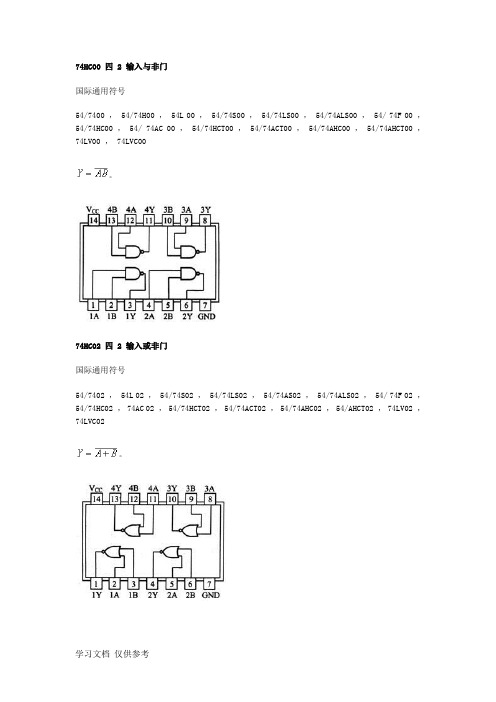
74HC00 四 2 输入与非门国际通用符号54/7400 , 54/74H00 , 54L 00 , 54/74S00 , 54/74LS00 , 54/74ALS00 , 54/ 74F 00 ,54/74HC00 , 54/ 74AC 00 , 54/74HCT00 , 54/74ACT00 , 54/74AHC00 , 54/74AHCT00 ,74LV00 , 74LVC00。
74HC02 四 2 输入或非门国际通用符号54/7402 , 54L 02 , 54/74S02 , 54/74LS02 , 54/74AS02 , 54/74ALS02 , 54/ 74F 02 ,54/74HC02 , 74AC 02 , 54/74HCT02 , 54/74ACT02 , 54/74AHC02 , 54/AHCT02 , 74LV02 ,74LVC02。
74HC04 六反相器国际通用符号54/7404 , 54L 04 , 54/74H04 , 54/74S04 , 54/74LS04 , 54/74AS04 , 54/74ALS04 ,54/ 74F 04 , 54/74HCU04 , 54/74HC04 , 54/ 74AC 04 , 54/74HCT04 , 54/74ACT04 ,54/74AHC04 , 54/74AHCT04 , 74LV04 , 74LVC04 , 54/74AHCU04 , 74LVU04 , 74LVCU04。
74HC08 四 2 输入与门国际通用符号54/7408 , 54/74S08 , 54/74LS08 , 54/74AS08 , 54/74ALS08 , 54/ 74F 08 , 54/74HC08 ,54/74HCT08 , 54/ 74AC 08 , 54/74ACT08 , 54/74AHC08 , 54/74AHCT08 , 74LV08 , 74LVC08。
74HC系列芯片资料

74HC00 四 2 输入与非门国际通用符号54/7400 , 54/74H00 , 54L 00 , 54/74S00 , 54/74LS00 , 54/74ALS00 , 54/ 74F 00 , 54/74HC00 , 54/ 74AC 00 , 54/74HCT00 , 54/74ACT00 , 54/74AHC00 , 54/74AHCT00 ,74LV00 , 74LVC00。
74HC02 四 2 输入或非门国际通用符号54/7402 , 54L 02 , 54/74S02 , 54/74LS02 , 54/74AS02 , 54/74ALS02 , 54/ 74F 02 ,54/74HC02 , 74AC 02 , 54/74HCT02 , 54/74ACT02 , 54/74AHC02 , 54/AHCT02 , 74LV02 , 74LVC02。
74HC04 六反相器国际通用符号54/7404 , 54L 04 , 54/74H04 , 54/74S04 , 54/74LS04 , 54/74AS04 , 54/74ALS04 ,54/ 74F 04 , 54/74HCU04 , 54/74HC04 , 54/ 74AC 04 , 54/74HCT04 , 54/74ACT04 ,54/74AHC04 , 54/74AHCT04 , 74LV04 , 74LVC04 , 54/74AHCU04 , 74LVU04 , 74LVCU04 .74HC08 四 2 输入与门国际通用符号54/7408 , 54/74S08 , 54/74LS08 , 54/74AS08 , 54/74ALS08 , 54/ 74F 08 , 54/74HC08 ,54/74HCT08 , 54/ 74AC 08 , 54/74ACT08 , 54/74AHC08 , 54/74AHCT08 , 74LV08 , 74LVC08。
74LS08中文资料

54/7408四2输入与门简要说明08为四组2输入端与门(正逻辑),共有54/7408、54/74S08、54/74LS08三种线路结构型式,其主要电特性的典型值如下:型号t PLHt phlP D54/7408 17.5ns 12ns 78mW 54/74S08 4.5ns 5ns 125mW 54/74LS08 8ns 10ns 17mW引出端符号1A -4A 输入端 1B -4B 输入端 1Y -4Y 输出端逻辑图双列直插封装极限值电源电压 …………………………………………. 7V 输入电压54/7408、54/74S08………………………………. 5.5V 54/74LS08 ………………………………………. 7V A -B 间电压54/7408、54/74S08..................................... 5.5V 输出截止态电压. (7V)h tt p ://w ww .e l e c f a ns .c om工作环境温度 54XXX ……………………………………………. -55~125℃ 74XXX………… ……………………………… 0~70℃ 存储温度 …………………………………………. -65~150℃功能表:推荐工作条件:5408/7408 54S08/74S08 54LS08/74LS08 最小 额定 最大 最小额定最大 最小额定 最大单位54 4.5 5 5.5 4.5 5 5.5 4.5 5 5.5 电源电压VCC 74 4.75 5 5.25 4.75 5 5.25 4.75 5 5.25V 输入高电平电压V iH2 2 2 V 540.8 0.8 0.7 输入低电平电压V iL74 0.8 0.8 0.8 V 输出高电平电流I OH -800 -1000 -400 µA5416 20 4 输出低电平电流I OL74 16 20 8 mA静态特性(TA 为工作环境温度范围)‘08 ‘S08 ‘LS08 参 数测 试 条 件【1】最小最大最小最大最小 最大单位I ik =-12mA -1.5 V IK 输入嵌位电压 Vcc=最小I ik =-18mA-1.2 -1.5 V54 2.4 2.5 2.5 V OH 输出高电平电压 Vcc =最小V IH =2V ,I OH =最大74 2.4 2.7 2.7 V 54 0.4 0.5 0.4 V OL 输出低电平电压 Vcc=最小,V IL =最大,I OL =最大74 0.4 0.5 0.5 V V I =5.5V 1 1 I I 最大输入电压时输入电流Vcc =最大 V I =7V 0.1 mA V IH =2.4V 40 I IH 输入高电平电流 Vcc =最大V IH =2.7V 50 20µAV IL =0.4V -1.6 -0.4I IL 输入低电平电流 Vcc =最大V IL =0.5V -2mA 54 -20 -55 -40 -100-20 -100I OS 输出短路电流 Vcc =最大74 -18 -55 -40 -100-20 -100mA I CCH 输出高电平时电源电流 Vcc =最大21 32 4.8 mA I CCL 输出低电平时电源电流 Vcc =最大33 57 8.8 mA[1]: 测试条件中的“最小”和“最大”用推荐工作条件中的相应值。
74LS08中文资料
54/7408四2输入与门简要说明08为四组2输入端与门(正逻辑),共有54/7408、54/74S08、54/74LS08三种线路结构型式,其主要电特性的典型值如下:型号t PLHt phlP D54/7408 17.5ns 12ns 78mW 54/74S08 4.5ns 5ns 125mW 54/74LS08 8ns 10ns 17mW引出端符号1A -4A 输入端 1B -4B 输入端 1Y -4Y 输出端逻辑图双列直插封装极限值电源电压 …………………………………………. 7V 输入电压54/7408、54/74S08………………………………. 5.5V 54/74LS08 ………………………………………. 7V A -B 间电压54/7408、54/74S08..................................... 5.5V 输出截止态电压. (7V)h tt p ://w ww .e l e c f a ns .c om工作环境温度 54XXX ……………………………………………. -55~125℃ 74XXX………… ……………………………… 0~70℃ 存储温度 …………………………………………. -65~150℃功能表:推荐工作条件:5408/7408 54S08/74S08 54LS08/74LS08 最小 额定 最大 最小额定最大 最小额定 最大单位54 4.5 5 5.5 4.5 5 5.5 4.5 5 5.5 电源电压VCC 74 4.75 5 5.25 4.75 5 5.25 4.75 5 5.25V 输入高电平电压V iH2 2 2 V 540.8 0.8 0.7 输入低电平电压V iL74 0.8 0.8 0.8 V 输出高电平电流I OH -800 -1000 -400 µA5416 20 4 输出低电平电流I OL74 16 20 8 mA静态特性(TA 为工作环境温度范围)‘08 ‘S08 ‘LS08 参 数测 试 条 件【1】最小最大最小最大最小 最大单位I ik =-12mA -1.5 V IK 输入嵌位电压 Vcc=最小I ik =-18mA-1.2 -1.5 V54 2.4 2.5 2.5 V OH 输出高电平电压 Vcc =最小V IH =2V ,I OH =最大74 2.4 2.7 2.7 V 54 0.4 0.5 0.4 V OL 输出低电平电压 Vcc=最小,V IL =最大,I OL =最大74 0.4 0.5 0.5 V V I =5.5V 1 1 I I 最大输入电压时输入电流Vcc =最大 V I =7V 0.1 mA V IH =2.4V 40 I IH 输入高电平电流 Vcc =最大V IH =2.7V 50 20µAV IL =0.4V -1.6 -0.4I IL 输入低电平电流 Vcc =最大V IL =0.5V -2mA 54 -20 -55 -40 -100-20 -100I OS 输出短路电流 Vcc =最大74 -18 -55 -40 -100-20 -100mA I CCH 输出高电平时电源电流 Vcc =最大21 32 4.8 mA I CCL 输出低电平时电源电流 Vcc =最大33 57 8.8 mA[1]: 测试条件中的“最小”和“最大”用推荐工作条件中的相应值。
74hc08中文资料
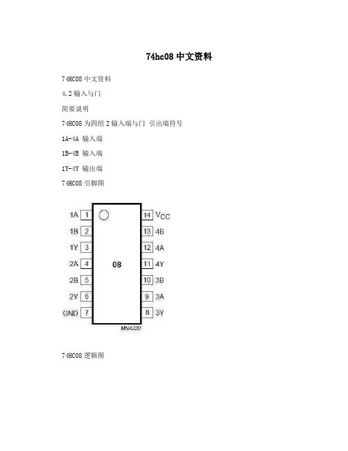
74hc08中文资料74HC08中文资料4,2输入与门简要说明74HC08为四组2输入端与门引出端符号1A-4A 输入端1B-4B 输入端1Y-4Y 输出端74HC08引脚图74HC08逻辑图74HC08功能表极限值电源电压,,,7V输入电压,,,5.5vA,B间电压,,5.5v输出截止电压,,7v工作环境,,,(0,70摄氏度)存储温度,,,(,65,150摄氏度) 文 - 汉语汉字编辑词条文,wen,从玄从爻。
天地万物的信息产生出来的现象、纹路、轨迹,描绘出了阴阳二气在事物中的运行轨迹和原理。
故文即为符。
上古之时,符文一体。
古者伏羲氏之王天下也,始画八卦,造书契,以代结绳(爻)之政,由是文籍生焉。
--《尚书序》依类象形,故谓之文。
其后形声相益,即谓之字。
--《说文》序》仓颉造书,形立谓之文,声具谓之字。
--《古今通论》(1) 象形。
甲骨文此字象纹理纵横交错形。
"文"是汉字的一个部首。
本义:花纹;纹理。
(2) 同本义 [figure;veins]文,英语念为:text、article等,从字面意思上就可以理解为文章、文字,与古今中外的各个文学著作中出现的各种文字字形密不可分。
古有甲骨文、金文、小篆等,今有宋体、楷体等,都在这一方面突出了"文"的重要性。
古今中外,人们对于"文"都有自己不同的认知,从大的方面来讲,它可以用于表示一个民族的文化历史,从小的方面来说它可用于用于表示单独的一个"文"字,可用于表示一段话,也可用于人物的姓氏。
折叠编辑本段基本字义(事物错综所造成的纹理或形象:灿若,锦。
12.刺画花纹:,身。
3(记录语言的符号:,字。
,盲。
以,害辞。
4(用文字记下来以及与之有关的:,凭。
,艺。
,体。
,典。
,苑。
,献(指有历史价值和参考价值的图书资料)。
,采(a(文辞、文艺方面的才华;b(错杂艳丽的色彩)。
5(人类劳动成果的总结:,化。
HD74HC08P中文资料
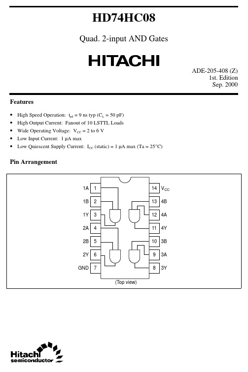
HD74HC08Quad. 2-input AND GatesADE-205-408 (Z)1st. EditionSep. 2000 Features• High Speed Operation: t pd = 9 ns typ (C L = 50 pF)• High Output Current: Fanout of 10 LSTTL Loads• Wide Operating Voltage: V CC = 2 to 6 V• Low Input Current: 1 µA max• Low Quiescent Supply Current: I CC (static) = 1 µA max (Ta = 25°C)Pin ArrangementHD74HC082DC CharacteristicsTa = 25°CTa = –40 to +85°CItem Symbol V CC (V)Min Typ Max MinMax Unit Test ConditionsInput voltageV IH2.0 1.5—— 1.5—V4.5 3.15—— 3.15—6.04.2—— 4.2—V IL2.0——0.5—0.5V 4.5—— 1.35—1.356.0——1.8— 1.8Output voltageV OH2.0 1.9 2.0— 1.9—VVin = V IH or V IL I OH = –20 µA4.5 4.4 4.5— 4.4—6.05.96.0— 5.9—4.5 4.18—— 4.13—I OH = –4 mA 6.05.68——5.63—I OH = –5.2 mAV OL2.0—0.00.1—0.1VVin = V IH or V IL I OL = 20 µA4.5—0.00.1—0.16.0—0.00.1—0.14.5——0.26—0.33I OL = 4 mA 6.0——0.26—0.33I OL = 5.2 mAInput current Iin 6.0——±0.1—±1.0µA Vin = V CC or GNDQuiescent supply currentI CC6.0——1.0—10µAVin = V CC or GND, Iout = 0 µAHD74HC083AC Characteristics (C L = 50 pF, Input t r = t f = 6 ns)Ta = 25°CTa = –40 to +85°CItem SymbolV CC (V)Min Typ Max MinMax Unit Test ConditionsPropagation delay t PHL2.0——90—115nstime4.5—1018—236.0——15—20t PLH 2.0——90—115ns 4.5—818—236.0——15—20Output rise timet TLH2.0——75—95ns 4.5—515—196.0——13—16Output fall timet THL2.0——75—95ns 4.5—515—196.0——13—16Input capacitanceCin——510—10pFHD74HC08 Package Dimensions4HD74HC085HD74HC086Cautions1.Hitachi neither warrants nor grants licenses of any rights of Hitachi’s or any third party’s patent,copyright, trademark, or other intellectual property rights for information contained in this document.Hitachi bears no responsibility for problems that may arise with third party’s rights, includingintellectual property rights, in connection with use of the information contained in this document.2.Products and product specifications may be subject to change without notice. Confirm that you have received the latest product standards or specifications before final design, purchase or use.3.Hitachi makes every attempt to ensure that its products are of high quality and reliability. However,contact Hitachi’s sales office before using the product in an application that demands especially high quality and reliability or where its failure or malfunction may directly threaten human life or cause risk of bodily injury, such as aerospace, aeronautics, nuclear power, combustion control, transportation,traffic, safety equipment or medical equipment for life support.4.Design your application so that the product is used within the ranges guaranteed by Hitachi particularly for maximum rating, operating supply voltage range, heat radiation characteristics, installationconditions and other characteristics. Hitachi bears no responsibility for failure or damage when used beyond the guaranteed ranges. Even within the guaranteed ranges, consider normally foreseeable failure rates or failure modes in semiconductor devices and employ systemic measures such as fail-safes, so that the equipment incorporating Hitachi product does not cause bodily injury, fire or other consequential damage due to operation of the Hitachi product.5.This product is not designed to be radiation resistant.6.No one is permitted to reproduce or duplicate, in any form, the whole or part of this document without written approval from Hitachi.7.Contact Hitachi’s sales office for any questions regarding this document or Hitachi semiconductor products.Hitachi, Ltd.Semiconductor & Integrated Circuits.Nippon Bldg., 2-6-2, Ohte-machi, Chiyoda-ku, Tokyo 100-0004, Japan Tel: Tokyo (03) 3270-2111 Fax: (03) 3270-5109Copyright © Hitachi, Ltd., 2000. All rights reserved. Printed in Japan.Hitachi Asia Ltd. Hitachi Tower16 Collyer Quay #20-00, Singapore 049318Tel : <65>-538-6533/538-8577 Fax : <65>-538-6933/538-3877URL : .sg URLNorthAmerica : /Europe : /hel/ecg Asia : Japan : http://www.hitachi.co.jp/Sicd/indx.htmHitachi Asia Ltd.(Taipei Branch Office)4/F, No. 167, Tun Hwa North Road, Hung-Kuo Building, Taipei (105), Taiwan Tel : <886>-(2)-2718-3666 Fax : <886>-(2)-2718-8180 Telex : 23222 HAS-TPURL : Hitachi Asia (Hong Kong) Ltd. Group III (Electronic Components) 7/F., North Tower, World Finance Centre,Harbour City, Canton Road Tsim Sha Tsui, Kowloon, Hong KongTel : <852>-(2)-735-9218 Fax : <852>-(2)-730-0281URL : Hitachi Europe Ltd.Electronic Components Group.Whitebrook ParkLower Cookham Road MaidenheadBerkshire SL6 8YA, United Kingdom Tel: <44> (1628) 585000Fax: <44> (1628) 585160Hitachi Europe GmbHElectronic Components Group Dornacher Stra βe 3D-85622 Feldkirchen, Munich GermanyTel: <49> (89) 9 9180-0Fax: <49> (89) 9 29 30 00Hitachi Semiconductor (America) Inc.179 East Tasman Drive,San Jose,CA 95134 Tel: <1> (408) 433-1990Fax: <1>(408) 433-0223For further information write to:Colophon 2.0。