Improved microwave circuit design using multipoint-response-correction space mapping and trust
关于仿真软件ads的书

关于仿真软件ads的书关于仿真软件ADS(Advanced Design System)的书籍,以下是一些可能的参考:1. "Advanced Design System (ADS) Tutorial Guide" by Keysight Technologies: 这是一本官方教程指南,详细介绍了ADS的各种功能和使用方法。
2. "Microwave Office and ADS Circuit Design and Simulation" by Joseph F. White: 这本书涵盖了ADS和其他微波电路设计与仿真软件的使用,包括滤波器、放大器、混频器等电路的设计和优化。
3. "RF and Microwave Circuit Design for Wireless Systems" by David Pozar: 虽然这本书不是专门针对ADS的,但它包含了大量关于射频和微波电路设计的内容,这些内容在使用ADS进行仿真时非常有用。
4. "IC Design for Reliability" by J. R. Davis: 这本书讨论了集成电路设计中的可靠性问题,并包含了一些使用ADS进行仿真和分析的例子。
5. "High-Frequency Techniques: An Introduction to RF and Microwave Engineering" by Frederic J. Gardiol: 这本书是射频和微波工程的入门教材,其中包括了一些使用ADS进行仿真和设计的实例。
以上书籍都可以在各大线上书店或者图书馆找到。
不过需要注意的是,由于ADS软件的更新换代,一些旧版书籍中的内容可能与最新版本的ADS 有所差异,因此在使用时需要结合软件的实际版本进行参考。
一种2_45GHz微波二极管整流电路
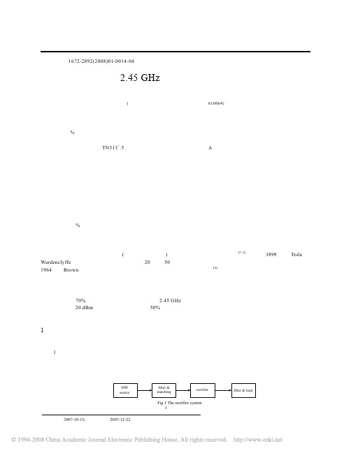
第6卷 第1期信息与电子工程Vo1.6,No.1 2008年2月INFORMATION AND ELECTRONIC ENGINEERING Feb.,2008文章编号:1672-2892(2008)01-0014-04一种2.45 GHz微波二极管整流电路罗 俊,何其娟,刘长军(四川大学 电子信息学院,四川 成都 610064)摘要:为了提高用于微波无线功率传输的微波整流效率,本文采用微带结构实现了一个2.45GHz的微波二极管整流电路。
仿真实验结果证明在输入功率约为20 dBm的情况下,获得了大于50%的整流效率。
通过完善和改进电路,可以进一步提高整流的效率,并应用于微波整流天线。
关键词:微波整流;整流天线;微波输能中图分类号:TN313+.5 文献标识码:AExperiments on a 2.45 GHz Microwave Diode RectifierLUO Jun,HE Qi-juan,LIU Chang-jun(School of Electronics and Information Engineering, Sichuan University,Chengdu Sichuan 610064,China)Abstract:Recently the research on microwave wireless power transmission has attracted more and more interests. As an essential part of a microwave wireless power transmission system, the microwaverectifier has been well studied. In this paper, a 2.45 GHz microwave diode rectifier based on microstriptransmission line structures is implemented. The measured microwave rectification efficiency is higherthan 50%when the input microwave power is about 20 dBm. In future, the microwave rectificationefficiency can be further improved with better circuit designs.Key words:microwave rectification;rectenna;microwave power transmission近年来,微波无线功率传输(也称为微波输能)引起了人们越来越多的关注[1-3]。
rf and microwave circuit design pdf

rf and microwave circuit design pdfRF (Radio Frequency) and Microwave Circuit Design is a crucial area in the realm of electronics engineering. This technology enables the development of wireless communication systems, such as radio broadcasting, satellite communication, mobile networks, and radar systems. An RF and MicrowaveCircuit Design PDF provides a comprehensive guide to the theory, design, and implementation of RF and microwave circuits. In this article, we will discuss the various steps involved in RF and Microwave Circuit Design.Step 1: Understanding the Basics of RF and Microwave Circuit DesignBefore starting the design process, it is essential to have a solid grasp of the theory and concepts behind RF and Microwave circuitry. This includes understanding electromagnetic waves, transmission lines, impedance matching, and various other aspects of the RF and microwave spectrum.Step 2: Selecting the Desired Frequency BandThe selection of a frequency band is a critical step in the design process. The band of frequencies that you choose will depend on the particular application of the circuit. For example, a circuit designed for wireless communication will typically operate in the GHz (Gigahertz) range, while acircuit for a radar system might operate in the low MHz (Megahertz) range.Step 3: Designing the Circuit SchematicThe circuit schematic is the blueprint for the actualhardware implementation of the RF or microwave circuit. It isessential to design a schematic that accurately represents the desired functionality of the circuit. This includes selecting appropriate active and passive components, such as transistors, diodes, capacitors, and resistors.Step 4: Simulating and Testing the Circuit Design Simulating and testing the circuit design is a crucial stepin the design process. Computer-aided design (CAD) software can be used to simulate the circuit, enabling the designer to identify potential problems and modify the design as needed. Once the simulation is complete, the circuit should be tested in a real-world environment to ensure that it meets the desired specifications and performance requirements.Step 5: Fabricating the PCB BoardOnce the circuit design has been simulated and tested successfully, it is time to fabricate the printed circuit board (PCB). The PCB is the physical implementation of the circuit schematic and is the backbone of the overall circuit design.Step 6: Final Assembly and TestingThe final step in the design process is to assemble and test the completed circuit. This includes soldering components to the PCB, connecting any external components or peripherals, and conducting comprehensive testing to ensure that thecircuit meets the desired specifications and performance requirements.In conclusion, RF and microwave circuit design is a complex and critical area in electronics engineering. The design process involves understanding the theory and concepts of RF and Microwave circuitry, selecting the desired frequency band, designing the circuit schematic, simulating and testing the circuit design, fabricating the PCB board,and final assembly and testing. By following these steps, electronics engineers can design and implement high-performance RF and Microwave circuits that are optimized for their specific applications.。
超宽带微带带通滤波器的设计

超宽带微带带通滤波器的设计袁伟强;宋树祥;程洋;张勇敢【摘要】为了设计小型化、低插入损耗、宽阻带的滤波器,本文基于缺陷微带结构(defected microstrip structure,DMS)提出一种新型H形DMS结构微带滤波器,利用DMS结构与1/4波长终端短路谐振器设计制作一种小型超宽带微带带通滤波器,并用ADS(advanced design system)软件对该滤波器进行分析及仿真验证,且对所设计的滤波器进行实物加工测试.测试结果表明,该滤波器的相对带宽达到了116%,阻带在-20 dB以下的频段为12~19 GHz,其宽度达到了7 GHz,与理论分析基本一致.该滤波器尺寸为13.7 mm×6.8 mm,同时还具有插入损耗小、结构简单紧凑等优点.%Based on the defected microstrip structure (DMS),a new H-shaped DMS microstrip filter is proposed.A small ultra-wideband microstrip bandpass filter is designed and fabricated using the DMS structure and the 1/4 wavelength shorted resonator.The filter is analyzed and simulated by ADS software.The designed filter is tested by physical processing.The test results show that the relative bandwidth of the filter reaches 116%,and the band with -20 dB is 12-19 GHz and its width is 7 GHz, which is consistent with the theoretical analysis.The size of the filter is 13.7 mm× 6.8 mm,with a small insertion loss,simple structure,and other advantages.【期刊名称】《广西师范大学学报(自然科学版)》【年(卷),期】2017(035)004【总页数】7页(P32-38)【关键词】带通滤波器;缺陷微带结构(DMS);超宽带;短路枝节;ADS【作者】袁伟强;宋树祥;程洋;张勇敢【作者单位】广西师范大学电子工程学院,广西桂林 541004;广西师范大学电子工程学院,广西桂林 541004;广西师范大学电子工程学院,广西桂林 541004;广西师范大学电子工程学院,广西桂林 541004【正文语种】中文【中图分类】TN713近些年,超宽带技术蓬勃发展,自2002年美国通信委员会(federal communications commission,FCC)批准超宽带可以商业使用以来,各种超宽带器件的研究逐渐增加。
英语作文-集成电路设计的未来发展趋势与技术创新

英语作文-集成电路设计的未来发展趋势与技术创新The Future Development Trends and Technological Innovations of Integrated Circuit Design。
In recent years, integrated circuit (IC) design has been advancing at an unprecedented pace, revolutionizing various industries and transforming the way we live. As we look ahead, it is crucial to understand the future development trends and technological innovations that will shape the field of IC design. This article aims to explore these trends and innovations, shedding light on the exciting possibilities that lie ahead.One of the key trends in IC design is the move towards smaller and more powerful chips. Over the years, the size of ICs has been shrinking, allowing for more transistors to be packed onto a single chip. This trend, known as Moore's Law, has been driving the rapid advancement of technology. However, as the size of transistors approaches its physical limits, alternative approaches such as three-dimensional (3D) integration and nanotechnology are being explored.3D integration involves stacking multiple layers of transistors on top of each other, enabling higher transistor density and improved performance. This approach not only allows for greater miniaturization but also reduces power consumption and improves signal integrity. Furthermore, nanotechnology, which involves manipulating individual atoms and molecules, holds immense potential for IC design. By harnessing the unique properties of nanomaterials, such as carbon nanotubes and graphene, researchers can create faster, more energy-efficient transistors.Another important trend in IC design is the increasing focus on energy efficiency. With the growing demand for portable devices and the need to reduce energy consumption, power-efficient ICs have become a top priority. This has led to thedevelopment of low-power design techniques, such as voltage scaling, clock gating, and power gating. These techniques aim to minimize power consumption during both active and idle states, extending battery life and reducing environmental impact.Furthermore, the emergence of artificial intelligence (AI) and machine learning (ML) has had a profound impact on IC design. AI and ML algorithms are being used to optimize various aspects of the design process, including floor planning, placement, routing, and timing closure. By leveraging the power of AI, designers can achieve higher performance, lower power consumption, and shorter time-to-market. Moreover, AI is also being utilized for fault detection and diagnosis, improving the reliability and yield of ICs.In addition to these trends, technological innovations such as photonic integration and quantum computing are poised to reshape the future of IC design. Photonic integration involves the integration of optical components, such as lasers and waveguides, on a single chip. This enables high-speed data transmission and offers significant advantages over traditional electronic interconnects in terms of bandwidth and latency. On the other hand, quantum computing leverages the principles of quantum mechanics to perform complex computations at an unprecedented scale. While still in its infancy, quantum computing has the potential to revolutionize fields such as cryptography, optimization, and drug discovery.In conclusion, the future of IC design holds immense promise, with numerous trends and technological innovations shaping its trajectory. From smaller and more powerful chips to energy-efficient designs and the integration of AI and ML, the field is poised for remarkable advancements. Additionally, the emergence of photonic integration and quantum computing opens up new frontiers for exploration. As researchers and engineers continue to push the boundaries of what is possible, the future of IC design is set to be a thrilling journey of innovation and discovery.。
射频工程师必读书籍

ADS,MWO,Ansoft还是CST、HFSS频微波类书希望对大家有点帮助:1.《射频电路设计--理论与应用》『美』Reinhold Ludwig 著电子工业出版社个人书评:射频经典著作,建议做RF的人手一本,里面内容比较全面,这本书要反复的看,每读一次都会更深一层理解.随便提一下,关于看射频书籍看不懂的地方怎么办?我提议先看枝干或结论有个大概印象,实在弄不明白就跳过(当然可问身边同事同学或GOOGLE一下),跳过不是不管它了,而是尽量先看完自己能看懂的,看第二遍的时候再重点抓第一次没有看懂的地方,人的思维是不断升华的,知识的也是一个系统体系,有关联的,当你把每一块砖弄明白了,就自然而然推测出金字塔塔顶是怎么架设出来的。
2. 《射频通信电路设计》『中』刘长军著科学技术出版社个人书评:有拼凑之嫌(大量引用书1和《微波晶体管放大电路分析与设计》内容),但还是有可取之处,加上作者的理解,比看外文书(或者翻译本)看起来要通俗易懂,毕竟是中国人口韵。
值得一看,书上有很多归纳性的经验.3.《高频电路设计与制作》『日』市川欲一著科学技术出版社个人书评:本人说实话比较喜欢日本人写书的风格和语言,及其通俗,配上图示,极其深奥的理论看起来明明朗朗,比那些从头到尾只会搬抄公式的某些教授强们多了,本书作者的实践之作,里面都是一些作者的设计作品和设计方法,推荐一看.4. 《LC滤波器设计与制作》『日』森荣二著科学技术出版社个人书评:语言及其通俗易懂,完全没有深奥的理论在里面,入门者看看不错,但是设计方法感觉有点落后,完全手工计算.也感觉内容的太细致,此书一般.5. 《振荡电路设计与应用》『日』稻叶宝著科学技术出版社个人书评:这边书还不错,除了学到振荡电路设计,还学到了很多模拟电路的基础应用,唯一缺点书中的内容涉及频率的都不够高(k级,几M,几十,几百M的振荡器),做有源电路的可以看一下,整体感觉还行.6. 《锁相环电路设计与应用》『日』远坂俊昭著科学技术出版社个人书评:对PLL原理总是搞不太明白的同学可以参考此书,图形图片很多,让人很直观明白,比起其他PLL书只会千篇一律写公式强千倍。
射频微波通讯电路设计(RF-Microwave Communication Circuits Design )
ε eff = λ
(e) (o) ε eff + ε eff
2
c
=
λ0 f l= = = 4 4 ε eff 4 ε eff
求 Z0e,Z0o: c = 10−20 / 20 = 0.1 Z 0e = Z 0 Z 0e = Z 0
3.7365 + 3.2195 = 1.8636 2 3 × 10¹¹ 5.8 × 109 = 6.9387mm = 4 × 1.8636
其中 L,C,CC 計算如下
L= C= Z0 50 = = 1.372 × 10⁻⁹ H 9 2π f 0 2π × 5.8 × 10 1 1 = = 5.488 × 10⁻¹³ F 9 2π f 0 Z 0 2π × 5.8 × 10 × 50 10 10 = = 5.488 × 10⁻¹⁴ F 9 2π f 0 Z 0 2π × 5.8 × 10 × 50
CF 20 −20 20
CC : Coupling Capacitance CC < 0.18 / 2πf0 CF: Coupling Factor
CC =
S-parameter analyze: The magnitude of S11,S21,S31,S41(dB)
Return Loss = -20Log(S11) =39.99 dB Coupling = -10Log(P3/P1) = 19.96 dB Isolation = -10Log(P4/P1) = 40.00 dB Directivity = -10Log(P4/P3) = Isolation – Coupling = 40 – 19.96 = 20.04 dB Insertion Loss = -10Log(1-P3/P1) = 0.0436 dB
IMPROVE (24)
Journal of the European Ceramic Society27(2007)2941–2944Multilayer thick-film technology as applied todesign of microwave devicesPolina V.Kapitanova a,∗,Alexander V.Simine b,1,Dmitry V.Kholodnyak a,Irina B.Vendik aa St.Petersburg Electrotechnical University,Department of Microelectronics&Radio Engineering,5,Prof.Popov st.,197376,St.Petersburg,Russiab Innovation Center RF NXP Semiconductors,Gerstweg2,6534AE Nijmegen,The NetherlandsAvailable online8January2007AbstractPossibilities of the sandwich multilayer technology to design microwave integrated circuits are discussed.Original designs of various passive microwave devices realized as multilayer sandwich structures are presented.Experimental results confirmed a good potential of the sandwich technology to design high-performance multilayer microwave integrated circuits.©2006Elsevier Ltd.All rights reserved.Keywords:Microwave integrated circuits(MICs)1.IntroductionThe low temperature co-fired ceramics(LTCC)technology is generally used to fabricate multilayer microwave integrated circuits(MICs).1–4Allocation of passive components within several layers makes it possible to design highly integrated MICs of a small size.The low-cost LTCC technology using the screen-printing technique suits well for a mass production of microwave devices with improved price/performance.The thick-film sandwich technology was shown to be an alter-native to the LTCC one regarding a design of microwave devices as multilayer MICs.5Microwave devices using transmission line sections are of a large size at low microwave frequencies and exhibit a spurious response.At the same time,the both multilayer technologies allow designing very compact and free of spurious response microwave devices based on quasi-lumped components.The goal of this paper is to demonstrate a good poten-tial of the sandwich technology for the design of multilayer MICs.Miniature quasi-lumped-element bandpassfilter,3and 10-dB directional couplers,and a balun for wireless applications were designed as multilayer sandwich structures,fabricated and experimentally investigated.∗Corresponding author.Tel.:+78123460867;fax:+78123460867.E-mail addresses:MWLab@eltech.ru(P.V.Kapitanova),Alexander.simin@(A.V.Simine).1Tel:+31243535303;fax:+31243536556.2.The sandwich multilayer technologyThough the sandwich multilayer technology is quite sim-ilar to the LTCC one,there are some principal differences between them.The LTCC technology uses the screen-printing technique for metallization patterning over thin dielectric sheets (∼100m).Patterned sheets are stacked up,laminated andfired under the temperature of about850◦C.One can say that met-allization patterning in the LTCC technology is fabricated“in parallel”.In turn,a thick ceramic substrate is used as the core of multilayer structure in the sandwich technology.Conductive and dielectric pastes are,respectively,applied for metallization patterning and fabrication of additional thin dielectric layers on the both sides of the thick ceramic substrate.A typical layer thickness is15m for the conductive layers and60m for the dielectric ones.The layers are deposited“in series”manner with a consecutive co-firing of each layer.The co-firing temperature is approximately the same as for the LTCC structures—up to 900◦C.The sandwich multilayer technology have the following advantages for MICs realization with respect to the LTCC process:(i)smaller thickness of dielectric layers with respect to LTCC materials allows decreasing the area occupied by parallel-plate capacitors;(ii)parasitic grounded capacitances are sufficiently eliminated due to using of the thick sub-strate.The sandwich process is compatible with planar thin-film technology.The ceramic substrate employed in the sandwich0955-2219/$–see front matter©2006Elsevier Ltd.All rights reserved. doi:10.1016/j.jeurceramsoc.2006.11.0192942P.V.Kapitanova et al./Journal of the European Ceramic Society27(2007)2941–2944Fig.1.Equivalent circuit(a),multilayer implementation(b)and characteristics (c)of the three-pole bandpassfilter.structures could play the role of PCB,onto which a front-end module would assembled.3.Passive microwave devices realized as sandwich multilayer structuresThe three-pole Chebyshev bandpassfilter for Bluetooth and WLAN applications(2400–2500MHz)was designed as a sand-wich multilayer structure based on quasi-lumped-elements.The equivalent circuit of thefilter is shown in Fig.1a.Thefilter struc-ture(Fig.1b)uses two60-m thick dielectric layers with the dielectric constantεr=10.2and the loss tangent tanδ=0.002, which are situated underneath the1-mm thick alumina substrate. Grounded capacitances were realized as parallel-plate capaci-tors.Serial coupling capacitances were produced by overlaying electrodes of the capacitors situated in different layers.Inductors were designed as transmission line sections of corresponding length.The microstrip feed lines placed on the top surface of the substrate are connected to thefilter by via holes.The sil-ver paste with R dc=0.02 /square was used for15-m thick metallization pattern.The size of the sandwichfilter structureis Fig.2.Equivalent circuit(a),layout(b)and photograph(c)of a directional coupler accomplished by the sandwich multilayer technology.P .V .Kapitanova et al./Journal of the European Ceramic Society 27(2007)2941–294429438.7mm ×4.5mm.Characteristics obtained by the electromag-netic simulation of the lossless and lossy filter structures are presented in Fig.1c.The in-band insertion loss does not exceed 4dB and the return loss is better than 20dB.Two quasi-lumped-element directional couplers with the cou-pling value of 3and 10dB were implemented using the sandwich multilayer technology.The equivalent circuit shown in Fig.2a was obtained by replacing the quarter-wavelength transmission line sections of a conventional branch-line directional cou-pler by lumped-element -networks.The 50 transmission line sections were replaced by the -networks consisting of serial inductance and parallel capacitances,whereas the 35 transmission line sections were replaced by the capacitive -networks representing an impedance inverter.Fig.2b shows the layout of the directional coupler containing parallel-plate capac-itors and two-turn stacked inductors,which are situated within two conductive layers on 1-mm thick alumina substrate.The size of the 3and 10-dB directional couplers is 5.9mm ×5.2mm and 7.2mm ×6.5mm,correspondingly.The photograph of the 3-dB directional coupler is shown in Fig.2c.Measured characteristics of the devices are presented in Fig.3.In general,the experimen-tal data are in a good agreement with the simulation results.For the both directional couplers in the operating frequency band (2400–2500MHz),the measured return loss and the isolation are better than 20dB.Measured insertion loss is about 0.5dB.The amplitude unbalance is better than ±0.5dB,and the phase error is less than ±1.5◦.The rat-race ring is often used as a matched balun.However,a large size limits its application at low microwave frequen-cies.Replacing the 270◦transmission line section in therat-raceFig.3.Measured characteristics of the directional couplers with the 3-dB (a)and 10-dB (b)coupling.Fig.4.Equivalent circuit (a),layout of multilayer MIC (b)and photograph (c)of the balun.ring by a lumped-element impedance inverter as a capacitive -network may solve the problem.Other three 90◦transmission line sections of the rat-race ring can be replaced by lumped-element -networks consisting of serial inductance and parallel capacitances.The equivalent circuit is illustrated by Fig.4a.The sandwich implementation of the balun is shown in Fig.4b.The device uses 1-mm thick alumina substrate with one addi-tional dielectric layer and three conductive ing the thick ceramic substrate allows eliminating an influence of par-asitic capacitance to the ground.The size of the matched balun designed for the frequency 2.45GHz is 13mm ×12mm.The photograph of the matched balun is shown in Fig.4c.Results of electromagnetic simulation of the lossy balun structure are presented in Fig.5,in a comparison with measured character-istics.According to the simulation results,the device provides in the frequency range 2.2–2.7GHz the equal power splitting with the amplitude unbalance ±1dB.The return loss is bet-ter than 25dB and the isolation is not worse than 20dB.The insertion loss is about 0.2dB.The phase difference is 180±5◦.The measured data are in a good coincidence with the simulated2944P.V.Kapitanova et al./Journal of the European Ceramic Society27(2007)2941–2944Fig.5.Characteristics of the balun(simulated results,dashed lines;measured data,solid lines).ones,excepting a slight shift of the characteristics to the lower frequency.4.ConclusionThe original design of the miniature quasi-lumped-element bandpassfilter,two directional couplers and the matched balun realized as multilayer MICs using the sandwich technology were presented.A good coincidence between the simulated and mea-sured characteristics was observed for all the devices under investigation.The insertion loss of the microwave devices manu-factured by the sandwich technology could be reduced by using conductive pastes with as lower surface impedance as in the LTCC technology.References1.Lucero,R.,Qutteneh,W.,Pavio,A.,Meyers,D.and Estes,J.,Design of anLTCC switch diplexer front-end module for GSM/DCS/PCS applications.In Proceedings of IEEE Radio Frequency Integrated Circuits Symposium,2001, pp.213–216.2.Pinel,S.,Chakraborty,S.,Roellig,M.,Kunze,R.,Mandal,S.,Liang,H.et al.,3D integrated LTCC module using BGA technology for compact C-band RF front-end module.In Proceedings of IEEE MTT-S Int.Microwave Symposium Digest,2002,pp.1553–1556.3.Heide,P.,Chernyakov,A.,Markov,K.,Kryshtopin,A.,Orlenko,D.,Royak,S.et al.,Highly-integrated LTCC front-end-modules for Bluetooth and wireless-LAN applications.In Proceedings of6th European Conference on Wireless Technology,2003,pp.359–362.4.Chernyakov, A.,Markov,K.,Kryshtopin, A.,Orlenko, D.,Royak,S.,Kravchenko,R.et al.,Novel small-size LTCC-based WLAN frontend-modules with integrated power amplifiers.In IEEE MTT-S Int.Microwave Symposium Digest,2004,pp.559–562.5.Kapitanova,P.,Simine,A.,Kholodnyak,D.and Vendik,I.,Application ofsandwich multilayer technology to MICs design.In Proceedings of35th European Microwave Conference,2005,pp.389–392.。
- 1、下载文档前请自行甄别文档内容的完整性,平台不提供额外的编辑、内容补充、找答案等附加服务。
- 2、"仅部分预览"的文档,不可在线预览部分如存在完整性等问题,可反馈申请退款(可完整预览的文档不适用该条件!)。
- 3、如文档侵犯您的权益,请联系客服反馈,我们会尽快为您处理(人工客服工作时间:9:00-18:30)。
Improved Microwave Circuit Design using Multipoint-Response-Correction Space Mapping and Trust RegionsSlawomir Koziel, Senior Member, IEEEEngineering Optimization & Modeling Center, School of Science and Engineering, Reykjavik University, Kringlunni 1, IS-103 Reykjavik, IcelandAbstract—Space mapping (SM) technology includes so-called output SM that ensures exact matching between the surrogate and the fine model at the current design. Output SM exploits the fine model data at a single design and is not able to align the models’ sensitivity. Here, a multipoint response correction is introduced that generalizes the concept of output SM. By using a design-variable-dependent correction term and exploiting all available fine model information, the proposed technique provides exact match between the surrogate and the fine model at several designs. This not only retains the benefits of output SM but also enhances sensitivity matching between the two models, which results in improved performance of the SM optimization process. Verification using two microwave design problems is provided.Index Terms—Computer-aided design(CAD), EM optimization, surrogate modeling, response correction, space mapping.I. I NTRODUCTIONEfficient EM-simulation-based optimization of CPU-intensive structures can be realized using surrogate models [1]. One of the most successful approaches of this kind in microwave engineering is space mapping (SM) [2]-[6]. SM replaces the optimization of expensive or “fine” model by means of the iterative optimization and updating of so-called “coarse” model which is less accurate but cheaper to evaluate. Early versions of space mapping, here referred to as input-like-SM, were focused on transformation of the coarse model domain using shifts and/or variable scaling [2]. Flexibility of the coarse model can be enhanced by implicit SM [4] that exploits so-called preassigned parameters: non-optimizable variables that are fixed in the fine model (e.g., dielectric constants) but adjustable in the coarse model. In many cases, however, neither input nor implicit SM is able to provide sufficient alignment between the coarse and the fine model. Performance of SM algorithms can be improved using output SM [2], in which the coarse model is enhanced using a correction term that allows us to obtain a perfect matching between the coarse and the fine model at the current iteration point [3]. This correction term is a constant vector calculated using fine model data at a single (most recent) design [3]. Output SM usually improves the performance of the SM algorithm, particularly when used with the trust region (TR) This work was supported in part by the Reykjavik University Development Fund under Grant T09009.S. Koziel is with the Engineering Optimization & Modeling Center, School of Science and Engineering, Reykjavik University, Menntavegur 1, IS-101 Reykjavik, Iceland. approach [7], [8]. However, output SM ensures, at most, zero-order consistency between the coarse and the fine model [8], which may result in premature termination of the optimization process at the design that is far from the optimum [8]. This problem arises, in particular, when the model responses are very nonlinear, a common situation in microwave engineering.In this paper, a multi-point response correction is introduced that generalizes the concept of output SM. A design-variable-dependent correction term is constructed that ensures perfect matching between the coarse and the fine model at a number of previously considered designs. The proposed approach ensures approximate satisfaction of the first-order consistency condition [9] and improves the performance of the SM optimization process when compared to the output SM. Two microwave design problems are presented for verification purposes.II. R ESPONSE C ORRECTION:O UTPUT S PACE M APPINGLet R f : X f →R m,X f⊆R n, denote the response vector of a fine model of the device of interest, e.g., S-parameters evaluated at m different frequencies. Our goal is to solve*arg min(())ff fXU∈=xx R x(1) where U is a scalar objective function, e.g., minimax [2]. Space mapping avoids solving (1) directly. Instead, it produces a sequence of approximate solutions to (1), x(i), i = 0, 1, 2, …, as:()(1)()arg min()i isU+=xx R x(2) where R s(i) is the surrogate model at iteration i.Let R c : X c→R m,X c⊆R n,denote the response vectors of the coarse model: computationally cheap but relaxed-accuracy representation of the fine model. The surrogate model R s(i) is constructed from the coarse model as follows()()().()()i i is c sm=+R x R x d(3) Here, R c.sm(i) denotes R c composed with suitable SM transformations. For example, in case of input SM we have R c.sm(i)(x) = R c(B(i)·x + c(i)), where the n×n matrix B(i) and n×1 vector c(i) are obtained using parameter extraction [2].The output SM correction term d(i) is defined as [3]()()()().()()i i i if c sm=−d R x R x(4) This definition ensures zero-order consistency between the fine model and the SM surrogate at x(i), i.e., R f(x(i)) = R s(i)(x(i)).III. M ULTIPOINT R ESPONSE C ORRECTION T ECHNIQUE The output SM correction term d (i )is defined using the R f response at the current iteration point x (i ). Here, a multipoint response correction is proposed that exploits most of the available R f data. In particular, we want to define the model()()()().()()()i i i i s c sm g =+R x R x ΔR x (5)so that the correction term ΔR g (i ) has the following features: (i) ΔR g (i )(x (i )) = R f (x (i )) – R c.sm (i )(x (i )), i.e., R s (i )(x (i )) = R f (x (i )), (ii) R s (i )(x (k )) = R f (x (k )), i.e., ΔR g (i )(x (k )) = R f (x (k )) – R c.sm (i )(x (k )) for as many k < i as possible,(iii) ΔR g (i ) is a linear function of x (so that it does not degrade the ability of R c to model higher order nonlinearities of R f ), Let S (i ) be a set of all affinely independent subsets of X (i ) = {x (1), x (2), …, x (i )} containing x (i ). Let s (i )∈S (i ) be such that: (i) s (i ) is maximal, i.e., |s (i )| = n i = max{|s | : s ∈ S (i )}, and (ii) s (i ) is the smallest in the sense of its diameter, i.e., d (s (i )) = min{d (s ) : s ∈ S (i ) ∧ |s | = n i }, where d (s ) ≡ max{||x – y || : x , y ∈ s }. We have |s (i )| ≤ min(i , n + 1). Let x k , k = 1, 2, …, n i , denote the elements of s (i ) (here, x 1 = x (i )). Define R k = R f (x k ) – R c.sm (i )(x k ), k = 1, 2, …, n i . Let us also define the m ×n i matrix R (i ) = [R 1 R 2 … R n i ].Let M (i ) ⊆ R n be a linear manifold generated by s (i ), i.e.,{}()11:,1i i n ni n k k k k k M R αα===∈==∑∑x x x (6)M (i ) is well defined because s (i ) is affinely independent. Let B (i ) = {b 1, …, b n i –1}, where b k = x k +1 – x 1, k = 1, 2, …, n i – 1. Now, let Y (i ) ⊆ R n be a linear subspace generated by B (i ), i.e.,{}1()1:,,1,2,...,1i n i n k k k i k Y R R k n ββ−==∈=∈=−∑x x b (7)Clearly, Y (i ) = M (i ) – x (i ). For any x ∈ R ndefine P i (x ) as the orthogonal projection of x – x (i ) onto Y (i ). For any y ∈ M (i ) define λi (y ) = [λ1 λ2 … λn i ]T so that y = λ1x 1 + λ2x 2 + … + λn i x n i . λi is uniquely determined and λ1 + λ2 + … + λn i = 1. We can now define ΔR g (i )(x ), x ∈ R n , as()()()().()()()()()for 1()(())for 1i i i i f c sm gi i i i i i P i ⎧−==⎨⋅−+>⎩R x R x ΔR x R λx x x(8)In (8), we distinguished two cases (i = 1 and i > 1) becausesome of the above objects (e.g., Y (i )) are not defined for i = 1. Fig. 1 illustrates the concepts used to define ΔR g (i )( ⋅ ).Vector λi (y ) can be determined by solving a linear system()()i i i =T λy (9)where T (i )is (n +1) × n i matrix defined as()()1(1)0[11...1]1i i i n ×−⎡⎤=⎢⎥⎢⎥⎣⎦B T(10)with B (i ) being the n ×(n i -1) matrix such that its k th column is avector b k , and y (i ) is (n +1)×1 vector()()()()1i i i i P ⎡⎤−+=⎢⎥⎣⎦x x x y(11)Because vectors b k , k = 1, 2,…, n i – 1, are linearly independent,solution to (9) can be found as()1()()()()i T i i T i i −=λT T T y (12)Fig. 1. Illustration of the objects used to define the multipoint response correction model ΔR g (x (i )) for n = 3.It follows, that ΔR g (i ) satisfies properties (i)-(iii) listed at the beginning of this section. In particular, if x = x (i ), then P i (x – x (i )) = 0 and λi (P i (x – x (i )) + x (i )) = λi (x (i )) = [1 0 … 0]T ; consequently, ΔR g (i )(x (i )) = R (i )⋅[1 0 … 0]T = R 1 = R f (x (i )) – R c.sm (i )(x (i )). In general, ΔR g (i )(x k ) = R k = R f (x k ) – R c.sm (i )(x k ) for all k = 1, 2,…, n i ; hence, as s (i ) is maximal, we have ΔR g (i )(x k ) = R f (x k ) – R c.sm (i )(x k ) for as many k as possible taking into account other constraints for our mapping. Finally, ΔR g (i ) is linear, because P i , λi , and multiplication R (i )⋅λi are linear. It should be noted, that ΔR g (i ) contains some information about the Jacobian of R f (x (i )) – R c.sm (i )(x (i )). In particular, the Jacobian of ΔR g (i ) is the approximation of the Jacobian reduced to the subspace Y (i ). Note also that ΔR g (i ) is constant along all directions orthogonal to Y (i ). Moreover, it can be shown, that if d (s (i )) → 0, then ()()().()()()()|i i i gf c smi i Y J J −→ΔR R R x x ,i.e., given the diameter of s (i ) going to zero, the Jacobian ofΔR g (i ) becomes more and more accurate approximation of Jacobian of R f (x (i )) – R c.sm (i )(x (i )), reduced to Y (i ). In particular, if |s (i )| = n + 1, then the Jacobian of ΔR g (i ) becomes good approximation of Jacobian of R f (x (i )) – R c.sm (i )(x (i )) on R n , provided that d (s (i )) is small enough. Moreover, ΔR g (i ) assure perfect matching of responses at all points from s (i ).In practice, problem (9) can be ill-conditioned because points x (k ) tend to be affinely dependent (e.g., almost collinear) and the number of points that can be chosen as s (i ) so that the problem (9) can be efficiently solved is limited (usually smaller than n ). In practical implementation of ΔR g (i ), the choice of s (i ) is based on testing the condition number of matrix B (i )T B (i ). Also, for better accuracy it is beneficial to construct ΔR g (i ) using only designs satisfying || x (k ) – x (i ) || ≤ r (i ), where r (i ) is a user-defined threshold.To improve the algorithm convergence a trust-region approach [8] will be used in the numerical experiments. In particular, the surrogate optimization process (2) will be constrained to a neighborhood of x (i ), defined as ||x – x (i )|| ≤ δ(i ), as follows()()()(1)(),||||arg min ()i i i i s U δ+−<=x x xx R x (13) where δ(i )is a trust-region radius at iteration i . We use thestandard trust-region radius updating rules [7].III. V ERIFICATION E XAMPLESThe performance of the multipoint response correction SM described in Section II (referred to as SM MRC) is compared to the performance of the space mapping algorithm using the standard output SM (SM STD) (2)-(4), and the trust-region-enhanced space mapping (SM TR) algorithm (3), (4), (13).A. Miniature Dual-Mode Bandpass Microstrip Filter [10] Consider the miniature dual-mode bandpass filter [8] shown in Fig. 2. The design parameters are x = [L s p g]T; W = 1 mm, W c = 0.5 mm. The fine model is simulated in FEKO [11]. The coarse model is the circuit model implemented in Agilent ADS [12] (Fig. 3). The design specifications are |S21| ≥ –1 dB for 2.35 GHz ≤ω≤ 2.45 GHz, |S21| ≤ –20 dB for 1.6 GHz ≤ω≤ 2.2 GHz and for 2.6 GHz ≤ω≤ 3.2 GHz. The initial design is x(0) = [12.0 0.905 1.273 0.185]T mm (R c optimum).Table I shows the optimization results. Five types of SM surrogate models R c.sm were tested: (i) input SM model R c.sm(x) = R c(x + c) [2], (ii) implicit SM model R c.sm(x) =R c.I(x) in which R c.I is the coarse model with the substrate height and dielectric constants used as preassigned parameters [4], (iii) the combination of input and implicit SM, (iv) the combination of input and frequency SM, R c.sm(x) = R c.F(x + c) where R c.F is the coarse model evaluated at frequencies different from the original sweep according to the linear mapping ω→f1 + f2ω (f1 and f2 are obtained using the usual parameter extraction process(4)) [3], and (v) the combination of implicit and frequency SM. As expected [13], the algorithm performance depends on the proper choice of the surrogate model (here, only the combination of input and frequency SM seems to work well with the standard algorithm). Also, the standard SM algorithm has convergence problems in most cases. On the other hand, both SM TR and SM MRC algorithms converge in all cases, however, the algorithm using multipoint response correction usually yields a better final design. In first two cases, the multipoint response correction turns out to be critical for finding the solution that satisfies the design specifications. Figure 4 shows the fine model responses at the initial design and the designs obtained with the SM MRC algorithm using the R c.F(x+c) model. Convergence plots for SM STD and SM MRC working with the same model, R c.F(x+c), are shown in Fig. 5.Fig. 2. Miniature dual-mode bandpass filter: geometry [10]. Fig. 3. Miniature dual-mode bandpass filter: coarse model (Agilent ADS).2.1 2.3 2.4 2.5 2.7-10Frequency [GHz]|S21|Fig. 4. Miniature dual-mode bandpass filter: Initial (dashed line) and optimized (solid line) |S21| versus frequency; optimization using SM TR-B2 algorithm with the R c.F(x+c) model.81012141010Iteration Index i||x(i)-x(i-1)||Fig. 5. Miniature dual-mode bandpass filter: Convergence plots for SM STD (o) and SM MRC (∗), both using surrogate model R c.F(x+c), versus iteration index.T ABLE IM INIA TURE B ANDPASS F ILTER:O PTIMIZA TION R ESULTS SurrogateModelSMAlgorithmSpecification Error Number ofFine ModelEvaluationsFinal[dB]Best Found[dB]R c(x+c)SM STD +11.7 –0.2 21#SM TR +1.7 +1.7 6SM MRC –0.4 –0.4 17 R c.I(x)STDSM TR +0.2 +0.2 12SM MRC –0.4 –0.4 19 R c.I(x+c)SM STD +0.1 –0.3 21#SM TR –0.2 –0.2 11SM MRC –0.3 –0.3 8 R c.F(x+c)SM STD –0.3 –0.3 21#SM TR –0.3 –0.3 11SM MRC –0.4 –0.4 10 R c.FI(x)SM STD +0.9 +0.7 7SM TR –0.4 –0.4 11SM MRC –0.4 –0.4 8 # Convergence not obtained; algorithm terminated after 20 iterations.B. Fourth-Order Ring Resonator Bandpass Filter [14]As the second example, consider the fourth-order ring resonator bandpass filter [14] shown in Fig. 6. The designparameters are x = [L 1 L 2 L 3 S 1 S 2 W 1 W 2]Tmm. The fine model R f is simulated in FEKO [11]. The coarse model, Fig. 7, is implemented in Agilent ADS [12]. The design specifications are |S 21| ≥ –1 dB for 1.75 GHz ≤ ω ≤ 2.25 GHz, and |S 21| ≤ –20 dB for 1.0 GHz ≤ ω ≤ 1.5GHz and 2.5 GHz ≤ ω ≤ 3.0 GHz. The initial design is x (0) = [24.74 19.51 24.10 0.293 0.173 1.232 0.802]T mm (specification error +9.0 dB). The optimization results are shown in Table II. Here, we consider the following surrogate models: (i) input SM model R c.sm (x ) = R c (x + c ) [2], (ii) implicit SM model R c.sm (x ) = R c.I (x ) with the substrate height and dielectric constants used as preassigned parameters [4], and (iii) the combination of input and implicit SM. Figure 8 shows the initial fine model response and the optimized fine model response obtained using SM MRC algorithm with the R c (x +c ) model. The standard SM algorithm does not converge for any surrogate model type. SM MRC works as well as SM TR for the input and input/implicit SM surrogate but better than SM TR for the implicit SM surrogate, which indicates that the multipoint correction may improve the SM algorithm performance.Fig. 7. Fourth-order ring resonator bandpass filter: coarse model (Agilent ADS).1.61.822.2 2.4-10Frequency [GHz]|S 21|Fig. 8. Fourth-order ring resonator bandpass filter: Initial (dashed line) and optimized (solid line) |S 21| versus frequency; optimization using SM TR-B2 algorithm with the R c.F (x +c ) model.T ABLE II4TH-O RDER R ING R ESONATOR F ILTER : O PTIMIZATION R ESULTSSurrogate Model SMAlgorithmSpecification Error Number of Fine ModelEvaluations Final [dB] Best Found [dB]R c (x +c ) STD # SM TR –0.45 –0.45 18 SM MRC –0.4 –0.4 18 R c.I (x ) SM STD +0.2 –0.3 21# SM TR –0.1 –0.1 16 SM MRC –0.4 –0.4 14 R c.I (x +c )STD # SM TR –0.45 –0.45 18SM MRC –0.45 –0.45 16 #Convergence not obtained; algorithm terminated after 20 iterations.IV. C ONCLUSIONA multipoint response correction is introduced that exploits all available fine model data to enhance the surrogate model. Our approach is demonstrated to improve the performance of the space mapping optimization algorithm both with respect to its convergence properties and the quality of the final design.R EFERENCES[1] N.V. Queipo, R.T. Haftka, W. Shyy, T. Goel, R. Vaidynathan, and P.K.Tucker, “Surrogate-based analysis and optimization,” Progress in Aerospace Sciences , vol. 41, no. 1, pp. 1-28, Jan. 2005.[2] J.W. Bandler, Q.S. Cheng, S.A. Dakroury, A.S. Mohamed, M.H. Bakr, K.Madsen, and J. Sondergaard, “Space mapping: the state of the art,” IEEE Trans. Microwave Theory Tech., vol. 52, no. 1, pp. 337-361, Jan. 2004. [3] S. Koziel, J.W. Bandler, and K. Madsen, “A space mapping frameworkfor engineering optimization: theory and implementation,” IEEE Trans. Microwave Theory Tech ., vol. 54, no. 10, pp. 3721-3730, Oct. 2006.[4] J.W. Bandler, Q.S. Cheng, N.K. Nikolova, and M.A. Ismail, “Implicitspace mapping optimization exploiting preassigned parameters,” IEEE Trans. Microwave Theory Tech ., vol. 52, no. 1, pp. 378-385, Jan. 2004. [5] S. Amari, C. LeDrew, and W. Menzel, “Space-mapping optimization ofplanar coupled-resonator microwave filters,” IEEE Trans. Microwave Theory Tech., vol. 54, no. 5, pp. 2153-2159, May 2006.[6] G. Crevecoeur, P. Sergeant, L. Dupre, and R. Van de Walle, “Two-levelresponse and parameter mapping optimization for magnetic shielding,” IEEE Trans. Magn., vol. 44, no 2, pp. 301-308, Feb. 2008.[7] A.R. Conn, N.I.M. Gould, and P.L. Toint, Trust Region Methods , MPS-SIAM Series on Optimization, 2000.[8] S. Koziel, J.W. Bandler, and Q.S. Cheng, “Trust-region-basedconvergence safeguards for space mapping design optimization of microwave circuits,” IEEE MTT-S Int. Microwave Symp. Dig , Boston, MA, 2009, pp. 1261-1264.[9] N.M. Alexandrov and R.M. Lewis, “An overview of first-order modelmanagement for engineering optimization,” Optimization Eng., vol. 2, no. 4, pp. 413-430, Dec. 2001.[10] Y.F. Lin, C.H. Chen, K.Y. Chen, H.M. Chen, and K.L. Wong, “Aminiature dual-mode bandpass filter using Al 2O 3 substrate,” IEEE Microw. Wireless Compon. Lett., vol. 17, no. 8, pp. 580-582, Aug. 2007.[11] FEKO ® User’s Manual , Suite 5.4, 2008, EM Software & Systems-S.A.(Pty) Ltd, 32 Techno Lane, Technopark, Stellenbosch, 7600, South Africa. [12] Agilent ADS, Version 2008, Agilent Technologies, 1400 FountaingroveParkway, Santa Rosa, CA 95403-1799, 2008.[13] S. Koziel, J.W. Bandler, and K. Madsen, ”Quality assessment of coarsemodels and surrogates for space mapping optimization,” Optimization and Engineering , vol. 9, no. 4, pp. 375-391, 2008.[14] M.H.M. Salleh, G. Prigent, O. Pigaglio, and R. Crampagne, “Quarter-wavelength side-coupled ring resonator for bandpass filters,” IEEE Trans. Microwave Theory Tech., vol. 56, no. 1, pp. 156-162, Jan. 2008.-1-0.5。