MCD132-14IO1中文资料
LD422243单边可控硅模块手册
LD422243单边可控硅模块手册晶闸管模块也叫可控硅模块,是一种具有三个PN结的四层结构的大功率半导体器件,该器件被广泛应用于各种电子设备和电子产品中,多用来作可控整流、逆变、变频、调压、无触点开关等。
家用电器中的调光灯、调速风扇、空调机、电视机、电冰箱、洗衣机、照相机、组合音响、声光电路、定时控制器、玩具装置、无线电遥控、摄像机及工业控制等都大量使用了可控硅器件,海飞乐技术封装可控硅模块代替一下型号:SKKT15/12(16)E(D)SKKT20/12(16)E(D)SKKT26(27)/12(16)E(D)SKKT41(42)/12(16)E(D)SKKT56(57)/12(16)E(D)SKKT71(72)/12(16)E(D)SKKT91(92)/12(16)ESKKT105(106)/12(16)E(D)SKKT131/12(16)ESKKT132/12(16)ESKKT161/12(16)ESKKH15/12(16)E(D)SKKH20/12(16)E(D)SKKH26(27)/12(16)E(D)SKKH41(42)/12(16)E(D) SKKH56(57)/12(16)E(D) SKKH71(72)/12(16)E(D) SKKH91(92)/12(16)E(D) SKKH105(106)/12(16)E(D) SKKL15/12(16)E(D)SKKL20/12(16)E(D)SKKL26(27)/12(16)E(D) SKKL41(42)/12(16)E(D) SKKL56(57)/12(16)E(D) SKKL71(72)/12(16)E(D) SKKL91(92)/12(16)E(D) SKKL105(106)/12(16)E SKKL131/12(16)ESKBT28/12(14)SKBT40/12(14)SKBT28/12(14)SKBT28/12(14)SKBT28/12(14)SKBT40/12(14)SKCH28-14SKKT162/12(16)ESKKT213/12(16)E SKKT250/12(16)E SKKT253/12(16)E SKKT330/12(16)E SKKT500/12(16)E SKKT330/12(16)E SKKT400/14(16)E SKKQ31/12(16) SKKQ45/12(16) SKKH131/12(16)E SKKH132/12(16)E SKKH161/12(16)E SKKH162/12(16)E SKKH210/12(16)E SKKH213/12(16)E SKKH250/12(16)E SKKH253/12(16)E SKKH500/12(16)E SKKL132/12(16)E SKKL161/12(16)E SKKL162/12(16)ESKKH213/12(16)E SKKH250/12(16)E SKKH253/12(16)E SKKH500/12(16)E SKDH100/12(16) SKDL100/12(16) SKDT60/12(16) SKDT100/12(16) SKCH28-16(1600V) SKDL150/09(16) SKFT150/10MCC26/12(16)io1B MCC44/12(16)io1B MCC56/12(16)io1B MCC72/12(16)io1B MCC95/12(16)io1B MCC132/12(16)io1B MCC162/12(16)io1B VHF28-14io1MCD26/12(16)io1B MCD44/12(16)io1BMCD56/12(16)io1B MCD72/12(16)io1B MCD95/12(16)io1B MCC170/12(16)io1B MCC220/12(16)io1B MCC250/12(16)io1B MCC312/12(16)io1B MCO450-20MCO500-12/16 MCO600-12/16VHF28-16iO1MCD132/12(16)io1B MCD162/12(16)io1B MCD220/12(16)io1B MCD250/12(16)io1B MCD312/12(16)io1B TM90CZ-HTM200CZ-HTM20DA-HTM25DZ-HTM25DZ-24(H)TM55DZ-HTM90DZ-HTM90DZ-24(H) TM130DZ-HTM130DZ-24(H) TM200DZ-HTM200DZ-24(H) TM400DZ-HTM400DZ-24(H) TM400DA-HTM400DA-24(H) TM60SZ-MTM100SZ-MTM60SA-6TM90SA-6TM150SA-6TM20RA-HTM25RZ-HTM25RZ-24(2H) TM55RZ-HTM55RZ-24(3H) TM90RZ-HTM130RZ-HTM130RZ-24(2H)TM200RZ-HTM200RZ-24(2H)TM10T3B-HTM15T3A-HTM25T3A-H可控硅模块从内部封装芯片上可以分为可控模块和整流模块两大类;从具体的用途上区分,可以分为:普通晶闸管模块(MTC\MTX\MTK\MTA)、普通整流管模块(MDC)、普通晶闸管、整流管混合模块(MFC)、快速晶闸管、整流管及混合模块(MKC\MZC)、非绝缘型晶闸管、整流管及混合模块(也就是通常所说的电焊机专用模块MTG\MDG)、三相整流桥输出可控硅模块(MDS)、单相(三相)整流桥模块(MDQ)、单相半控桥(三相全控桥)模块(MTS)以及肖特基模块等。
TCI 电源电阻器 132N 型号说明书

.XX ± .25 .XXX ± .10
KDR AA Frame, Terminal Block,
FRACTIONAL
± 1/16
ANGULAR
± 1°
Din Rail Mounting, Reactor Drawing
DRN. BY
DSW SCALE: 1:1.5
DATE: 12/7/17
APRVD:
480 Rated Voltage, 690 Max Voltage, Low Z, Impedance.
Part Number
Horsepower Motor Maximum Inductance Weight Losses (HP) Amps (A) Amps (A) (uH) +/-10% (LBS) (W)
Part Number
Horsepower Motor (HP) Amps (A)
Maximum Amps (A)
Inductance Weight Losses (uH) +/-10% (LBS) (W)
KDRAA47L2DR
2
2.70
4.8
KDRAA52L2DR
3
3.90
4.8
KDRAA57L2DR
4
Reactor and Din Rail Plate and Hardware Shipped Together, Unassembled.
0.25-20 Mounting
D
Hardware.
Din Rail Adapter Plate.
C
3
2
1
480 Rated Voltage, 690 Max Voltage, High Z, Impedance.
西门子产品型号详细说明
西门子产品型号详细说明详细说明S7-200系列定货号注释CPU6ES7 211-0AA23-0XB0 CPU221 DC/DC/DC,6输入/4输出6ES7 211-0BA23-0XB0 CPU221 继电器输出,6输入/4输出6ES7 212-1AB23-0XB8 CPU222 DC/DC/DC,8输入/6输出6ES7 212-1BB23-0XB8 CPU222 继电器输出,8输入/6输出6ES7 214-1AD23-0XB8 CPU224 DC/DC/DC,14输入/10输出6ES7 214-1BD23-0XB8 CPU224 继电器输出,14输入/10输出6ES7 214-2AD23-0XB8 CPU224XP DC/DC/DC,14DI/10DO,2AI/1AO6ES7 214-2BD23-0XB8 CPU224XP 继电器输出,14DI/10DO,2AI/1AO6ES7 216-2AD23-0XB8 CPU226 DC/DC/DC,24输入/16输出6ES7 216-2BD23-0XB8 CPU226 继电器输出,24输入/16输出扩展模块6ES7 221-1BH22-0XA8 EM221 16入 24VDC,开关量6ES7 221-1BF22-0XA8 EM221 8入 24VDC,开关量6ES7 221-1EF22-0XA0 EM221 8入 120/230VAC,开关量6ES7 222-1BF22-0XA8 EM222 8出 24VDC,开关量6ES7 222-1EF22-0XA0 EM222 8出 120V/230VAC,0.5A 开关量6ES7 222-1HF22-0XA8 EM222 8出继电器6ES7 222-1BD22-0XA0 EM222 4出 24VDC 固态-MOSFET 6ES7 222-1HD22-0XA0 EM222 4出继电器干触点6ES7 223-1BF22-0XA8 EM223 4入/4出 24VDC,开关量6ES7 223-1HF22-0XA8 EM223 4入 24VDC/4出继电器6ES7 223-1BH22-0XA8 EM223 8入/8出 24VDC,开关量6ES7 223-1PH22-0XA8 EM223 8入 24VDC/8出继电器6ES7 223-1BL22-0XA8 EM223 16入/16出 24VDC,开关量6ES7 223-1PL22-0XA8 EM223 16入 24VDC/16出继电器6ES7 223-1BM22-0XA8 EM223 32入/32出 24VDC,开关量6ES7 223-1PM22-0XA8 EM223 32入 24VDC/32出继电器6ES7 231-0HC22-0XA8 EM231 4入*12位精度,模拟量6ES7 231-7PB22-0XA8 EM231 2入*热电阻,模拟量6ES7 231-7PD22-0XA8 EM231 4入*热电偶,模拟量6ES7 232-0HB22-0XA8 EM232 2出*12位精度,模拟量6ES7 235-0KD22-0XA8 EM235 4入/1出*12位精度,模拟量6ES7 277-0AA22-0XA0 EM277 PROFIBUS-DP接口模块6GK7 243-2AX01-0XA0 CP243-2 AS-i接口模块6ES7 253-1AA22-0XA0 EM253 位控模块6ES7 241-1AA22-0XA0 EM241 调制解调器模块6GK7 243-1EX00-0XE0 CP243-1 工业以太网模块6GK7 243-1GX00-0XE0 CP243-1IT 工业以太网模块附件6ES7 291-8GF23-0XA0 MC291,新CPU22x存储器盒,64K6ES7 297-1AA23-0XA0 CC292,CPU22x时钟/日期电池盒6ES7 291-8BA20-0XA0 BC293,CPU22x电池盒6ES7 290-6AA20-0XA0 扩展电缆,I/O扩展,0.8米,CPU22x/EM 6ES7 901-3CB30-0XA0 编程/通讯电缆,PC/PPI,带光电隔离,5-开关,5m6ES7 901-3DB30-0XA0 编程/通讯电缆,PC/PPI,带光电隔离,USB接口,5-开关6ES7 292-1AD20-0AA0 CPU22x/EM端子连接器块,7个端子,可拆卸6ES7 292-1AE20-0AA0 CPU22x/EM端子连接器块,12个端子,可拆卸6ES7 292-1AG20-0AA0 CPU22x/EM连接器块,18个端子,可拆卸6AV6 640-0AA00-0AX0 TD400C文本显示器6EP1 332-1SH31 专为S7-200 设计电源,24V/3.5A 可并联5个S7-300系列定货号注释电源模板6ES7 307-1BA00-0AA0 电源模块(2A)6ES7 307-1EA00-0AA0 电源模块(5A)6ES7 307-1KA01-0AA0 电源模块(10A)CPU6ES7 312-1AE13-0AB0 CPU312,32K内存6ES7 312-5BE03-0AB0 CPU312C,32K内存 10DI/6DO6ES7 313-5BF03-0AB0 CPU313C,64K内存24DI/16DO / 4AI/2AO6ES7 313-6BF03-0AB0 CPU313C-2PTP,64K内存16DI/16DO6ES7 313-6CF03-0AB0 CPU313C-2DP,64K内存16DI/16DO6ES7 314-1AG13-0AB0 CPU314,96K内存6ES7 314-6BG03-0AB0 CPU314C-2PTP 96K内存24DI/16DO / 4AI/2AO6ES7 314-6CG03-0AB0 CPU314C-2DP 96K内存 24DI/16DO / 4AI/2AO6ES7 315-2AG10-0AB0 CPU315-2DP, 128K内存6ES7 315-2EH13-0AB0 CPU315-2 PN/DP, 256K内存6ES7 317-2AJ10-0AB0 CPU317-2DP,512K内存6ES7 317-2EK13-0AB0 CPU317-2 PN/DP,1MB内存6ES7 318-3EL00-0AB0 CPU319-3 PN/DP,1.4M内存内存卡6ES7 953-8LF20-0AA0 SIMATIC Micro内存卡 64kByte(MMC) 6ES7 953-8LG11-0AA0 SIMATIC Micro内存卡128KByte(MMC)6ES7 953-8LJ20-0AA0 SIMATIC Micro内存卡512KByte(MMC)6ES7 953-8LL20-0AA0 SIMATIC Micro内存卡2MByte(MMC) 6ES7 953-8LM20-0AA0 SIMATIC Micro内存卡4MByte(MMC)6ES7 953-8LP20-0AA0 SIMATIC Micro内存卡8MByte(MMC) 开关量模板6ES7 321-1BH02-0AA0 开入模块(16点,24VDC)6ES7 321-1BH10-0AA0 开入模块(16点,24VDC)6ES7 321-1BH50-0AA0 开入模块(16点,24VDC,源输入)6ES7 321-1BL00-0AA0 开入模块(32点,24VDC)6ES7 321-7BH01-0AB0 开入模块(16点,24VDC,诊断能力)6ES7 321-1EL00-0AA0 开入模块(32点,120VAC)6ES7 321-1FF01-0AA0 开入模块(8点,120/230VAC)6ES7 321-1FF10-0AA0 开入模块(8点,120/230VAC)与公共电位单独连接6ES7 321-1FH00-0AA0 开入模块(16点,120/230VAC)6ES7 321-1CH00-0AA0 开入模块(16点,24/48VDC)6ES7 321-1CH20-0AA0 开入模块(16点,48/125VDC)6ES7 322-1BH01-0AA0 开出模块(16点,24VDC)6ES7 322-1BH10-0AA0 开出模块(16点,24VDC)高速6ES7 322-1CF00-0AA0 开出模块(8点,48-125VDC)6ES7 322-8BF00-0AB0 开出模块(8点,24VDC)诊断能力6ES7 322-5GH00-0AB0 开出模块(16点,24VDC,独立接点,故障保护)6ES7 322-1BL00-0AA0 开出模块(32点,24VDC)6ES7 322-1FL00-0AA0 开出模块(32点,120VAC/230VAC)6ES7 322-1BF01-0AA0 开出模块(8点,24VDC,2A)6ES7 322-1FF01-0AA0 开出模块(8点,120V/230VAC)6ES7 322-5FF00-0AB0 开出模块(8点,120V/230VAC,独立接点)6ES7 322-1HF01-0AA0 开出模块(8点,继电器,2A)6ES7 322-1HF10-0AA0 开出模块(8点,继电器,5A,独立接点)6ES7 322-1HH01-0AA0 开出模块(16点,继电器)6ES7 322-5HF00-0AB0 开出模块(8点,继电器,5A,故障保护)6ES7 322-1FH00-0AA0 开出模块(16点,120V/230VAC)6ES7 323-1BH01-0AA0 8点输入,24VDC;8点输出,24VDC模块6ES7 323-1BL00-0AA0 16点输入,24VDC;16点输出,24VDC模块模拟量模板6ES7 331-7KF02-0AB0 模拟量输入模块(8路,多种信号)6ES7 331-7KB02-0AB0 模拟量输入模块(2路,多种信号)6ES7 331-7NF00-0AB0 模拟量输入模块(8路,15位精度)6ES7 331-7NF10-0AB0 模拟量输入模块(8路,15位精度)4通道模式6ES7 331-7HF01-0AB0 模拟量输入模块(8路,14位精度,快速)6ES7 331-1KF01-0AB0 模拟量输入模块(8路, 13位精度)6ES7 331-7PF01-0AB0 8路模拟量输入,16位,热电阻6ES7 331-7PF11-0AB0 8路模拟量输入,16位,热电偶6ES7 332-5HD01-0AB0 模拟输出模块(4路)6ES7 332-5HB01-0AB0 模拟输出模块(2路)6ES7 332-5HF00-0AB0 模拟输出模块(8路)6ES7 332-7ND02-0AB0 模拟量输出模块(4路,15位精度)6ES7 334-0KE00-0AB0 模拟量输入(4路RTD)/模拟量输出(2路)6ES7 334-0CE01-0AA0 模拟量输入(4路)/模拟量输出(2路)附件6ES7 365-0BA01-0AA0 IM365接口模块6ES7 360-3AA01-0AA0 IM360接口模块6ES7 361-3CA01-0AA0 IM361接口模块6ES7 368-3BB01-0AA0 连接电缆 (1米)6ES7 368-3BC51-0AA0 连接电缆 (2.5米)6ES7 368-3BF01-0AA0 连接电缆 (5米)6ES7 368-3CB01-0AA0 连接电缆 (10米)6ES7 390-1AE80-0AA0 导轨(480mm)6ES7 390-1AF30-0AA0 导轨(530mm)6ES7 390-1AJ30-0AA0 导轨(830mm)6ES7 390-1BC00-0AA0 导轨(2000mm)6ES7 392-1AJ00-0AA0 20针前连接器6ES7 392-1AM00-0AA0 40针前连接器功能模板6ES7 350-1AH03-0AE0 FM350-1 计数器功能模块6ES7 350-2AH00-0AE0 FM350-2 计数器功能模块6ES7 351-1AH01-0AE0 FM351 定位功能模块6ES7 352-1AH02-0AE0 FM352 电子凸轮控制器+组态包光盘6ES7 355-0VH10-0AE0 FM355C 闭环控制模块6ES7 355-1VH10-0AE0 FM355S 闭环控制系统6ES7 355-2CH00-0AE0 FM355-2C 闭环控制模块6ES7 355-2SH00-0AE0 FM355-2S 闭环控制模块6ES7 338-4BC01-0AB0 SM338绝对位置输入模块6ES7 352-5AH00-0AE0 FM352-5高速布尔处理器6ES7 352-5AH00-7XG0 FM352-5功能软件包通讯模板6ES7 340-1AH02-0AE0 CP340 通讯处理器(RS232)6ES7 340-1BH02-0AE0 CP340 通讯处理器(20mA/TTY)6ES7 340-1CH02-0AE0 CP340 通讯处理器(RS485/RS422)6ES7 341-1AH01-0AE0 CP341 通讯处理器(RS232)6ES7 341-1BH01-0AE0 CP341 通讯处理器(20mA/TTY)6ES7 341-1CH01-0AE0 CP341 通讯处理器(RS485/RS422)6ES7 870-1AA01-0YA0 可装载驱动 MODBUS RTU 主站6ES7 870-1AB01-0YA0 可装载驱动 MODBUS RTU 从站6ES7 902-1AB00-0AA0 RS232电缆 5m6ES7 902-1AC00-0AA0 RS232电缆 10m6ES7 902-1AD00-0AA0 RS232电缆 15m6ES7 902-2AB00-0AA0 20mA/TTY电缆 5m6ES7 902-2AC00-0AA0 20mA/TTY电缆 10m6ES7 902-2AG00-0AA0 20mA/TTY电缆 50m6ES7 902-3AB00-0AA0 RS485/RS422电缆 5m6ES7 902-3AC00-0AA0 RS485/RS422电缆 10m6ES7 902-3AG00-0AA0 RS485/RS422电缆 50m6GK7 342-5DA02-0XE0 CP342-5通讯模块6GK7 342-5DF00-0XE0 CP342-5 光纤通讯模块6GK7 343-5FA01-0XE0 CP343-5通讯模块6GK7 343-1EX30-0XE0 CP343-1 以太网通讯模块6GK7 343-1EX21-0XE0 CP343-1 以太网通讯模块6GK7 343-1CX00-0XE0 CP343-1 以太网通讯模块6GK7 343-1CX10-0XE0 CP343-1 以太网通讯模块6GK7 343-1GX20-0XE0 CP343-1 IT 以太网通讯模块6GK7 343-1GX21-0XE0 CP343-1 IT 以太网通讯模块(支持PROFINET)6GK7 343-1HX00-0XE0 CP343-1PN PROFINET以太网通讯模块6GK7 343-2AH00-0XA0 CP343-2 AS-Interface常用配件及附件对应型号:6XV1-830-0EH10 紫色电缆 2芯屏蔽(总线电缆或PROFIBUS电缆)。
MC145012 产品说明书

MC145012产品说明书1.目的及适用范围:本手册给出了MC145012烟雾报警集成电路的产品说明.2.产品简述:2。
1基本功能和用途:2.1.1MC145012是低电流BICMOS烟雾报警器电路.该电路包括功率极低的数模电路,它与红外光电腔体同时使用,通过接收微小的烟雾颗粒所散射的光来达到检测烟雾的目的。
当检测到烟雾时,该电路中的推挽式输出电路会驱动外围的蜂鸣器发出报警声。
2.1.2用途:用于烟雾检测系统。
2.2电路特点:2.2.1电源电压范围:6V~12V.2.2.2低电压检测线路全部内置.2.2.3平均电源电流:小于12uA.2.2.4工作温度范围:-25~75℃2.2.5上电复位.2.2.6各引出脚都具有ESD和Latch Up保护电路.2.2.7压电蜂鸣器驱动输出。
2.2.8多达50个检测器的互连。
2.3电路方框图2.4管脚图2.5管脚功能说明引脚序号符号输入/输出功能描述1,2C1,C2外部电容连接端通过同外部电容相连,形成对内部高增益放大器的电压反馈回路,决定电路在不同工作状态下,内部放大器放大倍数。
3DETECT I放大器输入端连接光电二极管.(为内部比较器提供比较信号)4STROBE O基准电压输出端系一选通输出的基准电压。
标称值=Vdd-5V 5,14V DD,VSS电源/地提供电源6IRED O信号输出端为外部作红外发射驱动器的NPN管提供脉冲基极电流。
7I/O该端能同时连接50个单元,可实现辅助报警、远程报警、自动拨号功能8,9HORN1,HORN2O,O推挽驱动输出端通过推挽驱动器输出的信号驱动电路外部蜂鸣器发出警报,显示电路的各种工作状态。
10FEEDBACK I反馈端连接压电蜂鸣器的反馈电极。
11LED O信号输出端该端为漏极开路端,输出脉冲信号可直接驱动外部发光二极管工作。
LED还能反映检测电路不同的工作状态情况。
12OSC I振荡器输入端与外部电阻、电容连接,决定电路内部振荡器的振荡周期。
ELC_132A_Ordering_Info电桥参数
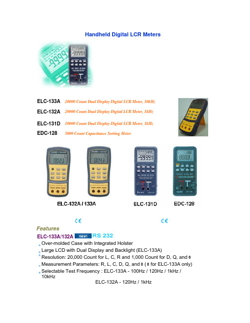
Handheld Digital LCR MetersELC-133A20000 Count Dual Display Digital LCR Meter, 10kHz ELC-132A20000 Count Dual Display Digital LCR Meter, 1kHz ELC-131D10000 Count Dual Display Digital LCR Meter, 1kHz EDC-1285000 Count Capacitance Sorting MeterFeaturesELC-133A/132AOver-molded Case with Integrated HolsterLarge LCD with Dual Display and Backlight (ELC-133A) Resolution: 20,000 Count for L, C, R and 1,000 Count for D, Q, and θMeasurement Parameters: R, L, C, D, Q, and θ (θ for ELC-133A only) Selectable Test Frequency : ELC-133A - 100Hz / 120Hz / 1kHz /10kHzELC-132A - 120Hz / 1kHzMeasurement Ranges :L: 2mH to 1,000H; C: 2,000pF to 10mF; R: 20Ω to 10MΩQ: .000 to 999 Auto; D: .000 to 999 Auto; θ: ± 90° Parallel and Serial Test ModeAuto and Manual Ranging0.5% Basic Accuracy for Resistance Measurement0.7% Basic Accuracy for Capacitance and Inductance Measurement Tolerance Mode: 1%, 5%, 10%, and 20%Max / Min / Avg Dynamic RecordingRelative Mode for Reading Correlation and Comparison Applications Auto Protective Fuse CheckSelf-Calibration for Calibrating the Meter's Internal Parameters as well as External Connector ResidualsPowered by Battery or External AC/DC AdapterAuto Power OffLow Battery IndicatorOptical RS-232 InterfaceCE MarkELC-131DLarge LCD with Dual DisplayResolution: 10,000 Count for L, C, R and 1,000 Count for D, Q Measurement Parameters: R, L, C, D, and QSelectable Test Frequency: 120Hz / 1kHzMeasurement Ranges: L: 1mH to 10,000H; C: 1,000pF to 10mF; R: 10Ω to 10MΩQ: .000 to 999 Auto; D: .000 to 999 AutoParallel and Serial Test ModeAuto and Manual Ranging0.5% Basic Accuracy for Resistance Measurement0.7% Basic Accuracy for Capacitance and Inductance Measurement Tolerance Mode: 1%, 5%, and 10%Max / Min / Avg Dynamic RecordingRelative Mode for Reading Correlation and Comparison Applications Auto Protective Fuse CheckSelf-Calibration for Calibrating the Meter's Internal Parameters as well as External Connector ResidualsPowered by Battery or External AC/DC AdapterAuto Power OffLow Battery IndicatorCE MarkEDC-128Large LCD with Dual DisplayResolution: 5,000 Count for Capacitance and 1000 Counts forTolerance (%)Measurement Parameters: R, L, C, D, and QWide Range from 500pF to 50mF with 0.1pF Best ResolutionAuto and Manual Ranging1% Basic AccuracyTolerance Mode: 1%, 5%, and 10%Max / Min Dynamic RecordingData Hold Function to Freeze Displayed ReadingsRelative Mode for Reading Correlation and ComparisonApplicationsPowered by Battery or External AC/DC AdapterAuto Power OffLow Battery IndicatorOptical RS-232 InterfaceCE MarkOrdering InformationELC-133A20,000 Count Dual Display LCR Meter with RS-232ELC-132A20,000 Count Dual Display LCR Meter with RS-232ELC-131D10,000 Count Dual Display LCR MeterEDC-1285,000 Count Capacitance Sorting Meter with RS-232 Standard AccessoriesOperator's ManualTL-23Test Leads with Alligator Clip9V Alkaline BatteryOptional AccessoriesCP-03PC Communication Software Packagewith RS-232 Cable (EDC-128)CP-09PC Communication Software PackageEA-55Power Adapter, 220VAC, 12V/50mA(ELC-133A/132A/131D)EA-112Power Adapter, 110VAC, 12V/50mA(ELC-133A/132A/131D)EC-170Soft Carrying CaseEC-230Square Soft Carrying Case TW-01 SMD Tweezers EC-600Long Soft Carrying CaseEH-80G Grey Protective Holster (for ELC-131D,EDC-128)TW-01SMD Tweezers。
MC13213资料

Freescale Semiconductor Technical DataFreescale reserves the right to change the detail specifications as may be required to permit improvements in the design of its products.Document Number: MC1321xRev. 0.0, 03/2006MC1321xPackage InformationCase 1664-0171-pin LGA [9x9 mm]Ordering InformationDevice Device MarkingPackage MC132********LGA MC132********LGA MC132********LGA MC13214113214LGA1See Table 1 for more details.1IntroductionThe MC1321x family is Freescale’s second-generation ZigBee platform which incorporates a low power 2.4 GHz radio frequency transceiver and an 8-bitmicrocontroller into a single 9x9x1 mm 71-pin LGA package. The MC1321x solution can be used for wireless applications from simple proprietary point-to-point connectivity to a complete ZigBee mesh network. The combination of the radio and a microcontroller in a small footprint package allows for a cost-effective solution.The MC1321x contains an RF transceiver which is an IEEE 802.15.4-compliant radio that operates in the 2.4 GHz ISM frequency band. The transceiver includes a low noise amplifier, 1mW nominal output power, PA with internal voltage controlled oscillator (VCO), integrated transmit/receive switch, on-board power supply regulation, and full spread-spectrum encoding and decoding.The MC1321x also contains a microcontroller based on the HCS08 Family of Microcontroller Units (MCU) and can provide up to 60KB of flash memory and 4KB of RAM. The onboard MCU allows the communicationsMC13211/212/213/214ZigBee ™- Compliant Platform - 2.4 GHz Low Power Transceiver for the IEEE ® 802.15.4 Standard plus MicrocontrollerContents1Introduction . . . . . . . . . . . . . . . . . . . . . . . . . . 12MC1321x Pin Assignment and Connections 83MC1321x Serial Peripheral Interface (SPI) . 144IEEE 802.15.4 Modem . . . . . . . . . . . . . . . . . . 165MCU . . . . . . . . . . . . . . . . . . . . . . . . . . . . . . . . 256System Electrical Specification . . . . . . . . . 467Application Considerations . . . . . . . . . . . . . 638Mechanical Diagrams . . . . . . . . . . . . . . . . . . 68stack and also the application to reside on the same system-in-package (SIP). The MC1321x family is organized as follows:•The MC13211 has 16KB of flash and 1KB of RAM and is an ideal solution for low cost, proprietary applications that require wireless point-to-point or star network connectivity. TheMC13211 combined with the Freescale Simple MAC (SMAC) provides the foundation forproprietary applications by supplying the necessary source code and application examples to get users started on implementing wireless connectivity.•The MC13212 contains 32K of flash and 2KB of RAM and is intended for use with the Freescale fully compliant 802.15.4 MAC. Custom networks based on the 802.15.4 standard MAC can be implemented to fit user needs. The 802.15.4 standard supports star, mesh and cluster treetopologies as well as beaconed networks.•The MC13213 contains 60K of flash and 4KB of RAM and is also intended for use with the Freescale fully compliant 802.15.4 MAC where larger memory is required. In addition, this device can support ZigBee applications that use a stack from 3rd party vendors.•The MC13214 is a fully compliant ZigBee platform. The MC13214 contains 60K of flash and 4KB of RAM and uses the Figure 8 Wireless ZigBee Stack (Z-stack) software. Applications can beadded to develop fully certified ZigBee products.Applications include, but are not limited to, the following:•Residential and commercial automation—Lighting control—Security—Access control—Heating, ventilation, air-conditioning (HV AC)—Automated meter reading (AMR)•Industrial Control—Asset tracking and monitoring—Homeland security—Process management—Environmental monitoring and control—HV AC—Automated meter reading•Health Care—Patient monitoring—Fitness monitoring1.1Ordering InformationTable 1 provides additional details about the MC1321x family.1.2General Platform Features•IEEE 802.15.4 standard compliant on-chip transceiver/modem —2.4GHz—16 selectable channels—Programmable output power •Multiple power saving modes•2V to 3.4V operating voltage with on-chip voltage regulators •-40°C to +85°C temperature range •Low external component count•Supports single 16 MHz crystal clock source operation or dual crystal operation •Support for SMAC, IEEE 802.15.4, and ZigBee software •9mm x 9mm x 1mm 71-pin LGATable 1. Orderable Parts DetailsDevice Operating Temp Range(TA.)Package Memory Options DescriptionMC13211-40° to 85° C LGA1KB RAM, 16KB Flash Intended for proprietary applications and Freescale Simple MAC (SMAC)MC13211R2-40° to 85° C LGATape and Reel 1KB RAM, 16KB Flash Intended for proprietary applications and Freescale Simple MAC (SMAC)MC13212-40° to 85° C LGA2KB RAM, 32KB Flash Intended for IEEE 802.15.4 compliant applications and Freescale 802.15.4 MACMC13212R2-40° to 85° C LGATape and Reel 2KB RAM, 32KB Flash Intended for IEEE 802.15.4 compliant applications and Freescale 802.15.4 MACMC13213-40° to 85° CLGA4KB RAM, 60KB FlashIntended for IEEE 802.15.4 compliant applications and Freescale 802.15.4 MAC.Also supports ZigBee applications that use a stack from a 3rd party vendor.MC13213R2-40° to 85° CLGATape and Reel 4KB RAM, 60KB FlashIntended for IEEE 802.15.4 compliant applications and Freescale 802.15.4 MAC.Also supports ZigBee applications that use a stack from a 3rd party vendor.MC13214-40° to 85° C LGA4KB RAM, 60KB Flash Intended for full ZigBee compliant applications using the F8 Wireless Z-StackMC13214R2-40° to 85° CLGATape and Reel4KB RAM, 60KB FlashIntended for full ZigBee compliant applications using the F8 Wireless Z-Stack1.3Microcontroller Features•Low voltage MCU with 40 MHz low power HCS08 CPU core•Up to 60K flash memory with block protection and security and 4K RAM—MC13211: 16KB Flash, 1KB RAM—MC13212: 32KB Flash, 2KB RAM—MC13213: 60KB Flash, 4KB RAM—MC13214: 60KB Flash, 4KB RAM with ZigBee Z-stack•Low power modes (Wait plus Stop2 and Stop3 modes)•Dedicated serial peripheral interface (SPI) connected internally to 802.15.4 modem•One 4-channel and one 1-channel 16-bit timer/pulse width modulator (TPM) module with selectable input capture, output capture, and PWM capability.•8-bit port keyboard interrupt (KBI)•8-channel 8-10-bit ADC•Two independent serial communication interfaces (SCI)•Multiple clock source options—Internal clock generator (ICG) with 243 kHz oscillator that has +/-0.2% trimming resolution and +/-0.5% deviation across voltage.—Startup oscillator of approximately 8 MHz—External crystal or resonator—External source from modem clock for very high accuracy source or system low-cost option •Inter-integrated circuit (IIC) interface.•In-circuit debug and flash programming available via on-chip background debug module (BDM)—Two comparator and 9 trigger modes—Eight deep FIFO for storing change-of-flow addresses and event-only data—Tag and force breakpoints—In-circuit debugging with single breakpoint•System protection features—Programmable low voltage interrupt (LVI)—Optional watchdog timer (COP)—Illegal opcode detection•Up to 32 MCU GPIO with programmable pullups1.4RF Modem Features•Fully compliant IEEE 802.15.4 transceiver supports 250 kbps O-QPSK data in 5.0 MHz channels and full spread-spectrum encode and decode•Operates on one of 16 selectable channels in the 2.4 GHz ISM band•-1 dBm to 0 dBm nominal output power, programmable from -27 dBm to +3 dBm typical•Receive sensitivity of <-92 dBm (typical) at 1% PER, 20-byte packet, much better than the IEEE 802.15.4 specification of -85 dBm•Integrated transmit/receive switch•Dual PA ouput pairs which can be programmed for full differential single-port or dual-port operation that supports an external LNA and/or PA.•Three low power modes for increased battery life•Programmable frequency clock output for use by MCU•Onboard trim capability for 16 MHz crystal reference oscillator eliminates need for external variable capacitors and allows for automated production frequency calibration •Four internal timer comparators available to supplement MCU timer resources•Supports both packet data mode and streaming data mode•Seven GPIO to supplement MCU GPIO1.5Software FeaturesFreescale provides a wide range of software functionality to complement the MC1321x hardware. There are three levels of application solutions:1.Simple proprietary wireless connectivity.er networks built on the IEEE 802.15.4 MAC standard.3.ZigBee-compliant network stack.1.5.1Simple MAC (SMAC)•Small memory footprint (about 3 Kbytes typical)•Supports point-to-point and star network configurations•Proprietary networks•Source code and application examples provided1.5.2IEEE 802.15.4-Compliant MAC•Supports star, mesh and cluster tree topologies•Supports beaconed networks•Supports GTS for low latency•Multiple power saving modes (idle doze, hibernate)1.5.3ZigBee-Compliant Network Stack•Supports ZigBee 1.0 specification•Supports star, mesh and tree networks•Advanced Encryption Standard (AES) 128-bit security1.6System Block DiagramFigure1 shows a simplified block diagram of the MC1321x solution.Figure1. MC1321x System Level Block Diagram1.7System Clock ConfigurationThe MC321x device allows for a wide array of system clock configurations:•Pins are provided for a separate external clock source for the CPU. The external clock source can by derived from a crystal oscillator or from an external clock source•Pins are provided for a 16 MHz crystal for the modem clock source (required)•The modem crystal oscillator frequency can be trimmed through programming to maintain the tight tolerances required by IEEE 802.15.4•The modem provides a CLKO programmable frequency clock output that can be used as an external source to the CPU. As a result, a single crystal system clock solution is possible •Out of reset, the MCU uses an internally generated clock (approximately 8-MHz) for start-up. This allows recovery from stop or reset without a long crystal start-up delay•The MCU contains an internal clock generator (which can be trimmed) that can be used to run the MCU for low power operation. This internal reference is approximately 243 kHzFigure2. MC1321x Single Crystal System Clock Structure2MC1321x Pin Assignment and Connections Figure3 shows the MC1321x pinout.2.1Pin DefinitionsTable2 details the MC1321x pinout and functionality.Table2. Pin Function DescriptionPin #Pin Name Type Description Functionality1PTA3/KBI1P3DigitalInput/Output MCU Port A Bit 3 / Keyboard Input Bit 32PTA4/KBI1P4DigitalInput/Output MCU Port A Bit 4 / Keyboard Input Bit 43PTA5/KBI1P5DigitalInput/Output MCU Port A Bit 5 / Keyboard Input Bit 54PTA6/KBI1P6DigitalInput/Output MCU Port A Bit 6 / Keyboard Input Bit 65PTA7/KBI1P7DigitalInput/Output MCU Port A Bit 7 / Keyboard Input Bit 76VDDAD Power Input MCU power supply to ATD Decouple to ground.7PTG0/BKGND/MS DigitalInput/Output MCU Port G Bit 0 /Background / Mode SelectPTG0 is output only. Pin is I/O when used as BDMfunction.8PTG1/XTAL DigitalInput/Output/Output MCU Port G Bit 1 / Crystaloscillator outputFull I/O when not used as clock source.9PTG2/EXTAL DigitalInput/Output/Input MCU Port G Bit 2 / Crystaloscillator inputFull I/O when not used as clock source.10CLKO Digital Output Modem Clock Output Programmable frequencies of:16 MHz, 8 MHz, 4 MHz, 2 MHz, 1 MHz, 62.5 kHz,32.786+ kHz (default),and 16.393+ kHz.11RESET DigitalInput/OutputMCU reset. Active low12PTC0/TXD2DigitalInput/Output MCU Port C Bit 0 / SCI2 TX data out13PTC1/RXD2DigitalInput/Output MCU Port C Bit 1/ SCI2 RX data in14PTC2/SDA1DigitalInput/Output MCU Port C Bit 1/ IIC bus data15PTC3/SCL1DigitalInput/Output MCU Port C Bit 1/ IIC bus clock16PTC4DigitalInput/OutputMCU Port C Bit 417PTC5DigitalInput/OutputMCU Port C Bit 518PTC6DigitalInput/OutputMCU Port C Bit 619PTC7DigitalInput/OutputMCU Port C Bit 720PTE0/TXD1DigitalInput/Output MCU Port E Bit 0 / SCI1 TX data out21PTE1/RXD1DigitalInput/Output MCU Port E Bit 1/ SCI1 RX data in22VDDD Power Output Modem regulated outputsupply voltageDecouple to ground.23VDDINT Power Input Modem digital interfacesupply 2.0 to 3.4 V. Decouple to ground. Connect to Battery.24GPIO5DigitalInput/Output Modem General Purpose Input/Output 525GPIO6DigitalInput/Output Modem General Purpose Input/Output 626GPIO7DigitalInput/Output Modem General Purpose Input/Output 727XTAL1Input Modem crystal referenceoscillator inputConnect to 16 MHz crystal and load capacitor.28XTAL2Input/Output Modem crystal referenceoscillator output Connect to 16 MHz crystal and load capacitor. Do not load this pin by using it as a 16 MHz source. Measure 16 MHz output at CLKO, programmed for 16 MHz.29VDDLO2Power Input Modem LO2 VDD supply Connect to VDDA externally.30VDDLO1Power Input Modem LO1 VDD supply Connect to VDDA externally.31VDDVCO Power Output Modem VCO regulatedsupply bypassDecouple to ground.32VBATT Power Input Modem voltage regulators’inputDecouple to ground. Connect to Battery.33VDDA Power Output Modem analog regulatedsupply output Decouple to ground. Connect to directly VDDLO1 and VDDLO2 externally and to PAO_P andPAO_M through a bias network.34CT_Bias RF ControlOutput Modem biasvoltage/control signal forRF external componentsWhen used with internal T/R switch, providesground reference for RX and VDDA reference forTX. Can also be used as a control signal withexternal LNA, antenna switch, and/or PA.35RFIN_M RF Input(Output)Modem RF input/outputnegativeWhen used with internal T/R switch, this is abi-directional RF port for the internal LNA and PA36RFIN_P RF Input(Output)Modem RF input/outputpositiveWhen used with internal T/R switch, this is abi-directional RF port for the internal LNA and PATable2. Pin Function Description (continued)Pin #Pin Name Type Description Functionality37NC Not used May be grounded or left open38PAO_P RF Output Modem power amplifierRF output positive Open drain. Connect to VDDA through a bias network when used with external balun. Not used when internal T/R switch is used.39PAO_M RF Output Modem power amplifierRF output negative Open drain. Connect to VDDA through a bias network when used with external balun. Not used when internal T/R switch is used.40SM Input Test Mode pin Must be grounded for normal operation41GPIO4DigitalInput/Output Modem General Purpose Input/Output 442GPIO3DigitalInput/Output Modem General Purpose Input/Output 343GPIO2Test Point MCU Port E Bit 6 / ModemGeneral PurposeInput/Output 2Internally connected pins. When gpio_alt_en, Register 9, Bit 7 = 1, GPIO2 functions as a “CRC Valid” indicator.44GPIO1Test Point MCU Port E Bit 7 / ModemGeneral PurposeInput/Output 1Internally connected pins. When gpio_alt_en, Register 9, Bit 7 = 1, GPIO1 functions as an “Out of Idle” indicator.45VDD Power Input MCU main power supply Decouple to ground.46ATTN Test Point MCU Port D Bit 0 / Modemattention inputInternally connected pins.47PTD2/TPM1CH2DigitalInput/Output MCU Port D Bit 2 / TPM1 Channel 248PTD4/TPM2CH1DigitalInput/Output MCU Port D Bit 4 / TPM2 Channel 149PTD5/TPM2CH2DigitalInput/Output MCU Port D Bit 5 / TPM2 Channel 250PTD6/TPM2CH3DigitalInput/Output MCU Port D Bit 6 / TPM2 Channel 351PTD7/TPM2CH4DigitalInput/Output MCU Port D Bit 7 / TPM2 Channel 452PTB0/AD1P0Input/Output MCU Port B Bit 0 / ATDanalogChannel 053PTB1/AD1P1Input/Output MCU Port B Bit 1 / ATDanalog Channel 154PTB2/AD1P2Input/Output MCU Port B Bit 2 / ATDanalog Channel 255PTB3/AD1P3Input/Output MCU Port B Bit 3 / ATDanalog Channel 356PTB4/AD1P4Input/Output MCU Port B Bit 4 / ATDanalog Channel 4Pin #Pin Name Type Description Functionality57PTB5/AD1P5Input/Output MCU Port B Bit 5 / ATDanalog Channel 558PTB6/AD1P6Input/Output MCU Port B Bit 6 / ATDanalog Channel 659PTB7/AD1P7Input/Output MCU Port B Bit 7 / ATDanalog Channel 760VREFH Input MCU high referencevoltage for ATD61VREFL Input MCU low referencevoltage for ATD62PTA0/KBI1P0DigitalInput/Output MCU Port A Bit 0 / Keyboard Input Bit 063PTA1/KBI1P1DigitalInput/Output MCU Port A Bit 1 / Keyboard Input Bit 164PTA2/KBI1P2DigitalInput/Output MCU Port A Bit 2 / Keyboard Input Bit 265TEST Test Point For factory test Do not connect 66TEST Test Point For factory test Do not connect 67TEST Test Point For factory test Do not connect 68TEST Test Point For factory test Do not connect 69TEST Test Point For factory test Do not connect 70TEST Test Point For factory test Do not connect 71TEST Test Point For factory test Do not connectFLAG VSS Power input External package flag.Common VSS Connect to ground.Pin #Pin Name Type Description Functionality2.2Internal Functional InterconnectsThe MCU provides control for the 802.15.4 modem. The required interconnects between the devices are routed onboard the SiP. In addition, the signals are brought out to external pads primarily for use as test points. These signals can be useful when writing and debugging software.Table3. Internal Functional InterconnectsPin #MCU Signal Modem Signal Description43PTE6GPIO2Modem GPIO2 output acts as “CRC Valid” status indicator for Stream DataMode to MCU.44PTE7GPIO1Modem GPIO1 output acts as “Out of Idle” status indicator for Stream DataMode to MCU.46PTD0ATTN MCU Port D Bit 0 drives the attention (ATTN) input of the modem to wakemodem from Hibernate or Doze Mode.PTE5/SPSCK1SPICLK MCU SPI master SPI clock output drives modem SPICLK slave clock input.PTE4/MOSI1MOSI MCU SPI master MOSI output drives modem slave MOSI inputPTE3/MISO1MISO Modem SPI slave MISO output drives MCU master MISO inputPTE2/SS1CE MCU SPI master SS output drives modem slave CE inputIRQ M_IRQ Modem interrupt request M_IRQ output drives MCU IRQ inputPTD1RXTXEN MCU Port D Bit 1 drives the RXTXEN input to the modem to enable TX or RXor CCA operations.PTD3M_RST MCU Port D Bit 3 drives the reset M_RST input to the modem.NOTETo use the MCU and modem signals as described in Table3, the MCU needsto be programmed appropriately for the stated function.3MC1321x Serial Peripheral Interface (SPI)The MC1321x modem and CPU communicate primarily through the onboard SPI command channel. Figure4 shows the SiP internal interconnects with the SPI bus highlighted. The MCU has a single SPI module that is dedicated to the modem SPI interface. The modem is a slave only and the MCU SPI must be programmed and used as a master only. Further, the SPI performance is limited by the modem constraints of 8 MHz SPI clock frequency, and use of the SPI must be programmed to meet the modem SPI protocol.3.1SiP Level SPI Pin ConnectionsThe SiP level SPI pin connections are all internal to the device. Figure4 shows the SiP interconnections with the SPI bus highlighted.Figure4. MC1321x Internal Interconnects Highlighting SPI BusTable4. MC1321x Internal SPI ConnectionsMCU Signal Modem Signal DescriptionPTE5/SPSCK1SPICLK MCU SPI master SPI clock output drives modem SPICLK slave clock input.PTE4/MOSI1MOSI MCU SPI master MOSI output drives modem slave MOSI inputPTE3/MISO1MISO Modem SPI slave MISO output drives MCU master MISO inputPTE2/SS1CE MCU SPI master SS output drives modem slave CE input3.2SPI Features•MCU bus master •Modem bus slave•Programmable SPI clock rate; maximum rate is 8 MHz •Double-buffered transmit and receive at MCU•Serial clock phase and polarity must meet modem requirements (MCU control bits •Slave select programmed to meet modem protocol3.3SPI System Block DiagramFigure 5 shows the SPI system level diagram.Figure 5. SPI System Block DiagramFigure 5 shows the SPI modules of the MCU and modem in the master-slave arrangement. The MCU (master) initiates all SPI transfers. During a transfer, the master shifts data out (on the MOSI pin) to the slave while simultaneously shifting data in (on the MISO pin) from the slave. Although the SPI interface supports simultaneous data exchange between master and slave, the modem SPI protocol only uses data exchange in one direction at a time. The SPSCK signal is a clock output from the master and an input to the slave. The slave device must be selected by a low level on the slave select input (SS1 pin).7654321SPI SHIFTERCLOCK GENERATOR7654321SPI SHIFTER PTE2/SS1SPSCK1MISO1MOS1CESPICLKMISOMOSIMCU (MASTER)MODEM (SLAVE)4IEEE 802.15.4 Modem4.1Block DiagramFigure6. 802.15.4 Modem Block Diagram4.2Data Transfer ModesThe 802.15.4 modem has two data transfer modes:1.Packet Mode — Data is buffered in on-chip RAM2.Streaming Mode — Data is processed word-by-wordThe Freescale 802.15.4 MAC software only supports the streaming mode of data transfer. For proprietary applications, packet mode can be used to conserve MCU resources.4.3Packet StructureFigure7 shows the packet structure of the 802.15.4 modem. Payloads of up to 125 bytes are supported. The 802.15.4 modem adds a four-byte preamble, a one-byte Start of Frame Delimiter (SFD), and aone-byte Frame Length Indicator (FLI) before the data. A Frame Check Sequence (FCS) is calculated and appended to the end of the data.4 bytes 1 byte 1 byte125 bytes maximum 2 bytesPreamble SFD FLI Payload Data FCSFigure7. 802.15.4 modem Packet Structure4.4Receive Path DescriptionIn the receive signal path, the RF input is converted to low IF In-phase and Quadrature (I & Q) signals through two down-conversion stages. A Clear Channel Assessment (CCA) can be performed based upon the baseband energy integrated over a specific time interval. The digital back end performs Differential Chip Detection (DCD), the correlator “de-spreads” the Direct Sequence Spread Spectrum (DSSS) Offset QPSK (O-QPSK) signal, determines the symbols and packets, and detects the data.The preamble, SFD, and FLI are parsed and used to detect the payload data and FCS (which are stored in RAM in Packet Mode). A two-byte FCS is calculated on the received data and compared to the FCS value appended to the transmitted data, which generates a Cyclical Redundancy Check (CRC) result. A parameter of received energy during the reception called the Link Quality Indicator is measured over a 64 µs period after the packet preamble and stored in an SPI register.If the 802.15.4 modem is in Packet Mode, the data is stored in RAM and processed as an entire packet. The MCU is notified that an entire packet has been received via an interrupt.If the 802.15.4 modem is in streaming mode, the MCU is notified by a recurring interrupt on aword-by-word basis.Figure8 shows CCA reported power level versus input power. Note that CCA reported power saturates at about -57 dBm input power which is well above IEEE 802.15.4 Standard requirements. Figure9 shows energy detection/LQI reported level versus input power.NOTEFor both graphs, the required IEEE 802.15.4 Standard accuracy and rangelimits are shown. A 3.5 dBm offset has been programmed into the CCAreporting level to center the level over temperature in the graphs.FigureFigure4.5For the transmit path, the TX data that was previously written to the internal RAM is retrieved (packet mode) or the TX data is clocked in via the SPI (stream mode), formed into packets per the 802.15.4 PHY, spread, and then up-converted to the transmit frequency.If the 802.15.4 modem is in packet mode, data is processed as an entire packet. The data is first loaded into the TX buffer. The MCU then requests that the modem transmit the data. The MCU is notified via an interrupt when the whole packet has successfully been transmitted.In streaming mode, the data is fed to the 802.15.4 modem on a word-by-word basis with an interrupt serving as a notification that the 802.15.4 modem is ready for more data. This continues until the whole packet is transmitted.In both modes, a two-byte FCS is calculated in hardware from the payload data and appended to the packet. This done without intervention from the user.4.6Functional Description4.6.1802.15.4 Modem Operational ModesThe 802.15.4 modem has a number of operational modes that allow for low-current operation. Transition from the Off to Idle mode occurs when M_RST is negated. Once in Idle, the SPI is active and is used to control the IC. Transition to Hibernate and Doze modes is enabled via the SPI. These modes aresummarized, along with the transition times, in Table 5. Current drain in the various modes is listed in Table 8, DC Electrical Characteristics.4.6.2Serial Peripheral Interface (SPI)The MCU directs the 802.15.4 modem, checks its status, and reads/writes data to the device through the 4-wire SPI port. The transceiver operates as a SPI slave device only. A transaction between the host and the 802.15.4 modem occurs as multiple 8-bit bursts on the SPI. The modem SPI signals are:1.Chip Enable (CE) - A transaction on the SPI port is framed by the active low CE input signal. Atransaction is a minimum of 3 SPI bursts and can extend to a greater number of bursts.2.SPI Clock (SPICLK) - The host drives the SPICLK input to the 802.15.4 modem. Data is clockedinto the master or slave on the leading (rising) edge of the return-to-zero SPICLK and data out changes state on the trailing (falling) edge of SPICLK.Table 5. 802.15.4 Modem Mode Definitions and Transition TimesMode DefinitionTransition Time To or From IdleOff All IC functions Off, Leakage only. M_RST asserted. Digital outputs are tri-stated including IRQ10 - 25 ms to Idle Hibernate Crystal Reference Oscillator Off. (SPI not functional.) IC Responds to ATTN. Data is retained.7 - 20 ms to Idle DozeCrystal Reference Oscillator On but CLKO output available only if Register 7, Bit 9 = 1 for frequencies of 1 MHz or less. (SPI not functional.) Responds to ATTN and can be programmed to enter Idle Mode through an internal timer comparator. (300 + 1/CLKO) µs to Idle Idle Crystal Reference Oscillator On with CLKO output available. SPI active.Receive Crystal Reference Oscillator On. Receiver On.144 µs from Idle TransmitCrystal Reference Oscillator On. Transmitter On.144 µs from IdleNOTEFor the MCU, the SPI clock format is the clock phase control bit CPHA = 0and the clock polarity control bit CPOL = 0.3.Master Out/Slave In (MOSI) - Incoming data from the host is presented on the MOSI input.4.Master In/Slave Out (MISO) - The 802.15.4 modem presents data to the master on the MISOoutput.Although the SPI port is fully static, internal memory, timer and interrupt arbiters require an internal clock (CLK core), derived from the crystal reference oscillator, to communicate from the SPI registers to internal registers and memory.4.6.2.1SPI Burst OperationThe SPI port of the MCU transfers data in bursts of 8 bits with most significant bit (MSB) first. The master (MCU) can send a byte to the slave (transceiver) on the MOSI line and the slave can send a byte to the master on the MISO line. Although an 802.15.4 modem transaction is three or more SPI bursts long, the timing of a single SPI burst is shown in Figure10. The maximum SPI clock rate is 8 Mhz from the MCU because the modem is limited by this number.。
JMDM-14DIO 控制器说明书
JMDM系列产品说明书-14DIO 深圳市精敏数字机器有限公司JMDM-14DIO控制器说明书一、特性1、8位高性能单片机作为主控制芯片,6倍于普通单片机的速度;2、主电源:交流9V,或直流12V。
3、8路光电隔离数字量输入,NPN输入形式,输入电流为10mA;4、6路光电隔离数字量输出:其中有4路是继电器隔离输出,可以直接接220V工作电压,最大输出电流为4A; 2路是光电隔离晶体管输出,用于高频场合,最大输出电流为1A,可以控制步进电机和伺服电机,输出频率可以达到40KHz,也可作为PWM应用;5、有一路标准的RS232串口通信接口,可以与电脑等上位软件通信,也可以与多个控制器之间联机工作;6、可直接通过RS232接口下载程序,无需烧录器,方便程序修改、升级;7、512字节的数据存储器,可以用来保存参数等数据,断电数据不丢失;8、系统采用光电隔离和启用内部看门狗及严格的高频滤除特性,使系统工作稳定可靠,无死机现象;9、内部电路板尺寸为92mm*86mm,对于安装空间比较小的场合可以不装外壳,特别适合小型机械的应用;10、紧凑型机壳,控制器机壳尺寸:115mm*100mm,可用螺钉安装或导轨安装;11、用Keil C 或汇编编程,用户编程有困难的可把工艺流程发给我司,我司可帮助编程。
二、规格1、工作温度:-10~+65°C;2、储存温度:-20~+80°C ;3、湿度:5~95% 无凝结;4、功耗(无外部设备):+*******(典型值) ;三、用途1、可用于各种14个点以内的控制系统,可控制气缸,电磁阀,继电器,步进电机,可外接光电式,电容式,电感式,霍尔式等各种传感器;2、可用于替代14点以内的PLC用于各种控制场合(如各种机器控制);3、可用于单片机学习和试验。
四、订购信息及售后服务订购信息:JMDM-14DIO控制器1台、RS232串口通信下载线1条(附送)、光盘(包括编程软件、教程、应用范例、说明书文档)、说明书;发货方式:快递。
MCD3000产品介绍

MCD3000产品介绍丹佛斯软启动器MCD3000系列完美的软启动,保护及操作方便产品范围:7.5 - 800 kW主要功能:电流额定值适用于正常启动和重负载启动提供有 200-690 VAC 的型号通过内部电流斜坡上升实现电流极限软启动四种不同的、可自动调整的斜坡下降配置众多电动机保护功能内置本地控制面板(带显示屏)对参数实行密码保护直流制动功能:交流保护/过流保护——防止泵类空载/过载相序保护——防止意外反向运转电网失衡保护电机保护功能——旁路运行时的电机保护工作原理:电机电压是受相位分割原理控制的。
每个相位中的两个闸流体执行电源转换,能使起动装置处理高的起动转矩及经常性的起动和关闭。
电流变压器测定电机电流,为电机起动的恒定电流控制提供反馈,同时也为许多电机保护及应和保护功能提供反馈。
安装方便:MCD3000软启动装置可靠墙安装,为电缆密封和封端留出足够的空间;并行安装无间隙(较大的规格只有100mm的间隙);在控制电机时,不需增加任何其它设备。
操作方便:在基本操作中,只需调整一下参数;在高水平控制和保护时,只需调整几个参数;不需现场校准即可正确运转,MCD3000的电流测定量达±5%的精度;有带显示屏的本地控制器。
MCD3000软起动装置为电机和设备操作提供许多优点,其中包括: 灵活控制起动电流和转矩;平稳控制电流和电压,无跳动和不稳定过程;频繁的起/停,无机械损坏现象;适应起动的各种变化,增加了应用的灵活性;软停止控制,延长电机寿命;制动控制,延长电机寿命。
型号功率MCD3007-T5-B21-CV4 7.5KWMCD3015-T5-B21-CV4 15KWMCD3018-T5-B21-CV4 18.5KWMCD3022-T5-B21-CV4 22KWMCD3030-T5-B21-CV4 30KWMCD3037-T5-B21-CV4 37KWMCD3045-T5-B21-CV4 45KWMCD3055-T5-B21-CV4 55KW MCD3075-T5-C21-CV4 75KW MCD3090-T5-C21-CV4 90KW MCD3110-T5-C21-CV4 110KW MCD3132-T5-C21-CV4 132KW MCD3185-T5-C20-CV4 185KW MCD3220-T5-C20-CV4 220KW MCD3300-T5-C20-CV4 300KW MCD3315-T5-C20-CV4 315KW MCD3400-T5-C20-CV4 400KW MCD3500-T5-C20-CV4 500KW MCD3600-T5-C20-CV4 600KW MCD3700-T5-C20-CV4 700KW MCD3800-T5-C20-CV4 800KW MCD3007T5B21CV4 175G5002 MCD3007T7B21CV4 175G5003 MCD3015T5B21CV4 175G5006 MCD3015T7B21CV4 175G5007 MCD3018T5B21CV4 175G5010 MCD3018T7B21CV4 175G5011 MCD3022T5B21CV4 175G5014 MCD3022T7B21CV4 175G5015 MCD3030T5B21CV4 175G5018 MCD3030T7B21CV4 175G5019MCD3037T5B21CV4 175G5022 MCD3037T7B21CV4 175G5023 MCD3045T5B21CV4 175G5026 MCD3045T7B21CV4 175G5027 MCD3055T5B21CV4 175G5030 MCD3055T7B21CV4 175G5031 MCD3075T5C21CV4 175G5034 MCD3075T7C21CV4 175G5035 MCD3090T5C21CV4 175G5038 MCD3090T7C21CV4 175G5039 MCD3110T5C21CV4 175G5042 MCD3110T7C21CV4 175G5043 MCD3132T5C21CV4 175G5046 MCD3132T7C21CV4 175G5047 MCD3185T5C20CV4 175G5050 MCD3185T7C20CV4 175G5051 MCD3220T5C20CV4 175G5054 MCD3220T7C20CV4 175G5055 MCD3300T5C20CV4 175G5058 MCD3300T7C20CV4 175G5059 MCD3315T5C20CV4 175G5062 MCD3315T7C20CV4 175G5063 MCD3400T5C20CV4 175G5066 MCD3400T7C20CV4 175G5067 MCD3500T5C20CV4 175G5070 MCD3500T7C20CV4 175G5071 MCD3600T5C20CV4 175G5074 MCD3600T7C20CV4 175G5075 MCD3700T5C20CV4 175G5078 MCD3700T7C20CV4 175G5079 MCD3800T5C20CV4 175G5082 MCD3800T7C20CV4 175G5083。
- 1、下载文档前请自行甄别文档内容的完整性,平台不提供额外的编辑、内容补充、找答案等附加服务。
- 2、"仅部分预览"的文档,不可在线预览部分如存在完整性等问题,可反馈申请退款(可完整预览的文档不适用该条件!)。
- 3、如文档侵犯您的权益,请联系客服反馈,我们会尽快为您处理(人工客服工作时间:9:00-18:30)。
I TRMS =2x 300 A I TAVM =2x 130 A V RRM =800-1800 VSymbol Test Conditions Maximum RatingsI TRMS , I FRMS T VJ = T VJM300A I TAVM , I FAVM T C = 85°C; 180° sine 130A I TSM , I FSMT VJ = 45°C;t = 10 ms (50 Hz), sine 4750A V R = 0t = 8.3 ms (60 Hz), sine 5080A T VJ = T VJM t = 10 ms (50 Hz), sine 4230A V R = 0t = 8.3 ms (60 Hz), sine 4530A òi 2dtT VJ = 45°C t = 10 ms (50 Hz), sine 113 000A 2s V R = 0t = 8.3 ms (60 Hz), sine 108 000A 2s T VJ = T VJM t = 10 ms (50 Hz), sine 89 500A 2s V R = 0t = 8.3 ms (60 Hz), sine86 200A 2s (di/dt)crT VJ = T VJM repetitive, I T = 500 A 150A/m sf =50 Hz, t P =200 m s V D = 2/3 V DRM I G = 0.5 A non repetitive, I T = 500 A 500A/m s diG /dt = 0.5 A/m s(dv/dt)cr T VJ = T VJM ;V DR = 2/3 V DRM1000V/m s R GK = ¥; method 1 (linear voltage rise)P GM T VJ = T VJM t P =30 m s 120W I T = I TAVMt P =500 m s60W P GAV 8W V RGM 10V T VJ -40...+125°C T VJM 125°C T stg -40...+125°C V ISOL 50/60 Hz, RMS t = 1 min 3000V~I ISOL £ 1 mAt = 1 s 3600V~M d Mounting torque (M6)2.25-2.75/20-25Nm/lb.in.Terminal connection torque (M6) 4.5-5.5/40-48Nm/lb.in.WeightTypical including screws125gV RSM V RRM Type V DSM V DRM V V Version 1Version 1900800MCC 132-08io1MCD 132-08io113001200MCC 132-12io1MCD 132-12io115001400MCC 132-14io1MCD 132-14io117001600MCC 132-16io1MCD 132-16io119001800MCC 132-18io1MCD 132-18io1Data according to IEC 60747 and refer to a single thyristor/diode unless otherwise stated.IXYS reserves the right to change limits, test conditions and dimensionsFeaturesq International standard packageq Direct copper bonded Al 2O 3 -ceramic base plateq Planar passivated chips q Isolation voltage 3600 V~q UL registered, E 72873qKeyed gate/cathode twin pinsApplications q Motor control q Power converterq Heat and temperature control for industrial furnaces and chemical processesq Lighting controlqContactless switchesAdvantagesq Space and weight savings q Simple mountingqImproved temperature and power cyclingqReduced protection circuitsThyristor ModulesThyristor/Diode ModulesMCDMCC315421236754032Symbol Test ConditionsCharacteristic ValuesIRRM , I DRM T VJ = T VJM ; V R = V RRM ; V D = V DRM 10mA V T , V F I T , I F = 300 A; T VJ = 25°C1.36V V T0For power-loss calculations only (T VJ = 125°C)0.8V r T 1.5m W V GT V D = 6 V;T VJ = 25°C2.5V T VJ = -40°C 2.6V I GT V D = 6 V;T VJ = 25°C 150mA T VJ = -40°C 200mA V GD T VJ = T VJM ;V D = 2/3 V DRM0.2V I GD 10mA I L T VJ = 25°C; t P = 30 m s; V D = 6 V 300mA I G = 0.5 A; di G /dt = 0.5 A/m s I H T VJ = 25°C; V D = 6 V; R GK = ¥200mA t gd T VJ = 25°C; V D = 1/2 V DRM 2m s I G = 0.5 A; di G /dt = 0.5 A/m st q T VJ = T VJM ; I T = 160 A, t P = 200 m s; -di/dt = 10 A/m s typ.150m s V R = 100 V; dv/dt = 20 V/m s; V D = 2/3 V DRM Q S T VJ = T VJM ; I T , I F = 300 A, -di/dt = 50 A/m s 550m C I RM 235A R thJC per thyristor/diode; DC current 0.23K/W per moduleother values 0.115K/W R thJK per thyristor/diode; DC current see Fig. 8/90.33K/W per module0.165K/W d S Creepage distance on surface 12.7mm d A Strike distance through air9.6mm aMaximum allowable acceleration50m/s 2Optional accessories for modulesKeyed gate/cathode twin plugs with wire length = 350 mm, gate = yellow, cathode = red Type ZY 180L (L = Left for pin pair 4/5)UL 758, style 1385,Type ZY 180R (R = right for pin pair 6/7)CSA class 5851, guide 460-1-1Dimensions in mm (1 mm = 0.0394")MCCMCDFig. 1 Gate trigger characteristicsFig. 2 Gate trigger delay timeFig. 4i 2t versus time (1-10 ms)Fig. 4a Maximum forward currentat case temperature Fig. 5Power dissipation versus on-state current and ambient temperature (per thyristor or diode)Fig. 6Three phase rectifier bridge:Power dissipation versus direct output current and ambient temperatureFig. 3Surge overload currentI TSM , I FSM : Crest value, t: durations tms t0.0010.010.1101000200030004000110104105106A 2s I TSMA i 2tT VJ = 45°CT VJ = 125°C80 % V RRM T VJ = 45°C 50 HzT VJ = 125°CFig. 7Three phase AC-controller:Power dissipation versus RMS output current and ambient temperatureFig. 8Transient thermal impedancejunction to case (per thyristor or diode)Fig. 9Transient thermal impedancejunction to heatsink (per thyristor or diode)R thJC for various conduction angles d: d R thJC (K/W) DC 0.230180°0.244120°0.25560°0.28330°0.321Constants for Z thJC calculation:i R thi (K/W)t i (s)10.00950.00120.01750.06530.2030.4RthJK for various conduction angles d: d R thJK (K/W) DC 0.330180°0.344120°0.35560°0.38330°0.421Constants for Z thJK calculation:i R thi (K/W)t i (s)10.00950.00120.01750.06530.2030.440.11.29。