51.2 A New Low Power PMOS Poly-Si Inverter and Driving Circuits
AMOLED-LTPS-OLED介绍

Seal & Encapsulation
Module Process
Evaluation Process
Driver IC Attachment
FPC
일반
17 /56
TFT Process
일반
18 /56
Silicon Material
a-Si:H Poly Si Single Si
Crystallization
New a-Si & gate oxide New structure & Circuit
일반
20 /56
TFT Issue - ELA LTPS TFT
Merits & Demerits
ELA-LTPS TFT AMOLED W/S
Good Stability of TFT Circuit Integration Possibility of PMOS TFT Low Uniformity of Transistor High investment and Process cost Low scalability (Gen. 4)
Total Material Cost : 85.5%
BLU Pol.
BLU
Pol. C/F Glass+Encap
basically low material cost
C/F 30.3% Glass 7.6% Ref : SDI (’06.1)
일반
14 /56
AMOLED Development History
STN TFT OLED
50% Mobile Display Div.
Sub-1V CMOS Voltage Reference Based on Weighted Vgs
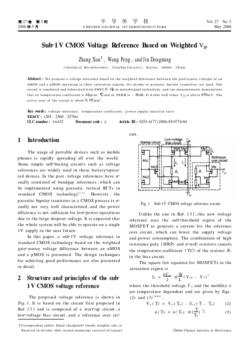
cuit .
1 Introduction
The usage of portable devices such as mo bile p ho nes is rapidly sp reading all over t he world. So me simple self2biasing circuit s such as voltage references are widely used in t hese bat tery2opera2 ted devices. In t he past ,voltage references have u2 sually co nsisted of bandgap references , which can be implemented using parasitic vertical BJ Ts in standard CMOS technology [ 1 ,2 ] . However , t he parasitic bipolar t ransistor in a CMOS p rocess is u2 sually not very well characterized , and t he power efficiency is not sufficient for low2power operatio ns due to t he large dropo ut voltage. It is expected t hat t he whole system will be able to operate o n a single 1V supply in t he near f ut ure. In t his paper , a sub21V voltage reference in standard CMOS technology based o n t he weighted gate2so urce voltage difference bet ween an nMOS and a p MOS is p resented. The design techniques for achieving good performance are al so p resented in detail .
MEMS 实验 使用L-Edit画PMOS布局图
XXXXXXXX大学(MEMS)实验报告实验名称使用 L-Edit 画PMOS 布局图实验时间年月日专业姓名学号预习操作座位号教师签名总评一、实验目的:1、熟悉版图设计工具L-Edit的使用方法,并且能正确的使用这些工具;2、掌握版图设计的设计规则;3、能运用L-Edit 实现器件的布局图,以PMOS与NMOS设计为例;二、基本原理:1、CMOS器件的制作工艺2、PMOS器件和NMOS器件的版图实验原理截图:(1)PMO版图设计原理图:(2)CMOS版图设计原理图:3、设计版图时的注意事项:(1)L-Edit编辑环境是预设在P型基板上,故在P型基板上制作PMOS的第一步是需要做出N Well区,即需设定N阱区;然而对于NMOS则不需要N Well群区。
此外在设计版图时,需要将图绘制在原点之上,否则不利用版图截面的观察。
(2)改变图形大小的方法:“alt+鼠标拖动边框”;移动图形的方法“alt+鼠标拖动图形”;(3)绘制各图层之前需先通过Tools---DRC Setup查看对应的设计规则,从而选择确定图层的大小;绘制完一个图层都需DRC 进行设计规则检查;(4)各图层绘制无先后顺序的规定;(5)绘图时可适当使用“尺子”功能,以确保版图设计的对称性;清除图中的“尺寸”使用“View---Objects---Rules”或者选中后删除。
(6)对版图设计时,要注意时刻遵循设计规则,否则会出错误。
(7)对版图进行截面观察时,应注意选择好文件的路径,并且要设置好适当的界线位置。
三、实验内容及步骤:(1)打开 L-Edit 程序。
(2)另存新文件:选择 File---Save As命令,打开“另存为”对话框,在“保存在”下拉列表框中选择存储目录,在“文件名”文本框中输入新文件名称,例如:exp3。
(3)取代设定:选择File---Replace Setup命令,单击出现的对话框的From file 下拉列表右侧的 Browser按钮,择…:\LEdit83\Samples\SPR\example1\lights.tdb文件,再单击 OK 按钮,就可将 lights.tdb 文件的设定选择性应用在目前编辑的文件,包括格点设定、图层设定等。
5 V pMOS器件的热载流子注入退化机理

5 V pMOS器件的热载流子注入退化机理杨翰琪;刘小红;吕康;魏家行;孙伟锋【摘要】研究了低压pMOS器件热载流子注入HCI(Hot-Carrier Injection)退化机理,分析了不同的栅压应力下漏极饱和电流(Idsat)退化出现不同退化趋势的原因.结合实测数据并以实际样品为模型进行了器件仿真,研究表明,快界面态会影响pMOS器件迁移率,导致Idsat的降低;而电子注入会降低pMOS器件阈值电压(Vth),导致Idsat的上升.当栅压为-7.5 V时,界面态的产生是导致退化的主要因素,在栅压为-2.4 V的应力条件下,电子注入在热载流子退化中占主导作用.【期刊名称】《电子器件》【年(卷),期】2018(041)005【总页数】4页(P1093-1096)【关键词】pMOS;热载流子注入;不同栅压应力;TCAD仿真【作者】杨翰琪;刘小红;吕康;魏家行;孙伟锋【作者单位】东南大学国家专用集成电路系统工程技术研究中心,南京210096;华润上华半导体有限公司,江苏无锡214000;华润上华半导体有限公司,江苏无锡214000;东南大学国家专用集成电路系统工程技术研究中心,南京210096;东南大学国家专用集成电路系统工程技术研究中心,南京210096【正文语种】中文【中图分类】TN386.1随着集成电路制造工艺迅速向深亚微米、超深亚微米方向不断发展,热载流子效应已经成为限制器件与电路的寿命及可靠性的主要因素之一[1-2]。
目前,对MOS器件的热载流子退化研究主要是针对n型金属氧化物半导体晶体管(nMOSFET)。
由于在相同电场中迁移率小的空穴获得的动能远小于迁移率大的电子,所以在相同电压偏置下,p型金属氧化物半导体晶体管(pMOSFET)中热空穴引起的器件损伤远小于nMOS器件中热电子引起的器件损伤,因此pMOS器件的热载流子退化的研究一直为人们所忽视[3-5]。
但随着器件尺寸进入亚微米和深亚微米范围,pMOS器件的热载流子退化变得越来越严重,已成为CMOS电路退化以及失效不可忽视的因素,所以对pMOS器件的热载流子退化进行深入研究是十分必要的。
一种常温下聚苯乙烯微流控芯片的制备方法(英文)
Sensors and Actuators B 248(2017)311–317Contents lists available at ScienceDirectSensors and Actuators B:Chemicalj o u r n a l h o m e p a g e :w w w.e l s e v i e r.c o m /l o c a t e /s nbSilicon based solvent immersion imprint lithography for rapid polystyrene microfluidic chip prototypingJingdong Chen a ,∗,Wenjie Wang a ,Weibang Ji a ,Shaoding Liu a ,Qiushu Chen b ,Bimin Wu b ,Rhima Coleman b ,Xudong Fan a ,b ,∗aKey Lab of Advanced Transducers and Intelligent Control System,Ministry of Education and Shanxi Province,College of Physics and Optoelectronics,Taiyuan University of Technology,79Yingze Street,Taiyuan 030024,PR China bDepartment of Biomedical Engineering,University of Michigan,1101Beal Avenue,Ann Arbor,Michigan 48109,USAa r t i c l ei n f oArticle history:Received 12December 2016Received in revised form 24March 2017Accepted 28March 2017Available online 30March 2017Keywords:Polystyrene chip Si-SIILHigh aspect ratio Cell culturea b s t r a c tPolystyrene (PS)is preferred over polydimethylsiloxane (PDMS)in microfluidics for applications in cell biology.However,PS has not found widespread use in microfluidics due mainly to the lack of rapid pro-totyping techniques.Here we address this issue by developing a silicon based solvent immersion imprint lithography (Si-SIIL)technique.Silicon is rigid,mechanically robust,and highly compatible with standard microfabrication processes,and therefore,is a promising candidate for molds.Various PS microfluidic channels as small as 20m in width with the aspect ratio as high as 5were demonstrated using Si-SIIL.Bubbles and bending generated in the fabrication process were analyzed and eliminated.The surface roughness was about 27nm (rms).Compared to the untreated PS,the molded PS retained almost the same surface properties,as characterized by contact angle measurement and X-ray photoelectron spec-troscopy.Cell culture was tested to demonstrate the utility of Si-SIIL in cell biology applications.The results show that PS,with the aid of Si-SIIL,can be an alternative material to PDMS in building microfluidic chips.©2017Elsevier B.V.All rights reserved.1.IntroductionIn the past decade microfluidics in biological applications has experienced significant growth due to its advantages of small vol-ume,low cost,short reaction time,and high throughput [1–5].The materials for microfluidics usually include silicon,glass,and poly-mer [6].While silicon and glass were commonly used in the earlier years of microfluidics development [7,8],polymer has become an increasingly attractive alternative [9–12].Polymers encompass a large class of materials,including two major categories:elastomers and thermoplastics [13].Since Whitesideset al.[14]fabricated com-plex microfluidic devices based on polydimethylsiloxane (PDMS),it has been widely employed in microfluidics due to its low cost,optical transparency,biocompatibility,and simple processing and prototyping [9,15,16].However,despite all the afore mentioned beneficial properties,PDMS suffers from easy deformation,rapid liquid evaporation,absorption of molecules into the polymer,∗Corresponding authors.E-mail addresses:chenjingdong@ (J.Chen),xsfan@ (X.Fan).leaching of uncross-linked oligomers,and hydrophobic recovery [17,18],which significantly limit its adoption in microfluidics for biological research.As an alternative microfluidic material,polystyrene (PS),one of the mostly used thermoplastics,has been studied and used for macroscopic cell culture and bioanalysis,thanks to its low cost,optical transparency,biocompatibility,chemical stability,and physical rigidity [19,20].Furthermore,it can easily be transferred from hydrophobic to hydrophilic by plasma treatment and remains hydrophilic for 4weeks,about 4times longer than PDMS [21].As such,PS is preferred over PDMS in microfluidics for cell biology applications.However,the fabrication of PS microfluidic chips is usually more difficult and expensive than PDMS.Therefore,it is crucial to develop simple and cost-effective processes with high resolution and repeatability for rapid PS microfluidic prototyping.In the past,a number of PS microfabrication methods have been explored.Hot embossing relies on relatively high tempera-ture (120◦C,20◦C above the glass transition temperature of PS)and metal molds to create microfluidic devices [22,23].However,metal molds are fabricated by a laser system,which process is time-consuming and of high cost,and therefore,may not be suitable for/10.1016/j.snb.2017.03.1460925-4005/©2017Elsevier B.V.All rights reserved.312J.Chen et al./Sensors and Actuators B248(2017)311–317rapid lab ser cutting is another technology to fab-ricate microfluidic devices[24].For example,Li et al.[25]used a CO2laser to create droplet microfluidic devices on a PS substrate. Laser cutting is a mask-free method,but its process is sequential and becomes very time-consuming and costly with a large number of devices.In contrast,injection molding is capable of fabricating multiple microfluidics simultaneously with low costs.However,it requires dedicated tools such as injection moldingmachines[26]. Johnson et al.[27]and Pentecost et al.[28]developed a method similar to the injection molding method but free of injection mold-ing machines.In their method,PS powder was poured into an aluminum weighing dish and then heated to250◦C for several hours.Unfortunately,this process does not allow for room tem-perature fabrication.To circumvent such an issue,Nargang et al.[29]used several toxic chemicals,e.g.,toluene,isopropanol,and cyclohexanone,to dissolve PS before the use of a PDMS mold.A major drawback of this method is the distortion(such as swelling) in the PDMS mold in the presence of those chemical solutions [30].Therefore,it is crucial tofind a solvent that can dissolve PS, but does not distort the PDMS mold.Gamma-butyrolactone and delta-valerolactone were found to be appropriate solvents based on their ability to dissolve PS without swelling PDMS[30].How-ever,they need seven days to form a PS solution in a tubefilled with PS solid and organic solvent[30].Recently,solvent immer-sion imprint lithography(SIIL)has been developed that enables complete PS microfluidics prototyping in a single processing step [31,32].In this method,the PS surface isfirst softened by acetone and then imprinted with a PDMS mold.SIIL is simple and rapid and does not require sophisticated tools or heating processes.How-ever,PDMS has an elastic modulus of about1–3MPa,three orders of magnitude lower than that of thermoplastics like PS(∼3GPa), which makes PDMS easy to deform[17,31].Consequently,it is dif-ficult to transfer structures with highfidelity from a PDMS mode to PS,especially when a high aspect ratio is needed[31].Here we developed a silicon based solvent immersion imprint lithography(Si-SIIL)method for rapid PS microfluidics prototyping. Silicon is much more rigid than PDMS and highly compatible with standard microfabrication processes,and therefore,is a promis-ing candidate for molds.In this article,we present the details of the Si-SIIL and contrast it with PDMS-SIIL whenever possible.Var-ious microfluidic channels as small as20m in width with the aspect ratio as high as5were demonstrated.Characterization of the Si-SIIL molded PS chips using contact angle measurement,X-ray photoelectron spectroscopy(XPS),and cell cultivation is also discussed.2.Material and methods2.1.Fabrication of Si moldThe silicon mold with inverse structures was fabricated using standard microfabrication technology using the following steps.(1) A silicon wafer was cleaned using a mixture of H2SO4and H2O2 solution.(2)A300nm SiO2layer was deposited on the wafer by plasma enhanced chemical vapor deposition(PECVD),which was used to form the mask layer for subsequent silicon etching.(3) The silicon wafer was spin-coated with a5m AZ4620photoresist layer,followed by baking at95◦C for120s,exposure to UV light for 5.5s,and development for45s.In order to increase the strength of the photoresist layer,the wafer was baked at110◦C for120s.(4) The SiO2layer was etched by reactive ion etching[33]for about 40min.(5)The Si wafer was etched for different amount of time using deep reactive ion etching[34]to obtain different depths.(6) Finally,the photoresist was removed using acetone.2.2.Si-SIIL protocolThe basic procedures of Si-SIIL are summarized as follows.The PS surface wasfirst softened using solvent,then the softened sur-face was imprinted with a Si mold,andfinally the PS was bonded to a PS substrate.Acetone was used to soften PS according to the SIIL method[31].During Si-SIIL,a1.48mm thick PS slab was immersed in acetone solvent for0.5–3min at room temperature.Acetone dif-fuses into the PS to form a surface“gel”layer(Fig.1(a)).A drop of acetone was dropped on the surface of a Si mold until acetone spread completely over the mold(Fig.1(b)).The immersed PS was removed from the acetone solution and subsequently placed on the Si mold.A weight(about1kg)was placed on the other side of the PDMS slab via a2mm thick PDMS slab to provide pressure for structure transfer(Fig.1(c)).The PS slab and the mold were placed in a small vacuum chamber for1.5h to let acetone evaporate and subsequently release the PS from the mold.Note that without the vacuum chamber,acetone evaporation and the PS release take10h. In contrast,in PDMS based SIIL,the porous PDMS enables rapid sol-vent removal from the polymer and quick PS release[31].Finally, another PS slab punched with inlets/outlets was immersed in ace-tone for about5s,and then bonded with the PS slab with structures (Fig.1(d)).2.3.Gel layer thickness and transmittanceThe immersed PS slab after acetone evaporation was used for the ultraviolet-visible(UV-vis)measurement.Then the PS slab was broken into two pieces to measure the gel layer thickness.2.4.Water contact angle measurementTo study the effect of immersion time in acetone on the PS sur-face properties,the static water contact angle was measured using droplets of water(about1l)applied to the free surface of PS slabs that underwent acetone immersion,acetone immersion followed by O2plasma treatment,and no treatment.2.5.Cell cultureThe biocompatibility of the PS after Si-SIIL was assessed by 24h cultivation of transduced ATDC5cells,which are derived from mouse teratocarcinoma.The responsiveness and proliferation of the cells on the chip were determined by drug-induced lumines-cence,while cell morphology and death rate were visualizedby Fig.1.Illustration of the Si-SIIL protocol.(a)A PS slab is immersed in acetone for0.5–3min under room temperature to form a surface“gel”layer on both sides.(b)A drop of acetone is dropped and uniformly distributed on the silicon mold surface.(c)The softened PS is placed on the silicon mold and then a weight is placed on the other side of the PS slab via a PDMS cushion(2mm thick)to provide the pressure for structure transfer.(d)Another PS slab with inlets/outlet is immersed in acetone for about5s and then bonded with thefirst PS slab via manual pressing.J.Chen et al./Sensors and Actuators B248(2017)311–317313Fig.2.(a)A prototype of a PS microfluidic chip with an aspect ratio of5(30m wide,150m deep).Blue ink was used for visualization of the channel.(b)SEM image of the circled part in(a).(c)Image of a channel cross section.fluorescence imaging[19].The PS chip was rinsed with DI water and air dried before sterilized in a UV hood overnight.Collagen coat-ing was performed before UV sterilization for improvement of cell adhesion.Then,cells were seeded on the PS surface within the Si-SIIL definedfluidic channels.Cells were incubated in a37◦C,5%CO2 incubator.6h after seeding,doxycycline was added to the medium, which can stimulate luciferase expression inside the transduced cells.The substrate D-luciferin was added11h after seeding.Lumi-nescence was measured12h and24h after seeding.Then cells were exposed to acridine orange and propidium iodide to visualize live and dead cells simultaneously.Propidium iodide can only enter and stain dead cells by interacting with DNA,generating redfluores-cence(>600nm)upon excitation around570nm.Acridine orange, on the other hand,can diffuse freely through live cell membrane and interact with DNA,resulting in a greenfluorescence(∼520nm) signal upon excitation around500nm.3.Results and discussion3.1.CharacterizationPS microfluidic chips with various channel widths and heights(20m×25m,30m×150m,100m×100m,and 150m×100m)were fabricated successfully using Si-SIIL.It is shown that structures with an aspect ratio(height:width)as high as5(30m in width,150m in height)can be imprinted,much higher than0.24aspect ratio achieved previously with PDMS-SIIL [31](Note:an aspect ratio of2was achieved with PDMS-SIIL,but in a channel of only about3m long).In order to test the bond-ing performance,we injected blue ink into the chip and no leakage was observed from the channel,as shown in Fig.2(a).The images of scanning electron microscope(SEM)and a channel cross sec-tion are shown in Figs.2(b)and(c),respectively.The wall oftheFig.3.AFM images of(a)Si mold,(b)original PS,(c)PS after immersion,and(d)PS after imprint,showing an average surface roughness(rms)of about1.7nm,1.8nm,4.9nm, and27nm,respectively,over an area of400m2.314J.Chen et al./Sensors and Actuators B248(2017)311–317Fig.4.The gel layer thickness and the transmittance related to the immersion time of PS in acetone.The gel layer thickness increases and the transmittance decreases with the immersion time of PS in acetone.channel is not completely vertical and the angle between the wall and the bottom of channel is about85◦,which might be caused by shrinkage of the gel layer during the drying process.Fig.3shows the images of roughness distribution of the Si mold,the original PS,the PS after immersion,and the PS after imprint measured by atomic force microscopy(AFM),giving an average surface roughness rms of about1.7nm,1.8nm,4.9nm,and27nm,respectively,over an area of400m2.We note that the surface roughness is different from between the channel wall and the place of without structure. As compared to the plane part of without structure,the protrusion structure of the mold may cause in-homogeneities in imprint and drying process,which may further increase the roughness.Acetone diffuses into the PS to generate a surface gel layer.The gel layer after acetone evaporation is visually different from the bare PS.Fig.4shows the gel layer growth and the transmittance decrease over the immersion time of PS in acetone.The gel layer thickness increases with the immersion time but the progress slows down gradually,which reflects the acetone diffusion process inside the PS.In about2.5min,the gel layer reaches150m,which meets the need for imprint a channel of150m in depth.The visible light(wavelength:400–760nm)transmittance of a 1.48mm thick bare PS is about89%.According to Lambert-Beer law, the transmittance T of a sample is related to its absorbance A by:T=10−A e−bxwhere b is the extinction coefficient.x is the thickness of the sample. The extinction coefficient of the bare PS is about0.08mm−1.The decrease in the transmittance after the PS immersed in acetone is due to the formation of the gel layer,which has an extinction coefficient of about2mm−1based on the results in Fig.4.The Si mold can be re-used.The number of reuses depending on the features on the mold.For example,the Si mold with high aspect ratios(e.g.,L×W×H=1cm×30m×150m)could be re-used about4–10times on average due to high aspect ratios and long channel lengths.Any damage along the1cm thin protrusion on the mold will make it unsuitable for re-use.In contrast,a Si mold with low aspect ratios(e.g.,L×W×H=1cm×20m×25m)had been re-used more than50times without any damage to the mold or failure in the channels.Although a minimum resolution of20m was presented,we believe that20m is not the resolution limit of the method and fea-tures smaller than20m can be imprinted.However,with smaller features,the Si mold becomes easier to get damaged due to a large aspect ratio,making the Si-SIIL practicallychallenging.Fig.5.(a)Image of the rough PS surface caused by the gas generated from the contact of Si mold and PS;(b)Image of the smooth PS surface using a drop of acetone dropped on the silicon mold surface.3.2.Bubble formation and eliminationIt is important to create a PS structure with a smooth inner sur-face.Previously,in the PDMS-SIIL method,since the gas generated at the interface of PDMS and PS can be vented out via the PDMS mold due to its high gas permeability[35–37],the PS surface qual-ity could be maintained and no bubbles were observed.However, this is not the case for a silicon mold,which is impermeable to gases. Gas trapped between the silicon mold and the PS slab resulted in bubbles and patches on the PS surface,as shown in Fig.5(a).To solve this issue,a drop of acetone was dropped on the silicon mold surface.Acetone spread completely over the mold to remove the gas near the mold surface.Therefore,when the PS slab was sub-sequently placed on the mold,they were in contact via a layer of acetone and there was no gas between the PS slab and the mold. The resultant clean PS slab is shown in Fig.5(b).3.3.PS bending and eliminationIdeally,the side of a PS slab that does not have any structures should not be treated with acetone in order to maintain a smooth and clean surface.However,the PS slab with a single side(the side with structures)treated with acetone bends(Fig.6(a))due to the different stresses between the side with and without acetone treat-ment.Tomitigate and even eliminate PS bending,in our studies both sides of the PS slab were acetone treated.To avoid bubbles generated at the interface between theflat side of the PS slab(the side without structures)and the weight.A2mm thick PDMS slab was placed between the PS and the weight to vent out residual gases.As a result,a PS slab free of bending and bubbles on both sides can be fabricated(Fig.6(b)).Note that the PDMS slab used here had no structures and was employed simply to avoid PS bending.3.4.Water contact angle measurementThe water contact angle of the original PS prior to acetone immersion was93◦,which agrees well with values from the lit-erature[29].The contact angle for the PS with0.5min,1min,and 2min immersion in acetone was90◦,92◦,and91◦,respectively, as shown in Fig.7,suggesting that acetone(and the immersion time)has little effect on surface hydrophobicity.To reduce adsorp-tion of hydrophobic molecules,the PS surface can be made moreJ.Chen et al./Sensors and Actuators B 248(2017)311–317315Fig.6.(a)A bent PS slab caused by the different stresses on both sides due to acetone treatment of only single side.(b)A straight PS slab when both sides of a PS is treated with acetone.To further removes bubbles on the flat side (the side without structures),a 2mm thick PDMS slab is placed between the PS and the heavy object to vent out gases at theinterface.Fig.7.Water contact angles of PS at different immersion time.(a)no immersion,(b)0.5min immersion,(c)1min immersion,(d)2min immersion,(e)no immersion and 5min O 2treatment,(f)2min immersion and 5min O 2treatment.hydrophilic using oxygen plasma treatment [38–40].The water contact angle for the PS with 5min of O 2plasma treatment was 25◦(without prior acetone immersion)and 27◦(with 2min of prior ace-tone immersion),as shown in Fig.7,indicative of a more hydrophilic surface.The surface can remain hydrophilic for 4weeks [19,21].The hydrophobic recovery can be further delayed by storing PS chips in water after treatment [19].3.5.X-ray photoelectron spectroscopyIn order to better understand the PS surface chemistry change after Si-SIIL,XPS was carried out to characterize the surface ele-ment composition.Fig.8compares the relative atom contents of C1s (C-C or C-H bonds,99.67%vs.69.79%),O 1s (C-O bonds,0.25%vs.17.96%),and Si 2p (Si-O bonds 0.08%vs.12.26%)in the original PS and after acetone treatment and imprint on a Si mold.Signif-icant O 1s increase is expected,as acetone is an oxidation agent.The increase of Si 2p is due to the use of the Si mold.Those changes have little effect on water contact angles,as previously shown in Fig.7.Fig.8.XPS analysis of the surface element of original PS and PS after acetone immer-sion and imprint on Si mold.3.6.Cell culture50,000cells were seeded on a 6cm 2Si-SIIL treated PS chip.As control,50,000cells were also seeded on the bottom of a conven-tional culture plate well.Luminescence measurement shows that cells on the PS chip had a similar increase trend (around 3fold)in 12h (from 12h after seeding to 24h after seeding)as those on the cell culture plate (Table 1).This suggests that cells on the PS chip have similar growth rate and luciferase expression level as control.Difference in absolute luminescence counts between the control well and PS chips results mainly from different optical characteristics of the chip and the well plate.For fluorescence imag-ing,culture medium was removed and the chip was rinsed with PBS buffer,then stained for 4min with 5g/mL propidium iodide and 2g/mL acridine orange.Then cells were rinsed with PBS and imaged immediately using an Olympus fluorescence microscope.As shown in Fig.9,cells on a Si-SIIL treated PS chip had normal morphology and no dead cells were visible on the chip.We also performed the same test with a PS chip coated with collagen.No sig-nificant difference was observed in luminescence tests,compared to the non-coated chip,in 24-hour incubation (Table 1),suggesting that cells adhered to and proliferated normally on the PS chip either with or without the collagen coating.These experiment results sug-gest that the Si-SIIL treatment on PS surface does not affect the biocompatibility of PS.Cells can adhere on the treated PS surfaceTable 1Luminescence measurement of cell culture on the chip.12h luminescence24h luminescenceGrowth ratioControl well95290 3.05PS chip w/o collagen 8482984 3.52PS chip w/collagen91027172.99316J.Chen et al./Sensors and Actuators B 248(2017)311–317Fig.9.Fluorescence images of cells on the control well (a),on non-coated PS chip (b)and on collagen coated chip (c).No dead cells (stained red)were observed on any of the three surfaces.Density difference between the collagen-coated (c)and the non-coated (b)chips results mainly from the initial seeding condition.Scale bar:100m.maintaining a normal morphology,proliferate and reach similar luciferase expression level upon drug stimulation as in commercial well plate without the need for collagen coating.4.ConclusionsPS has become an increasingly attractive alternative in microflu-idics due to its high mechanical strength and biocompatibility.The Si-SIIL method that we have developed makes it possible for con-veniently prototyping PS based microfluidics with micron-sized channels and high aspect ratios.Our results show that the molded PS surface exhibited almost the same surface properties as the orig-inal PS.Cell culture tests were also performed,suggesting that the Si-SIIL does not have any adverse effect on cell growth.The results show that PS,with the aid of Si-SIIL,can be an alternative material to PDMS in building microfluidic chips.However,the Si-SIIL technology at the current stage comes with some drawbacks.First,we note that the PS/mold release time is long.Even with a vacuum chamber,it takes about 1.5h to separate the PS chip from the mold,which is a bottleneck in the rapid pro-totyping.Second,the extinction coefficient is changed to 2mm −1from 0.08mm −1after acetone immersion due to gel layer forma-tion,which leads to the transmittance reduction of the PS chip.Although high transmittance may not be needed for many applica-tions,improved optical transmission quality will certainly broaden the utility of the Si-SIIL.Third,compared to SIIL,three additional processing steps are added,spreading acetone on the PS surface,adding a PDMS cushion,and immersing another PS slab.Finally,the number of re-uses is relatively low for the Si mold with extremely high aspect ratios and long channels.AcknowledgementsThis work was supported by the National Natural Science Foundation of China (61501317and 61471254),Scientific and Technological Innovation Programs of Higher Education Insti-tutions in Shanxi (2016141),and the Project of International Cooperation of Shanxi Province (2015081025).We thank Xiaochun Li in Taiyuan University of Technology for the help in AFM and water contact angle measurement,Xiang Chen and Yanjie Su in Shanghai Jiao Tong University for the help in SEM and XPS measurement.References[1]E.K.Sackmann,A.L.Fulton,D.J.Beebe,The present and future role ofmicrofluidics in biomedical research,Nature 507(2014)181–189.[2]J.Chen,D.Chen,Y.Xie,T.Yuan,X.Chen,Progress of microfluidics for biologyand medicine,Nano-Micro Lett.5(2013)66–80.[3]X.Fan,S.-H.Yun,The potential of optofluidic biolasers,Nat.Methods 11(2014)141–147.[4]T.Tian,J.Li,Y.Song,L.Zhou,Z.Zhu,C.J.Yang,Distance-based microfluidicquantitative detection methods for point-of-care testing,Lab Chip 16(2016)1139–1151.[5]R.-J.Yang,H.-H.Hou,Y.-N.Wang,L.-M.Fu,Micro-magnetofluidics inmicrofluidic systems:a review,Sens.Actuators B 224(2016)1–15.[6]K.Ren,J.Zhou,H.Wu,Materials for microfluidic chip fabrication,AccountsChem.Res.46(2013)2396–2406.[7]H.Van Lintel,v.d.F.Pol,S.Bouwstra,A piezoelectric micropump based onmicromachining of silicon,Sens.Actuators B 15(1988)153–167.[8]D.J.Harrison,A.Manz,Z.Fan,H.Luedi,H.M.Widmer,Capillaryelectrophoresis and sample injection systems integrated on a planar glass chip,Anal.Chem.64(1992)1926–1932.[9]A.Alrifaiy,O.A.Lindahl,K.Ramser,Polymer-based microfluidic devices forpharmacy,biology and tissue engineering,Polymers 4(2012)1349–1398.[10]Z.Wang,D.Voicu,L.Tang,W.Li,E.Kumacheva,Microfluidic studies ofpolymer adsorption in flow,Lab Chip 15(2015)2110–2116.[11]P.-C.Chen,L.H.Duong,Novel solvent bonding method for thermoplasticmicrofluidic chips,Sens.Actuators B 237(2016)556–562.[12]D.Konstantinou,A.Shirazi,A.Sadri,E.W.Young,Combined hot embossingand milling for medium volume production of thermoplastic microfluidic devices,Sens.Actuators B 234(2016)209–221.[13]P.N.Nge,C.I.Rogers,A.T.Woolley,Advances in microfluidic materials,functions,integration,and applications,Chem.Rev.113(2013)2550–2583.[14]D.C.Duffy,J.C.McDonald,O.J.Schueller,G.M.Whitesides,Rapid prototypingof microfluidic systems in poly (dimethylsiloxane),Anal.Chem.70(1998)4974–4984.[15]S.Hill,W.Qian,W.Chen,J.Fu,Surface micromachining ofpolydimethylsiloxane for microfluidics applications,Biomicrofluidics 10(2016)054114.[16]J.Park,K.H.Jo,H.Y.Park,J.H.Hahn,Spatially controlled silica coating inpoly(dimethylsiloxane)microchannels with the sol-gel process,Sens.Actuators B 232(2016)428–433.[17]E.Berthier,E.W.Young,D.Beebe,Engineers are from PDMS-land,Biologistsare from Polystyrenia,Lab Chip 12(2012)1224–1237.[18]C.T.Culbertson,T.G.Mickleburgh,S.A.Stewart-James,K.A.Sellens,M.Pressnall,Micro total analysis systems:fundamental advances and biological applications,Anal.Chem.86(2014)95–118.[19]P.M.van Midwoud,A.Janse,M.T.Merema,G.M.Groothuis,E.Verpoorte,Comparison of biocompatibility and adsorption properties of differentplastics for advanced microfluidic cell and tissue culture models,Anal.Chem.84(2012)3938–3944.[20]K.B.Anderson,S.T.Halpin,A.S.Johnson,R.S.Martin,D.M.Spence,Integrationof multiple components in polystyrene-based microfluidic devices part II:cellular analysis,Analyst 138(2013)137–143.[21]S.Halldorsson,E.Lucumi,R.Gómez-Sjöberg,R.M.Fleming,Advantages andchallenges of microfluidic cell culture in polydimethylsiloxane devices,Biosens.Bioelectron.63(2015)218–231.[22]G.Cheng,M.Sahli,J.-C.Gelin,T.Barriere,Process parameter effects ondimensional accuracy of a hot embossing process for polymer-basedmicro-fluidic device manufacturing,Int.J.Adv.Des.Manuf.Technol.75(2014)225–235.[23]E.W.Young,E.Berthier,D.J.Guckenberger,E.Sackmann,mers,I.Meyvantsson,et al.,Rapid prototyping of arrayed microfluidic systems in polystyrene for cell-based assays,Anal.Chem.83(2011)1408–1417.[24]X.Yi,R.Kodzius,X.Gong,K.Xiao,W.Wen,A simple method of fabricatingmask-free microfluidic devices for biological analysis,Biomicrofluidics 4(2010)036503.[25]H.Li,Y.Fan,R.Kodzius,I.G.Foulds,Fabrication of polystyrene microfluidicdevices using a pulsed CO 2laser system,Microsyst.Technol.18(2012)373–379.[26]S.-C.Chen,W.-H.Liao,J.-P.Yeh,R.-D.Chien,Rheological behavior of PSpolymer melt under ultra high speed injection molding,Polym Test 31(2012)864–869.[27]A.S.Johnson,K.B.Anderson,S.T.Halpin,D.C.Kirkpatrick,D.M.Spence,R.S.Martin,Integration of multiple components in polystyrene-based microfluidic devices part I:fabrication and characterization,Analyst 138(2013)129–136.[28]A.M.Pentecost,R.S.Martin,Fabrication and characterization ofall-polystyrene microfluidic devices with integrated electrodes and tubing,Anal.Methods 7(2015)2968–2976.[29]T.M.Nargang,L.Brockmann,P.M.Nikolov,D.Schild,D.Helmer,N.Keller,et al.,Liquid polystyrene:a room-temperature photocurable soft lithography compatible pour-and-cure-type polystyrene,Lab Chip 14(2014)2698–2708.。
1 Ultra Low-Voltage Current Mirrors and Pseudo Di#erential Pairs

1 Ultra Low-Voltage Current Mirrors and PseudoDifferential PairsYngvar Berg,Tor Sverre LandeAbstract—In this paper we present both novel current-mirrors and a novel pseudo differential pairs usingfloating-gate transistors available in standard double-poly CMOS. The circuits are modeled and simulated down to50mV sup-ply voltage.Wide dynamic range combined with high lin-earity is achieved with Early effect compensation using min-imum transistors.I.IntroductionWhy would anybody start to reinvent such a funda-mental circuit as a current-mirror?The well known sim-ple current-mirror with familiar modifications like Wilson-mirror or cascading,reduces some of the systematic errors introduced by the Early effect.These are all designed for reasonable supply voltages allowing sufficient headroom. Facing decreasing supply voltages in digital circuits,the surviving analog designer must follow andfind a way to cope with the reduced headroom.The signal-to-noise ratio is decreasing(SNR∼V2dd)with decreasing supply voltage, but traditional circuits are doing pretty well even down to 1V power supply.Extrapolating into the future with ul-tra low supply voltages(ULV)<1V,the headroom stolen by keeping circuits like current-mirrors in saturation is a significant portion of the available dynamic range.By using the FGUVMOS transistor[2],[3],[4]available in any double-poly CMOS process,ULV circuits may be implemented with rail-to-rail operation and Early effect cancelling.The FGUVMOS transistor may be utilized in both digital and analog design,but familiar circuits like current-mirrors must be redesigned to meet the require-ments of ULV circuits.Before we proceed with the FGUVMOS curent-mirror, some words about the constraints and conditions estab-lished in FGUVMOS circuits.As indicated infigure1, Fig.1.The generic FGUVMOS circuit element.The small circlesindicate UV-windows.there is always one PMOS stacked on top of one NMOS transistor.The height is always two with a common drain-Dept.of Informatics,University of Oslo,Gaustadalleen23,P.O.Box 1080,Blindern,N-0316Oslo,Norway.Fax:+4722852401.Email: yngvarb@ifi.uio.no node,but of course additional MOS transistors may be added in parallel(both Ps and Ns).However,eachfloat-ing gate may have several inputs connected throughfloat-ing capacitors,compensating for the limited stacking.All FGUVMOS circuits must be tuned or programmed using short-wave UV-light(UV-C)[2],[7],[5].The supply rails are used to provide the specificfloating-gate offsets(thresh-old shift)in an adaptive reverse bias mode.Note that all transistors on a chip,or even a wafer,may be programmed simultaneously without using any additional programming circuitry except power-rails.Two important conditions are established during the adaptation:1.The threshold voltage of all PMOS transistors is pro-grammed to a small negative voltage relative to the V dd supply rail,while the threshold voltage of all NMOS tran-sistors is tuned to a small positive voltage relative to the V ss supply rail(substrate).By reverse biasing the supply-rails, the source and drain on all transistors are interchanged. The nodes between the PMOS and NMOS are strongly driven by a source-follower configuration to a equilibrium voltage,V be(≡V DD/2),maintained also under normal bi-asing conditions.The currentflowing through the stacked transistors is matched and will result in a balanced equi-librium current,I be,under normal biasing.2.A useful consequence of the current matching is equal-ized transconductances[2]due to shifting of the threshold voltage.We have that is g mN/g mP=1in weak inversion and g mN/g mP=2Fig.2.(a)The commonfloating-gate current mirror.(b)The splitfloating-gate current mirror.Fig.3.Floating-gate current mirror characteristics.behavior as modulation of the equilibrium condition.Forsimplicity,we will model the weak inversion behavior know-ing that a similar analysis may be done for strong inver-sion as well.The input modulation of the drain currentas a function of the i th input terminal may be expressedasΓk i i=exp{K i(V i−V be)}.The accumulated drain cur-rent modulation of m inputs is expressed as the productΓ= m i=1(Γi)k i.The effective drain current of a FGU-VMOS transistor may then be written asI d=I beΓ=I bemi=1(Γi)k i.In the following,this kind of equilibrium point analysis will be used to analyze circuit behavior.III.The split floating gate current mirror An already publishedfloating-gate current mirror[8]is shown infigure2(a).As expected channel-shortening severely degrades this circuit,especially for small transistor dimensions.Theoretically,the worst case current mismatch due to the Early effect is proportional to V DD/V e,where V e is the Early voltage.The output distortion(error)may be expressed as the ratio I out/I in.A simulation of the circuit behavior for small currents is shown infigure3.A linear mismatch(error)as a function|V in−V out|around the bal-anced equilibrium voltage imply that the transistors are in saturation.The Early voltage V e for the transistors in this example are4V.The error is varying between±12%.Fig.5.The average error of the splitfloating-gate current mirror. The splitfloating-gate mirror circuit is shown infigure2 (b).Thefloating gates of the current mirror are controlled through capacitor C i and C o.As for all FGUVMOS cir-cuits we have that when the input V in is equal to V be the output V out is equal to V be,and thefloating gate voltages are equal.If we choose C o/C i>1,the error due tofinite drain conductance can be reduced.The capacitive inputs to the splitfloating gate current mirror must be matched with Early voltage and the actual transistor ing a simple model for the Early effect, g d=V−1ewe have:k o(V eN o−V be)V eN i]nU T.(1)where V eNi and V eNo are the Early voltages for the input-and output transistors,respectively.The current mismatch due to Early effect is compensated for by using slightly dif-ferent slope factors for the input and output transistors by making the capacitors different.To illustrate the power of this technique,a split gate current mirror with short transistors(V e≈0.8V)was simulated using HSPICE.Un-fortunately,the non-linear gate capacitance will appear as a current-dependent error.For afixed C o/C i ratio op-timized for minimal error at a specific current level,the error will increase for different current levels as shown in3outI in(a) Current mirror(b) Current inverterFig.6.FGUVMOS circuits;(a)current mirror and(b)current inverter.figure4.The error for current levels larger than100nA is due to the output transistor entering the linear region.In spite of this problem the errors are acceptable.A common gate design with Early voltage equal to0.8V would have an±35%error!The matching improvement factor is140 for a supply voltage at0.5V[3].If the capacitive division factor is optimized for a specific current level(offset),the average error is close to0.1%.The currents are perfectly matched when V in=V out=V be.The average error as a funcion of I max forfixed C o/C i optimized for current level I max=15nA is shown infigure5.IV.Current invertersOne of the essential properties of FGUVMOS circuits is the large degree of symmetry.We may explore this symme-try and make a current mirror with an inverted output as shown in infigure6(b).In this way we get a true analog current inverter.The input current of the single input FGUVMOS circuits infigure6(a)may be expressed as I in=I beΓNiThe output current of the current mirror may be ex-pressed asI out=I beΓNo=I be(ΓNi)k N oI in.The accuracy of the current mirror and current inverter may be increased by optimizing the ratio C No/C Ni and C P o/C Ni respectively according to Eq.1to compensate for the Early effect.The current mirror and current in-verter characteristics are shown infigure7together with aFig.7.FGUVMOS circuit characteristics;current mirror and cur-rent inverter.Fig.8.The output voltage of a FGUVMOS circuit as a function of the input voltage.common-gate design.As expected the Early effect compen-sation is effective.The dynamic range of currents are close to three orders of magnitude for a supply voltage equal to 0.7V and a capacitive division factor(k No/k Ni)equal to 0.57.The split gate characteristics are close to“perfect”and the error is significantly reduced compared to the com-mon gate design.In fact,also the voltage of the current-inverter is the inverse of the input-voltage.Consider the current mirror and current inverter infigure6,the output voltage V out is a function of the input current or input voltage V in, V out=V dd−V in=4V in2V in1Fig.9.Simple ultra low-voltage FGUVMOS pseudo differential pair.V.Differential input stageThe merits of the well-known differential pair,both inMOS and bipolar circuits,are indisputable.Close to everyoperational amplifier is,for good reasons,equipped witha differential pair as an input stage.The question is howto avoid the loss of headroom imposed by the tail-currentgenerator,usually a transistor operated in saturation.Re-cently Motorola[1]announced a1V rail-to-rail -ing their SMARTMOS process and back-gate biasing toachieve this goal.With the use of the FGUVMOS transis-tor,a pseudo-differential pair may be implemented usingstandard CMOS technology giving rail-to-rail operation.The circuit is shown to work below100mV,but practicalapplications will normally require a higher SNR.In the following a simple pseudo differential pair is in-troduced and later a more elaborate structure using splitgate current mirrors is presented.VI.The simple ULV pseudo differential pairThe ULV pseudo differential pair is shown infigure9.The intuitive operation may be hard to understand,butusing the notation introduced above,the behavior may bedescribed quite simply.A.Current levelAs usual the input to a differential stage would be a dif-ferential input voltage given by V in1−V in2.The V b terminalis the equivalent of a tail-current source.The output cur-rent level is determined by the equilibrium point currentand the actual current scaling(compression)performed bythe capacitive division in the pseudo differential pair.Theinternal currents I1,I2and I3may be expressed asI1=I be(ΓVin1)k1(ΓVb)k3I2=I be(ΓVin2)k1(ΓVb)k3I3=I be(ΓVx)−k5=I1+I2.The differential output currents I4and I5may be ex-pressed asI4=I be(ΓVin1)k2(ΓVx)k4the simple ultra low-voltage pseudo differential pair.=I be(ΓVin1)k2(I bek5=I be(ΓVb)−k3k4k4k5I5=I be(ΓVb)−k3k4k4k5.(3)We have that0≤k1+k3≤1,0≤k2+k4≤1and0≤k5≤1.If k2=k1and k5/k4=1the output currentsareI4=I be(ΓVb)−k3((ΓVin1)k1(ΓVin1)k1+(ΓVin2)k1),where I bt=I4+I5=I be(ΓVb)−k3is the bias current.Fi-nallyfinding the difference I4−I5yieldsI4−I5=I bt tanh(K1(V in1−V in2))Both formally and by simulation,the differential currentsof the pseudo differential pair exhibit a tanh behavior asshown infigure10.The essential design parameters are the capacitive di-vision factors or k i s.It is possible to tune the pseudodifferential pair by adjusting these ratios.In order tomodel a standard symmetrical differential pair we have thatk1≈k2<<1due to the fact that k2+k4≤1,k4≈k5and k5have to be large(>1/2)to keep the transistors N1N2and P in saturation.The matching of poly1/poly2ca-pacitors are generally very good compared to transistors.However,for very small capacitors,the matching will de-grade significantly.By using the bias input capacitanceshown infigure9,we increase the total capacitance of thefloating gate of N1and N2and the input capacitor C1canbe increased without increasing the capacitive division fac-tor k1.Equation3is based on the assumption that all5of the input capacitive division factor k i.The linear range is inversely proporti onal to the capacitive division factor. transistors are in saturation.We have to make sure that V x infigure9is not pulled all the way to the supply rails. This can be achieved by using a large capacitor C5com-pared to the bias and input capacitors C3and C1,that is,we have that k5>>k1+k3.A large k5implies that k4<k5and k2<k1.The disadvantage of this tuning is an asymmetrical tanh transfer function as indicated in figure9.B.Linear rangeThe input capacitive division factor k1determines the linear range and the transconductance of the pseudo dif-ferential pair.By utilizing the well-known technique of lin-earization by capacitive division,an increased linear range may be achieved.The theoretical normalized transconduc-tances for capacitive division factors from0.01to0.79are shown infigure11.By using a large capacitive division in the input stage the linear range can be extended close to rail-to-rail operation.A large capacitive divsion factor is achieved by using small input capacitors compared to the totalfloating capacitance in the input stage.However, implementing very small capacitors may cause significant matching problems.The input capacitive division factor may in practical circuits be chosen in a range from0.1to 0.6.The simulated normalized transconductences for input capacitive division factors of0.1,0.4and0.55are shown infigure12.Although the results are a little noisy,the increased linear transconductance may clearly be seen. C.Changing supply voltageIn general the performance of this circuit is a function of different settings.First of all the UV-programmed initial condition will be programmed to meet the desired spec-ifications,i.e.for a given supply voltage,the V t s of all transistors will be set to meet the speed requirements(if possible).By lowering the threshold voltage,larger cur-rents are pulled,increasing speed and power consumption aswell.low-voltage pseudo differential pair for input capacitive diviosion factors0.1,0.4and0.55.45voltage pseudo differential pair for supply voltage from200mV to1.5V.Fig.14.Normalized transconductance G m/G m0V dd=1.5for supply voltages ranging from50mV to1.5V.6Fig.15.ULV pseudo differential pair with reduced input capacitance.For a programmed threshold voltage,the circuit is able tooperate over a large range of supply voltages.Infigure13,the output currents(I4−I5)for several supply voltages areshown.Even at50mV,the linearity of the output current isacceptable.Also the normalized tranconductances behaveswell as shown infigure14.VII.ULV pseudo diff-pair with reduced inputcapacitanceAs the observant reader may have noticed already,thebiasing capacitive input infigure9is loading the inputfloating gate.The effectiveness of V b must be traded forthe effectiveness of the input signal.In order to keep thesignal swing as high as possible,the biasing capacitor maybe moved with a slightly redesigned circuit.The inputcurrent is copied using two current mirrors as shown infigure15and the biasing capacitor is moved to the summingNMOS transistor.The math turns out to be quite similarI1=I be(ΓVin1)k1=I be(ΓV1)−k2I2=I be(ΓVin2)k1=I be(ΓV2)−k2I3=I be(ΓVx )k5(ΓVb)k3=I1+I2, assuming that k4=k2.I4=I be(ΓV1)−k6(ΓVx)−k7=I be(ΓVb)k3k7k2k7k5I5=I be(ΓVb)k3k7k2k7k5 Assuming that k6/k2=k7/k5we have thatI4=I be(ΓVb )k3k7(ΓVin1)k1+(ΓVin2)k1)k7 k5((ΓVin2)k1k5Again,if k7/k5=1and k3=1we get the familiar tanh transfer function.Once more it is convenient to keep the capacitive division factors and actively use them for tuning as indicated above.VIII.ConclusionsThe potential of using FGUVMOS transistors in ULV analog circuits is demonstrated through the design of split foating-gate current mirrors and pseudo differential pairs. Rail-to-rail operation may be achieved even for power sup-plies down to50mV.By scaling the input capacitances, the linear range may be increased.Furthermore,a sim-ple formal treatment of FGUVMOS circuits in weak inver-sion is presented,enabling simple deduction of the transfer function,and demonstrated on two versions of the pseudo differential pair.It is our intention to present measured results at the conference.References[1]Motorola Data Sheet One Volt SMARTMOS Rail-to-RailDual Operational Amplifier,MC33502.,[2]Y.Berg and nde.Programmable Floating-Gate MosLogic for Low-Power Operation.,ISCAS,june.1997.[3]Y.Berg and nde.Low-Voltage Floating-Gate Cur-rent Mirrors.,ASIC97,october.1997.[4]Y.Berg and nde.Low-Voltage Sinh Amplifier.,ICECS97,december.1997.[5]Y.Berg,Dag nde.Floating-Gate UVMOSInverter,Norchip97,november.1997.[6]Burr J.B.A200mV encoder-decoder circuit using Stan-ford Ultra Low Power CMOS.,ISSCC,feb.1994.[7]R.G.Benson and D.A.Kerns.UV-Activated ConductancesAllow For Multiple Scale Learning.,IEEE Transactions on Neural Networks,vol.4,no.3,may1993.[8] B.A.Minch,C.Diorio,P.Hasler and C.A.Mead.TranslinearCircuits Using Subthreshold Floating-Gate MOS Tran-sistors.,Analog Integrated Circuits and Signal Processing,9, pp.167-179,Kluwer Academic Publishers,1996.。
开关电源输入输出电容的选择

1.2
Selecting Input Ceramic Capacitors
Load current, duty cycle, and switching frequency are several factors which determine the magnitude of the input ripple voltage. The input ripple voltage amplitude is directly proportional to the output load current. The maximum input ripple amplitude occurs at maximum output load. Also, the amplitude of the voltage ripple varies with the duty cycle of the converter. For a single phase buck regulator, the duty cycle is approximately the ratio of output to input dc voltage. A single phase buck regulator reaches its maximum ripple at 50% duty cycle. Figure 1 shows the ac rms, dc, and total rms input current vs duty cycle for a single phase buck regulator. The solid curve shows the ac rms ripple amplitude. It reaches a maximum at 50% duty cycle. The chart shows how this magnitude falls off on either side of 50%. The straight solid line shows the average value or dc component as a function of duty cycle. The curved dashed line shows the total rms current, both dc and ac, of the rectangular pulse as duty cycle varies.
FSEZ 1317 Low Power PLM [Compatibility Mode]
![FSEZ 1317 Low Power PLM [Compatibility Mode]](https://img.taocdn.com/s3/m/a17cb0d676eeaeaad1f33083.png)
PSR introductionLow Power PLM Power Conversion02nd Generation PSR FamilyFAN102, FSEZ1216, FSEZ1216B/17B3rd Generation PSR Family yFAN103, , FSEZ1306S, , FSEZ1307/171Less Component Count for ChargerFSEZ1016 (multi(multi-sampling) CV ++-10%, CC + +-10% FSEZ1216 (linear predict) CV ++-5% CC ++-5%1’st PSR tech Resistor x 8 Cap. X 4Tighten CV/CC Resistor x 9 Cap. X 5FSEZ1416 (linear predict + CCM) CV ++-5% CC + +-5%FSEZ1307/17 (linear predict) CV ++-5% CC ++-5%High Power PSR Higher CEC Low ripple/St-by Resistor x 3 Cap. x2 2Less component Resistor x 3 Cap. X2Features of FAN102,FSEZ12XX• Primary side control for CV and CC (No optical ( p coupler p for feedback, No op-Amp p p for CV/CC control, No voltage g reference) ) • Fixed PWM Frequency at 42kHz with Frequency Hopping to Solve EMI Problem • Green-mode Function: PWM Frequency Linearly Decreasing • Cable Compensation p in CV mode • Cycle-by-cycle Current Limiting • VDD Over-voltage Protection with Auto recovery • VDD Under-voltage Under voltage Lockout (UVLO) • Gate Output Maximum Voltage Clamped at 18V • Fixed Over-temperature Protection with Auto recovery • SOP SOP-8 8 and DIP DIP-8 8 Package Available • Minimum external component3Features of FAN103,FSEZ13X7*• Primary side control for CV and CC (No optical ( p coupler p for feedback, No op-Amp p p for CV/CC control, No voltage g reference) ) • High voltage start up • Ultra low standby power loss • Fixed PWM Frequency q y at 50kHz with Frequency q y Hopping pp g to Solve EMI Problem • Green-mode Function: PWM Frequency Linearly Decreasing • Cable Compensation in CV mode • Cycle Cycle-by-cycle by cycle Current Limiting • VDD Over-voltage Protection with Auto recovery • VDD Under-voltage Lockout (UVLO) • Gate Output Maximum Voltage Clamped at 18V • Fixed Over-temperature Protection with Auto recovery • SOP-7 and DIP-7 Package Available • Minimum external component* : Code S soon later- FAN103: Code S May’09. May’09 - FSEZ1307 and FSEZ1317: Code S June’09).4Product Portfolio103 families FAN103PSR PWMDescription HV Built in ComV HV, ComV, ComI Built in Cs pin using SenseFet FAN103 + MosFet M F t 700V 0.5A MosFet 700V 1A MosFetcontent • 30mW standby power loss • CV/CC : ± 5%,100mV ripple • meet energy star level 5 • HV start up • Built in ComV, ComI, ComR • 50KHz • freq. reduction @ CC rangeVbusFSEZ1307S FSEZ1307EZ PSRFSEZ1317Vbus3 VDD8 HVVS 5GATE 22 VDD 7VS 5HVDRAIN87 NC 6 GNDCS16 NC3 GNDCS1COMR 4COMR 4FAN103FSEZ13X75Function ComparisonsProduct Portfolio Start up Power saving Frequency ComV, ComI C R ComR Frequency Decreasing @CC Creepage Package External comp. counts FAN103/FSEZ13x7 HV start up (JFET 500V) <30mW Meet ÕÕÕ 50KHz Built in Fi d (Built Fixed (B ilt in) i ) Yes Yes DIP7 and SOP7 Reduce 7 counts FAN102/FSEZ1216 Start up resistor <150mW 42KHz External comp. Adj t bl Adjustable No No (FSEZ1216) DIP8 -6Block Diagram of FAN1037VDD Over-voltage ProtectionWhen the voltage VDD exceeds 28V due to abnormal conditions, the PWM output will be switched off. Vc mv Gate Vcomv G t VDD8Built in Com V & Com IW3db = 1 RCError Amp. Error Amp. V f Vref0.68uF 200k p 10pF 1.36GVrefKey point• save 2 resistors & 2 capacitors • save ic pin => achieve creepage • using Novel Passive SC Filter • Î Low-cost and area-efficient SC filter for low-BW • Î high accuracy BW through freq. triming & cap. matching9Built-in COMR ResistorBuilt-in COMR Resistor ÎCost Reduction.10k~150kohmCOMR105100kohm105Key point•save 1 resistors•P diffusion resistor 10~150kohm•different compensation rate with different resistor valueComparison for 3W ChargerR6R/12K/0805C8C/560uF/10VD3N4D2N4C4C5R/1.2K/0805SGNDC7C/47P/1206D/1D/1C/4.7uF/400V C/4.7uF/400VR17R/24.9K/1206R10R/110K/0805C6C/10uF/50VD6D/1N4007N546TX/EE16NN9VDDVS52U1R16AR/2R4/85COMRCSC9C/472P/0805DRAINSource1GND3NA6HV7VSVDDCOMR4DRAIN8FSEZ1316R2R/1K/85FSEZ1216 (1A/600V) DIP8 : 36 points FSEZ1307*(0.5A/700V) SOP7 23points@•Small mechanical case for low cost shipping.•No need Snubber under 3W with 700V MOS.•Lower inserting cost:S it bl05A MOSFET d4WStand by : 26.6mW@264VacCV :±2.7%CC: ±2.1%Ripple;150mVp-p under•Suitable 0.5A MOSFET under 4W.•High Efficiency & Very Low St-by power.Ripple; 150mVp p underCEC ; 70.64% / 68.24%@AWG26(65.5%)EMI ; 6dBThank you !!! Thank you!!!。
- 1、下载文档前请自行甄别文档内容的完整性,平台不提供额外的编辑、内容补充、找答案等附加服务。
- 2、"仅部分预览"的文档,不可在线预览部分如存在完整性等问题,可反馈申请退款(可完整预览的文档不适用该条件!)。
- 3、如文档侵犯您的权益,请联系客服反馈,我们会尽快为您处理(人工客服工作时间:9:00-18:30)。
51.2 / S.–H. Jung1396 • SID 03 DIGEST 51.2: A New Low Power PMOS Poly-Si Inverter and Driving Circuitsfor Active Matrix DisplaysSang-Hoon Jung, Woo-Jin Nam, Chang-Wook Han and Min-Koo HanSchool of Electrical Engineering, Seoul National University, Seoul, KOREAAbstractA new low power inverter employing only p-type poly-Si TFTs is proposed for driving circuits of AMLCD and AMOLED. The proposed PMOS inverter, employing asymmetric feed through and bootstrapping, successfully eliminates troublesome through current and exhibits a wide output swing from V DD to V SS. PMOS level shifter and PMOS shift register have been successfully designed by employing the proposed PMOS inverter.1. IntroductionLow temperature poly-Si (LTPS) thin film transistor (TFT) allows for peripheral integration of driving circuits with pixel panel due to a high current driving capability. Gate driving circuits and data sampling circuits, which consist of LTPS-TFTs, are widely considered for active matrix liquid crystal displays (AMLCDs) or active matrix organic light emitting diode (AMOLED) displays. Recently, PMOS technology rather than CMOS has attracted a considerable attention for the system on panel integration [1]. Because the stability of p-type poly-Si TFTs due to the hot carrier stress is much better than n-type TFTs, PMOS poly-Si circuits may be considerably stable compared with CMOS poly-Si circuits [1,2,3]. Furthermore, PMOS technology enables to simplify the fabrication process of integrated driving circuits and pixel switching circuits on glass or plastic substrates although it is rather simple to design the system in CMOS technology.It has scarcely been reported that any PMOS inverter would function comparable with push-pull CMOS inverter. It is well known that inverters with an active load or a current sink load usually exhibit the troublesome through current and the output swings of them are not determined from V DD to V SS but determined by the size of TFTs (Fig. 1).VV V V DDV V DDInputSS (a)V DDSS (b)SS (c)Fig. 1 (a) push-pull CMOS inverter, (b) PMOS inverter with a current sink load, (c) PMOS inverter with an active register.The purpose of our work is to propose a new low power PMOS inverter, which completely suppresses the through current and has wide output swing from V DD to V SS just like push-pull CMOS inverter, by employing asymmetric feed through and bootstrapping. We also propose a new low power PMOS level shifter and shift register by employing the proposed PMOS inverter2. Low Power PMOS InverterThe proposed inverter that uses only p-type TFTs is shown in Fig.2. P1, P2 and P3 are employed for the inverting circuit and P4 and P5 are used for the buffer. When the proposed inverter operates like push-pull CMOS inverter, the range of output would be obtained from –10V to 0V with input swing from 0V to –10V. When input signal is –10V, P1, P2 and P4 are turned on and P3 and P5 are turned off. Then the output voltage is equal to V DD (0V) at this time.VDD -10 V-20 VFig. 2 the proposed inverter that uses only p-type TFTsIt is rather difficult that the output voltage becomes V SA . Because the voltage of node B should be less than V SA in order to turn on P5 and the voltage of node A should be less than V SS in order to turn on P3. However, P3 cannot be turned on by any other voltage source because V SS is the lowest voltage in the circuit.In order to overcome this problem, the proposed inverter employs asymmetry feed through and bootstrapping at the rising edge of the input signal. When the input signal changes from –10 V to 0 V, the node A and the node B are affected by feed-through of the input signal. In Fig. 2, the size of P2 is much larger than that of P1, so that the node B is affected much more than the node A by feed through. It means the voltage of the node B is higher than that of the node A. When the voltage difference of the node A andISSN/0003-0966X/03/3402-1396-$1.00+.00 © 2003 SID51.2 / S.-H. JungSID 03 DIGEST • 1397B exceeds the threshold voltage of P3, P3 would be turned on. Then, the voltage of the node B is rapidly lowered to V SS and the voltage of the node A is also lowered by ‘bootstrapping’. Finally, P3 and P5 would be turned on and P1, P2 and P4 would be turned off so that the output voltage is reached to V SA without any through current. The voltages of node A, B, input and output are shown in Fig. 3.Input Node ANode B OutputFig. 3 Simulated waveforms: Input, output, node A and BFig. 4 Simulated result: Through current of P2Fig.4 shows the drain current of P2 for the clock signal. In the conventional PMOS inverter (with an active load or current sink load), the TFTs that act as the active load or current sink load are always turned on. It means that the stable through current is exhibited, so that power loss problem cannot be avoided. In the proposed PMOS inverter, there is no stable through current as shown Fig.4. Only transition current is observed like CMOS inverters and the current is controlled by the size of the TFTs. It may be noted that the size of P2 should be much larger than that of P1 (about 100 times in simulation) in order to induce the asymmetric capacitive coupling. However, it should be noted that any severe area problem is not occurred because total area generally depends on large TFTs used for the buffer of the driving circuit.3. Low Power PMOS Level shifterIt is well known that the inverter is a building block of digital logic gates, so that PMOS digital logic gates can be also embodied by the proposed inverter. Furthermore, widely used circuits in active matrix display panel such as level shifter and shift register, which consist of only p type TFT, are easily obtained by employing the proposed inverter.In Fig. 2, when V SA is –15V, the output is easily obtained as a level shifted inverting signal. When the cascade configuration is employed as shown in Fig. 5, a low power PMOS level shifter is obtained and the level shifted output voltage follows V SB . The simulation results of the proposed level shifted inverter and level shifter are shown in Fig. 6 and verify that the proposed circuits operate successfully.V SS -30 VDDFig. 5 Low power PMOS level shifter (cascaded configurationof the level shifted inverter)Inverting signalInput signalLevel shifted Level shifted signalFig. 6 Simulation results of the proposed level shifter and levelshifted inverter.51.2 / S.–H. Jung 1398 • SID 03 DIGEST4.Low Power PMOS Shift RegisterA PMOS shift register has been reported for the gate driver of AMLCD or AMOLED [1]. It requires 4-phase clock signals. Another 2 kinds of PMOS shift register have been also reported, which requires only 2-phase clock signal [4,5]. However, plural clock signals would induce the clock skew problems.In this work, a new low power shift register, which consists of only p type TFTs and requires only 1 clock signal, is also proposed. Comparing reported PMOS shift registers, the proposed 1 clock PMOS shift register would not make any clock skewproblem or any overlapping gate scanning. Especially, for AMOLED, it is a merit that there is sufficient time to change the data current between scan pulses.The neighboring 2 cells of the proposed shift register are shown in Fig. 7, and Fig. 8 shows the timing diagram. P7, P8, P9 and P10 are used for output buffer and P1, P3, P5 and P6 operate like the proposed PMOS inverter. P2 and P4 work for the reset. The driving mechanism is that the rising output edge of the Nth cell would enable the (N+1)th cell and disable the Nth cell through the inverter of the (N+1)th cell..ClockOutput Output P7 of 0 ~ –20 VNN+1Stage N+2Stage N+2Fig. 7 The proposed 1 clock PMOS shift register cellsStart CLK 1StartOut 1Out 2Out 3Out 4Fig. 9 Simulation result of 1 clock PMOS shift registerFig. 8 Timing diagram51.2 / S.-H. JungSID 03 DIGEST • 1399For the details, when the start signal is –20V, P3 and P6 are turned on and P7 and P8 are turned off, the output remains as previous state ( 0V ). When the start signal changes from –20V to 0V (rising edge), P5 is turned on by the proposed inverting mechanism and P6 is turned off. From this time (‘enabling state’), the clock signal passes through P7 and the output signal is obtained. The proposed shift register employs the dual buffer structure. P7-P8 pair is used for the large output load and P9-P10 pair is adopted for the start signal of the next cell. Because the driving mechanism of the proposed circuit is capacitive coupling, the output signal delayed by the large output load is not sufficient for the start signal for the next cell so that P9-P10 pair is adopted for the fresh start signal. When the next cell is enabled, the gate voltage of P17 is transferred to the previous cell through P2 and the previous cell is disabled (P1, P4 and P8 are turned on and output is 0V).It was verified by the SPICE simulation that the proposed shift register operates successfully when the load capacitance is 100 pF (Fig. 9). The SPICE parameters have been extracted from fabricated the p-type poly-Si TFTs. The mobility and the threshold voltage of the poly-Si TFT were 65 cm 2/Vs and −2V5. PMOS Integration on the panelThe integration of gate driver on the panel, which consists of only p-type poly-Si TFTs, may be easily achieved by employing the proposed PMOS level shifter and the proposed PMOS shift register. The basic block diagram is shown in Fig. 10.Fig. 11 shows the schematic diagram of PMOS data driver. For the basic analog driving method, the PMOS integration of data driver is also possible by employing the proposed PMOS circuits (Fig. 11(a)). In the case of the digital driving method, another unit circuits are needed for the integration of data driver (Fig. 11(b)). However, these unit circuits are also possible to be embodied with only PMOS by using the proposed PMOS inverter. Consequently, it means that fully integration of p-type peripheral driving circuits is possible.Fig. 10 Schematic diagram of gate-driver which consists ofonly p-type TFTs(a)(b)Fig. 11 Schematic diagram of PMOS data-driver; (a) analogdriving method (b) digital driving method6. ConclusionWe have proposed a new low power inverter, which consists of only p type poly-Si TFTs. The proposed inverter, employing asymmetry feed through and bootstrapping, eliminates troublesome through current and exhibits wide output swing range. We have also proposed the low power PMOS level shifter and the shift register by employing the proposed inverter. The proposed PMOS circuits may be suitable for low power AMLCD and AMOLED display panel.6. Reference[1] Y. M. Ha, “P-type Technology for Large Size LowTemperature Poly-Si TFT-LCDs”, SID 2000, pp.1116~1119, 2000 [2] J.R. Ayres et al., “Analysis of drain field and hotcarrier stability of poly-Si thin film transistors”, Jpn. J. Appl. Phys . Vol. 37 pp. 1801-1808, 1998[3] Y. Uraoka et al., “Reliability of Low TemperaturePoly-Silicon TFTs Under Inverter Operation”, IEEE Trans. on Electron Devices, Vol. 48, No. 10, p. 2370, 2001[4] W. J. Nam et al., “A Novel Shift Register DrivingScheme For Active Matrix Displays “, AMLCD, pp.187-190, 2002[5] S. H. Jung et at., “2 Clock Shift Register byEmploying P-type Poly-Si TFTs for Active Matrix Displays”, ASID, pp.309~312, 2002。