双频带无线通信矩形微带贴片天线(IJWMT-V6-N5-4)
Broadcom全系列

Broadcom全系列WiFi芯片芯片型号描述BCM2055802.11 n 射频芯片,支持2.4/5GHz双频段,可支持2×2,3×3,4×4 MIMO BCM4312802.11 a/b/g收发器芯片,支持2.4/5GHz双频段,具有SDIO与PCI-e接口BCM4313802.11 b/g/n收发器芯片,支持2.4GHz,具有PCI-e接口BCM43142Wi-Fi,蓝牙一体化解决方案,支持1×1 MIMO,具有PCI-e接口BCM4318E802.11 b/g 收发器芯片BCM4322802.11 a/b/g/n收发器芯片,支持2×2 MIMO,具有PCI-e接口BCM43224802.11 a/b/g/n收发器芯片,支持2×2 MIMO,具有PCI-e接口,集成PA,可用于设计半高卡BCM4323802.11 a/b/g/n USB接口无线网卡BCM4323x系列802.11 a/b/g/n USB接口无线网卡,集成PABCM43241802.11 a/b/g/n Wi-Fi,蓝牙4.0,调频接收一体化解决方案,支持2×2 MIMO BCM4325802.11 a/b/g 低功耗Wi-Fi,蓝牙,EDR,调频接收一体化解决方案BCM4326802.11 b/g低功耗收发器芯片BCM4328802.11 a/b/g 低功耗收发器芯片BCM4329802.11 a/b/g/n 低功耗Wi-Fi,蓝牙,EDR,调频接收一体化解决方案BCM4330802.11 a/b/g/n 低功耗Wi-Fi,蓝牙4.0,EDR,调频收发一体化解决方案BCM4331802.11 a/b/g/n收发器芯片,支持3×3 MIMO,具有PCI-e接口BCM4334802.11 a/b/g/n Wi-Fi,蓝牙4.0,调频接收一体化解决方案,支持1×1 MIMO BCM43341802.11 a/b/g/n Wi-Fi,蓝牙4.0,NFC,调频接收一体化解决方案,支持1×1 MIMO BCM4335802.11 a/b/g/n/ac Wi-Fi,蓝牙4.0,调频接收一体化解决方案,支持1×1 MIMO BCM4342802.11a/b/g/n WLAN SoC解决方案,支持2×2 MIMOBCM43460802.11 a/b/g/n/ac 企业级收发器芯片,支持3×3 MIMO,无线带宽可达1.3Gbps,具有PCI-e接口BCM43516802.11 a/n/ac USB接口无线网卡,支持1×1 MIMOBCM4352802.11 a/n/ac 收发器芯片,支持2×2 MIMO,具有PCI-e接口BCM43526802.11 a/n/ac USB接口无线网卡,支持2×2 MIMOBCM4360802.11 a/n/ac 收发器芯片,支持3×3 MIMO,具有PCI-e接口BCM4366 802.11 a/n/ac 收发器芯片支持4x4 MIMO ,pci-e接口BCM4703低成本网络处理器,具有百兆以太网接口BCM4704网络处理器,具有百兆以太网接口BCM4705网络处理器,具有千以太网接口BCM4706网络处理器,具有千以太网接口BCM4707/4708/4709高性能网络处理器,具有千以太网接口BCM4716802.11 b/g/n无线路由器单芯片解决方案,支持2×2 MIMOBCM4717802.11 a/b/g/n无线路由器单芯片解决方案,支持2×2 MIMO BCM4717V802.11 a/b/g/n无线机顶盒单芯片解决方案,支持2×2 MIMO BCM4718802.11 a/b/g/n高性能无线路由器单芯片解决方案,支持2×2 MIMOBCM47186802.11 a/b/g/n高性能无线路由器单芯片解决方案,支持2×2 MIMO,支持NANDFlash与I2S接口BCM5354802.11 b/g无线路由器单芯片解决方案BCM5356x系列802.11 b/g/n低成本无线路由器单芯片解决方案,支持1×1 MIMOBCM5357802.11 b/g/n入门级无线路由器单芯片解决方案,支持NAND Flash与I2S接口BCM5358x Family802.11 b/g/n 3G/4G无线路由器单芯片解决方案,支持2×2 MIMO。
变频WiFi,降频WiFi,低频WiFi,自组网实现

变频WiFi,降频WiFi,低频WiFi,自组网实现
1-5网口· pcie网卡2.4GHz WiFi · 支持北斗/GPS
变频wifi,低频wifi,降频wifi,在高通wifi上实现无线网卡实现高性能专用无线网络,具备很强的非视距传输能力,超远距离实现无线通信,mesh自组网,点对点网桥,并改底层wifi驱动实现TDMA技术,并
支持手机,电脑等终端设备通过2.4GHz WiFi 接入网络。
同时可支持北斗/GPS 双星定位,非常适合于便携应用。
声明:使用本设备需要遵守当地法律法规,如需用于特种用途,请咨询所在地无线电管理委员会,本公司对于非法使用的情况概不负责。
主要特征
λ 基于独有小尺寸贴片式网络处理模块
λ 基于独有小尺寸高性能变频无线网卡
λ 支持335-1448MHz 专网频段
λ 板载200mW 2.4GHz WiFi
λ 支持北斗/GPS 定位
λ 具备双以太网口
典型应用
λ 军工/公安/消防单兵设备
λ 森林/山区/煤矿无线覆盖
λ Mesh 自组网设备
λ 点对点/点对多点无线回传
λ 专用无线网络
λ 系统集成商产品开发
专注于无线通信设备|多链路聚合|多网聚合|LTE-M,wifi模块|变频WiFi,降频WiFi,低频WiFi,自组网。
京信隐蔽天线资料
电调控制器
单频电调系列、多频电调系列、TD 智能系列 内置电调控制器 实物站点照片:
手持电调控制器
CCU-V(III) CCU-V(III-B)
电调天线控制线 备注
00-KX02
1) 采用手持电调控制器,RCU 串连时最多 可串连 9 个。
2) 电调控制线的长度需要根据现场安装 来预定,有专门用于串连的短控制线, 考虑控制线的损耗,总长度以不超过 100 米为宜。
1710~2170 1710~2170
18/18 ±20
4~16 Φ280×1650 20
4~16
系
820~960
2~22/
列
MPQ-ODV065R15B18J(III1)
1710~2170& 15/18 ±20
Φ200×3300 55 2~13
2490~2690
1710~2170&
III 代 MPQ-ODV065R18J18J(III1) 产品
16
配装 Φ200 的排气管天线主体使用
图片 图片
(3)增高架 C 型
型号 FGJ-PQD35H50-5101 FGJ-PQD35H100-5101
FGJ-PQD35H150-5101
高度 (mm)
净重 (kg)
结构
500
26
配装 Φ350 的排气管 TD 智能天线主体使用
1000 45
配装 Φ350 的排气管 TD 智能天线主体使用
0~14/ Φ200×3300 40
2~10 2~10/
Φ160×3300 30 2~10 2~22/
Φ280×1870 25 4~15
880~960
2~22/
微带天线(5.8GHz)

微带天线设计(5.8GHz)
曹健 孙贝妮 孙豪
2014-12-21
三人分工
孙贝妮:查找资料及制作ppt初稿 孙豪: 制作ppt终稿及仿真HFSS 曹健: 仿真HSS及分析性能指标
2014-12-21
\(^o^)/~
谢谢!
2014-12-21
从三维增益方向图中可以看出该微带贴片天线最大辐射方向是微 带贴片的法向方向,即z 轴正向,最大增益约为5.91dB。
2014-12-21
查看平面方向图
微带天线的E 平面位于xOz 平面上。
2014-12-21
其他天线参数
2014-12-21
设计难点
在前面的分析设计中,我们只优化了微带贴片的长 度,使天线的谐振频点(也就是中心工作频率)落 在5.75GHz,但是天线在5.75GHz 时的输入阻抗并没 有达到标准的50Ω,分析结果可知,其归一化的输入 阻抗为(1.24−j0.28) Ω。如果读者对于优化后的天线性 能(如输入阻抗)不满意,可以继续使用参数扫描 分析功能分析变量Xf 的变化对输入阻 抗的影响,然后优化变量Xf,达到更好的性能。
优化设计
5.35GHz与期望的中心频率5.8GHz 相比,存在一定的 误差,所以需要进行优化设计。矩形微带天线的谐 振频率由微带贴片的长度和宽度决定,贴片尺寸越 小谐振频率越高。 需进行参数扫描分析
2014-12-21
微带天线的谐振频点随着微带贴片长度Length 的减 小而变大,当Length=9.5mm 时,谐振频点约为 5.8GHz。
2.45 GHz紧凑型微带整流天线阵列

DOI: 10.11991/yykj.202003012网络出版地址:https:///kcms/detail/23.1191.U.20201202.1409.012.html2.45 GHz 紧凑型微带整流天线阵列李金城,林航,刘长军四川大学 电子信息学院,四川 成都 610064摘 要:为了提升整流天线的微波功率容量与直流输出功率,本文提出了一款基于肖特基二极管的紧凑型微带整流天线阵列,工作频率为2.45 GHz ,采用HSMS-2700肖特基二极管作为整流器件,并采用倍压电路提升功率容量与直流输出功率。
在输入微波功率2 W 时,单支整流电路的最大输出直流功率为0.93 W 。
将整流电路集成到贴片天线后,形成整流天线阵列。
结果表明,天线阵列最大可输出14.03 W 的直流功率,尺寸为217 mm×275 mm×2 mm 。
整流天线阵列结构紧凑,输出直流达到了117.6 mW/cm 3。
关键词:微波无线能量传输;整流天线;功率容量;直流输出;整流电路;肖特基二极管;倍压电路;天线阵列中图分类号:TN455 文献标志码:A 文章编号:1009−671X(2021)02−0008−04A compact microstrip rectenna array at 2.45 GHzLI Jincheng, LIN Hang, LIU ChangjunSchool of Electronics and Information Engineering, Sichuan University, Chengdu 610064, ChinaAbstract : In order to improve the power capacity and the DC output power of a rectenna, a compact microstrip rectifier rectenna array at 2.45 GHz based on Schottky diode was designed and fabricated. HSMS-2700 Schottky diodes are applied with voltage doubler rectifying circuit to improve its microwave power capacity and DC output power. When the input microwave power is 2 W, the maximum DC output power of a single rectifier reaches 0.93 W. The DC output power of the whole rectenna reaches 14.03 W at most. Its dimension is 217 mm×275 mm×2 mm. The proposed rectenna array iscompact, with DC output power reaching 117.6 mW/cm 3.Keywords: microwave wireless power transmission; rectenna; power capacity; DC output power; rectifier; Schottky diode; voltage doubler; antenna array随着不可再生能源的日益减少,可再生清洁能源的获取问题亟待解决。
深圳市蝙蝠无线技术有限公司 GPS 贴片天线 BWGPSZWX46-38JL1000 产品规格承认书
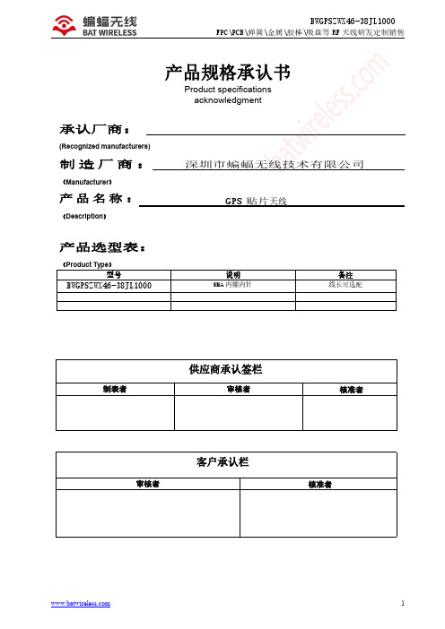
承认厂商:(Recognized制造厂商(Manufacturer)产品名称:GPS贴片天线(Description)产品选型表:(Product Type)型号说明备注BWGPSZWX46-38JL1000SMA内螺内针线长可选配供应商承认签栏制表者审核者核准者客户承认栏审核者核准者1.2AntennaPicture(可定制)*注:因天线功能较为敏感,主体周边机构有变更请通知我们评估。
上图型号:BWGPSZWX46-38JL10002.Electrical S pecification2.1Test EquipmentA.VSWR and input impedance:Agilent8753/E5071Network AnalyzerB.Antenna gain and efficiency:ETS three-dimensional anechoic chamber2.2Test Setup2.2.1Frequency Range2.2.2VSWRStep1:The antenna is arranged on the customer provided test fixture.Step2:The VSWR of the antenna is measured via Agilent8720/8753Network Analyzer(see figure.1).Figure.12.2.3Radiation pattern and GainA.The3D chamber provides less than-40dB reflectivity from800MHz to6GHz and a40cm diameterspherical quiet zone.The measurement results are calibrated using both dipoles and standard gainhorns(see figure.2).B.The antenna under tested is arranged in the turned table and a decoupling sleeve is used to reducefeed line radiation(see figure.3).C.The measured results of the radiation patterns and antenna gain are obtained from the controlsystem and showed on the monitor(see figure.4and5).Figure.2Figure.3Figure.4Figure.53.Performance Data3.1Passive dataVSWR(电压驻波比)/Return Loss(回波损耗)/Smith Chart(史密斯圆图)*注:以上为实测数据,仅供参考;因天线功能较为敏感,主体周边机构有变更请通知我们评估。
《微带贴片天线讲义》课件
提高微带贴片天线的效率可以提 高天线的辐射能力和能量利用率
。
04
PART 04
微带贴片天线的应用
无线通信系统
无线局域网(WLAN)
微带贴片天线广泛应用于无线局域网中,作为接入点(AP)和客户端(如笔记本 电脑和智能手机)的通信天线,实现高速数据传输。
蓝牙通信
蓝牙耳机和蓝牙设备中使用的微带贴片天线,用于无线传输语音和数据信号,方 便用户进行无线连接和通信。
雷达系统
车载雷达
在自动驾驶汽车中,微带贴片天线常 被用作车载雷达系统的发射和接收天 线,用于探测障碍物、车辆和行人的 位置和速度。
气象雷达
气象雷达中的微带贴片天线,能够发 射和接收微波信号,用于监测降雨、 风速、冰雹等气象信息。
卫星通信系统
卫星电视接收
微带贴片天线在卫星电视接收系统中应用广泛,用于接收来自卫星的电视信号,提供高清电视节目。
小型化和宽频带是微带贴片天线面 临的挑战之一,需要研究新型材料 和优化设计方法来实现。
高增益与低交叉极化问题
高增益
为了提高通信质量和距离,需要微带贴片天线具有较 高的增益。
低交叉极化
交叉极化会导致信号质量下降,因此需要微带贴片天 线具有较低的交叉极化。
总结
在提高增益的同时降低交叉极化是微带贴片天线的另 一个挑战,可以通过改进结构和材料来实现。
高效率与低成本问题
高效率
为了减少能量损失,微带贴片天线需要具有较高 的效率。
低成本
在满足性能要求的同时,降低微带贴片天线的制 造成本也是重要的考虑因素。
总结
高效率和低成本是微带贴片天线的第三个挑战, 可以通过优化制造工艺和采用新型材料来实现。
PART 06
一种新型微带贴片微波整流天线设计
一种新型微带贴片微波整流天线设计杨弋斓;刘长军【摘要】在微波无线能量传输系统中,整流天线广泛应用.为了解决整流天线中小型化的问题,对整流天线结构进行研究,提出一种新型整流天线设计.通过将天线和整流二极管阻抗直接共轭匹配进行设计,简化整流天线结构.该新型整流天线设计方法应用于2.45 GHz微带贴片微波整流天线中,用1 mm厚的F4B-2介质板设计和加工,设计出新型微带贴片整流天线,尺寸为70 mm×70 mm.实验结果显示,新型微带贴片整流天线最高整流效率为69.3%.新型整流天线相比传统整流天线具低剖面、轻重量、结构简化、低成本、容易加工和高射频-直流转换效率等优势,证明了该设计的有效性.%Rectennas are widely applied to wireless microwave power transmission systems.In order to realize the miniaturization of rectennas, the structures of rectennas were researched in this paper.This paper presented the design of a novel rectenna, in which the antenna impedance matches to the rectifying diode conjugation impedance directly.The impedances of antenna and rectifying diode were conjugate matched directly.The novel design method simplify the rectenna design.It is applied to a patch rectenna at 2.45 GHz.The novel patch rectenna was designed and fabricated on a 1 mm thick F4B-2 substrate with the physical dimension of 70 mm×70 mm.The highest measured MW-to-DC conversion efficiency at 2.45 GHz reached 69.3% in the experiment.The conclusion is that the novel rectenna has the advantages of low profile, light weight, structure simplification, low cost, and easy fabrication.Experiments prove the validity of the proposed design method.【期刊名称】《应用科技》【年(卷),期】2017(044)004【总页数】4页(P60-63)【关键词】微波;无线能量传输;整流天线;贴片天线;整流二极管;阻抗;共轭匹配;整流效率【作者】杨弋斓;刘长军【作者单位】四川大学电子信息学院,四川成都 610064;四川大学电子信息学院,四川成都 610064【正文语种】中文【中图分类】TN455微波无线能量传输(microwave wireless power transmission, MPT)是新能源领域的一个重要方向,吸引很多研究者的关注[1-4]。
用于WLAN的双频单极天线的设计
用于WLAN的双频单极天线的设计摘要无线局域网即WLAN是一架连接通信网与终端设备的桥梁。
随着该项技术的慢慢发展,WLAN在实际的生活以及工作中的应用愈渐普及。
无线局域网对天线有独特的要求是由其自身的特性决定的。
由此,应用于WLAN的天线需具备小型化、宽频带和双频段的特性以及要低剖面且易共形和易集成。
而微带天线的剖面低和易共形等优点几乎囊括了WLAN天线所要达到的这些特性要求,所以其对于无线局域网的实现来说是非常理想的选择。
本文章在对国内和国外相关文献研究的基础上,通过对微带线的学习、分析和仿真及针对WLAN标准的要求,在文中提出了一种用于无线局域网的双频印刷单极天线。
此款天线可以方便地植入到无线通讯设备中,并且有较强的实用性。
该天线是由50 的微带传输线通过耦合馈电的方式对其具有对称性结构的S型贴片馈电。
天线获得阻抗带宽可以覆盖无线局域网2.4GHz/5.2GHz/5.8GHz。
天线的总体尺寸为22mm×49mm,结构紧凑,便于加工,易于集成,适合于无线通讯中的应用。
文中给出了天线的设计及不同参数对天线性能的影响。
关键词:WLAN;S型贴片;单极天线;耦合馈电;双频;小型化AbstractWireless local area networks (WLAN) is a bridge connecting communication network and terminal equipment. With the gradual development of this technology, the application of WLAN in real life and work is becoming more and more popular. Wireless local area networks (WLAN) has unique requirements for antennas, which are determined by its own characteristics. Therefore, the antenna used in WLAN needs to have the characteristics of miniaturization, broadband and dual-band, as well as low profile, easy conformation and integration. However, the advantages of microstrip antenna such as low profile and easy conformal almost include these characteristics of WLAN antenna, so it is an ideal choice for the realization of WLAN.Based on the research of domestic and foreign literatures, this paper proposes a dual-band printed monopole antenna for WLAN by studying, analyzing and simulating microstrip lines and meeting the requirements of WLAN standard. The antenna can be easily implanted into the wireless communication equipment and has strong practicability. The antenna is composed of 50 microstrip transmission lines by means of coupling feed to the symmetry of the structure of the s-shaped tiles feeder. The impedance bandwidth acquired by the antenna can cover 2.4GHz/5.2GHz/5.8GHz of the wireless local area networks. The overall size of the antenna is 22mm×49mm. It has compact structure, easy to process and integrate. It is suitable for wireless communication applications. The design of the antenna and the influence of different parameters on the performance of the antenna are given.Key words: Wireless Local Area Networks; S-type patch; monopole antenna; coupling feed; double frequency;miniaturization目录第1章绪论 (1)1.1 研究背景及意义 (1)1.2 国内外研究现状 (1)1.3 论文主要内容 (3)第2章用于WLAN的双频印刷单极天线基本理论 (4)2.1 微带线馈电及耦合馈电 (4)2.2 微带天线的定义及分类 (4)2.3 单极天线基本参数及有限元数值分析法 (5)2.3.1 单极天线基本参数 (5)2.3.2 有限元数值分析法 (7)2.4 印刷单极天线工作原理 (7)2.5 天线的多频技术 (8)第3章WLAN、双频印刷单极天线的设计与分析 (9)3.1 天线的结构及分析 (9)3.2 天线的仿真设计与分析 (10)3.3 天线的各性能分析 (14)3.4 天线的总结 (16)第4章WLAN、双频印刷单极天线实物制作与分析 (17)4.1 天线的实物制作 (17)4.2 天线的分析 (17)4.3 天线小结 (19)第5章结束语 (20)参考文献 (20)致谢................................................................................................................................................................第1章绪论1.1 研究背景及意义无线局域网(WLAN)是一座把通信网络与终端设备连通的桥梁[1]。
宽频带正方形微带贴片天线的设计_王亚洲
2 i=1
hi
/
L
⎟⎟⎠⎞
−
1 2
(10)
∆L 是贴片的延伸量,由下式求得
∑ ∆L
=
0.412
2 i =1
hi
⎡ε
⎢ ⎣
ε
e
e + 0.3 − 0.258
⎤ ⎥ ⎦
•
⎢⎡⎜⎛
⎟⎞
∑ ⎢⎜
⎢⎜ ⎢⎜ ⎢⎣⎜⎝
L
2
hi
i=1
⎟ + 0.264⎟
⎟ ⎟⎠
⎜⎛
⎟⎞⎥⎤
∑ ⎜
⎜ ⎜ ⎜⎝
L
2
hi
i =1
+ 0.8⎟⎟⎥⎥ ⎟⎥ ⎟⎠⎥⎦
第 22 卷增刊
王亚洲等:宽频带正方形微带贴片天线的设计
31
图 4、图 5 分别是天线在 2.4GHz 和 3.1GHz 时 的远场辐射特性。通常情况下,宽频带天线在高频 时远场方向图容易出现裂瓣,本文设计的宽带天线 在工作频段内方向性基本良好。但是可以看出,随 着工作频率的提高,天线的方向性有变坏的趋势, 因此宽频带天线的高频辐射特性也是以后天线设 计过程中需要不断改进的方面。
42.3% (VSWR ≤ 2 ).
Key words:Broadband, Microstrip patch antenna, Impedance bandwidth
引言
本文介绍了一种新的宽频带微带贴片天线的设 计方法,给出了天线的测量和仿真结果。
微带天线由于具有剖面低、重量轻、成本低, 可与各种载体共形,适合印刷电路板技术批量生 产,便于实现圆极化、双极化、双频段工作等优点, 深受人们的关注,近年来应用也越来越广泛。但微 带天线有其固有缺陷,即阻抗带宽较窄,一般微带 天线的带宽仅有 5%左右[1,2]。微带天线的窄带特性 在很多方面限制了它的广泛应用,因此,展宽微带 天线的带宽具有十分重要的意义。
- 1、下载文档前请自行甄别文档内容的完整性,平台不提供额外的编辑、内容补充、找答案等附加服务。
- 2、"仅部分预览"的文档,不可在线预览部分如存在完整性等问题,可反馈申请退款(可完整预览的文档不适用该条件!)。
- 3、如文档侵犯您的权益,请联系客服反馈,我们会尽快为您处理(人工客服工作时间:9:00-18:30)。
I.J. Wireless and Microwave Technologies, 2016, 5, 35-44Published Online September 2016 in MECS()DOI: 10.5815/ijwmt.2016.05.04Available online at /ijwmtA Rectangular Microstrip Patch Antenna for WirelessCommunications Operates in Dual BandSheikh Dobir Hossain a, K. M. Abdus Sobahan b, Md. Khalid Hossain c*, Md. Masud AhamedAkash d, Rebeka Sultana e, Md. Masum Billah fa ,f Dept. of Physics, Jessore University of Science and Technology, Jessore-7408, Bangladeshb,d Dept. of Applied Physics, Electronics & Communication Engineering, Islamic University, Bangladeshc Institute of Electronics, Atomic Energy Research Establishment, Savar, Dhaka, Bangladeshe Department of Electrical and Electronic Engineering, Shizuoka University, Shizuoka, JapanAbstractA single layer substrate compact dual band rectangular micro-strip patch antenna with transmission line feeding is designed for Wireless Local Area Networks (WLAN) implementation. The desired antenna consists of a rectangular patch having two I-slots and a dielectric material with dielectric constant of 2.4. The use of cavity model with transmission line feed has the favor of low profile, high gain and wide bandwidth of the antenna. The antenna has overall size of 46.9 mm by 38.01 mm and gives bandwidth of about 90 MHz at resonance frequency of 2.45 GHz and that of 115 MHz at 4.1 GHz frequency with Defected Ground Structure (DGS). The antenna with DGS has return losses -21.25 dB at 2.45 GHz and -27.5 dB at 4.1 GHz where the gains are 6.70 dB for 2.45 GHz and 6.80 dB for 4.1 GHz. Finally the designed antenna has been simulated using Computer Simulation Technology (CST) microwave studio 2009 and it is comparable with manual computation results which are found to be suitable for WLAN applications.Index Terms: Micro-strip antenna; Cavity model; Dual band antenna; Coaxial probe feed.© 2016 Published by MECS Publisher. Selection and/or peer review under responsibility of the Research Association of Modern Education and Computer Science1. IntroductionThe wireless communication system has been developed rapidly in the past decades and it has already a dramatic impact on human life. In the last few years, the development of wireless local area networks (WLAN) represented one of the principal interests in the information and communication field. Thus, in commercial and government communication systems, it is required to develop low cost, minimal weight and low profile antennas that are capable of maintaining high performance over a large spectrum of frequencies. * Corresponding authorE-mail address: khalid.baec@This technological trend has focused on the design of micro-strip antennas with a simple geometry. Patch antennas offer many advantages that are not commonly exhibited in any other types of antenna configurations. Microstrip antennas are simple and inexpensive to fabricate using printed circuit board technology. They have extremely low profile and light weight [1]-[2]. They are compatible with microwave and millimeter-wave integrated circuits, and have the ability to conform to planar and non-planar surfaces. In addition, once the shape and operating mode of the patch are selected, designs become very versatile in terms of operating frequency, polarization pattern and impedance. The lower efficiency, higher value of Q, poor polarization purity, poor scan performance, spurious feed radiation and very narrow frequency bandwidth of a microstrip patch antenna have reduced their versatility. But in some applications where narrow bandwidth is desirable such as government security system the microstrip patch antenna are undeniable [3].However the larger bandwidth (as long as 90 percent) and good efficiency (up to about 35 percent) of the desired microstrip antenna can be achieved by increasing the thickness of the dielectric materials [4]. But when the height of the dielectric substance increases then there some power losses occur due to surface wave [5]-[6]. However there are some methods such as cavity method and stacking as well as other method are used to reduce the surface wave and hence the power losses while sustaining the large bandwidth and good efficiency [7]. Also both linear and circular polarization of a rectangular microstrip patch antenna has increased their versatility.2. Literature ReviewBefore the revolution (i.e. 1970) of electronic circuit miniaturization and large-scale integration in wireless communication the microstrip antenna (MSA) with conducting patch on a ground substrate was undeveloped. After that the radiations from radiating patch of a microstrip antenna with different configuration have been studied by many researchers. A low profile flush mounted microstrip antenna was the early work of Munson for the applications of rocket and missile practically. Gradually because of high demand in communication the multiband frequency modes operation can be obtained by using multilayer structures. To increase the fields of this antenna the various mathematical models were also developed. The last ten years papers or articles published in journals on these antennas show the importance gained by them. It is the most favorite choice to design micro strip antennas for the present day antenna designer’s[8]. The literature survey on microstrip antenna has discussed in this section.A couple line feed in a rectangular patch antenna is described by Van et al. [9]. The larger bandwidth antenna is obtained which is more than by a factor 2.5 than the normal edge fed patch antenna. Also the low physical dimension antenna is achieved over the previously available research while maintain their larger output. Chiba et al. introduced a dual-frequency planar antenna for handsets. The author has described an outer quarter-wavelength annular-ring with a short-circuited plane for a low resonance frequency and for high frequency response an inner quarter-wave length rectangular patch of a dual-band antenna [10]. Mark et al. proposed a L probe feed rectangular microstrip patch antenna for WLAN applications [11]. In this paper the author attains 36% impedance bandwidth and about 7-dBi average gain by introducing the attractive L shaped probe feed for the thick microstrip antenna. A U-slot rectangular patch on the substrate layer has been presented by Tong et al. [12]. Here due to the design of a broad-band -slot patch antenna on a microwave substrate the thickness of the desired antenna has increased than the case with a foam material. But the measured resonant frequencies and far-field patterns are well suited than the previous measured data and the gain of the desired antenna is about 6.5 dB. The authors have used a U-slot circular patch antenna with L-probe feeding and also there has been used foam substrate which is presented by Guo et al. in. Hence there obtained a larger bandwidth i.e. about 15% than that using the U-slot alone and about 14% than that using the L-probe alone [13].3. Experimental ModelThe geometry of the designed dual band rectangular micro-strip patch antenna using CST 2009 is shown in Fig.1. The designed dual band antenna operates at the resonant frequency of 2.76GHz and 5.9GHz. Due to the easy of fabrication and good impedance matching here we have used transmission line feeding technique. The thickness of substrate are taken between .003λo <h <.05 in order to achieve maximum bandwidth [14].Fig.1. Geometry of dual band MSAThe very popular and practical approximate for different parameter of rectangular microstrip patch antenna are [15]The width that’s leads to good radiation efficiencies is√ (1) Here,=Velocity of light=Resonant frequency=Dielectric constant of the substrateThe value of effective dielectric constant is(2)√Where, h is the thickness of the substrate and must be in mm unitThe normalized extension of the length is( )(3)( )The effective length of the patch is(4)Where actual length is(5)√4. Antenna Designed SpecificationThe different parameters of our designed dual band rectangular microstrip antenna are shown in table 1.Table 1. Various parameter of dual-band rectangular microstrip antennaParameters ValuesLength of the Patch (Lp) 38.01 mmWidth of the Patch (Wp) 46.9 mmDielectric constant of the Patch ( ɛr) 2.40Inset depth of the Patch (Y0) 13mmWidth of the Microstrip line (W f) 4.2mmWidth of the slots (W1) 1.4mmLength of the slots (L1) 14.2mmWidth of the non-radiating edges (S1) 1.4mmThickness of the Microstrip Patch (Mt) 0.1mmGap between transmission line and patch (Gpf) 1mm5. Simulation Results of Dual Band AntennaThe various parameters like Return loss, Voltage Standing Wave Ratio (VSWR) Smith chart, Directivity and Gain of this antenna are simulated using CST microwave studio 2009 as discussed in the following subsections.5.1 Return loss, VSWR and Smith chartThe return loss (RL) is the parameter which indicates the amount of power is lost in the load and does not return as a reflection. As already known, waves are reflected leading to the formation of standing waves when the transmitter and antenna impedance do not match. Hence the RL is the parameter similar to VSWR to indicate how well the matching between the transmitter and the antenna has taken place. Fig.2. Shows return loss of the designed rectangular Microstrip Antenna. Our designed antenna gives the return losses -21.25 dB and -27.5 dB at the resonance frequencies of 2.45 GHz and 4.1 GHz, respectively. As we know that the acceptable value of return loss is less than -10 dB, thus the results show that the designed antenna is perfectly matched and the power loss is minimum so the gain and efficiency is maximum [3]. And if we go through the below and upper ranges of these two resonance frequencies the antenna does not provides good impedance matching and hence the radiation from the antenna will be minimum. It also gives a bandwidth of approximately 90 MHz at 2.45 GHz and 115 MHz at 4.1 GHz which are applicable for Wireless Local Area Network.The voltage standing wave ratio (VSWR) is another parameter defined for antenna which determines that how well the antenna is matched. For a good antenna the value of VSWR is found less than or equal to 2 for practical antennas. Fig.3. and Fig.3. show the VSWR of the designed dual band rectangular microstrip patch antenna. From figures, it is clear that a VSWR of 1.3883 is found at the resonant frequency 2.45 GHz and thatof 1.0825 is found at the resonant frequency 4.1 GHz, which is below 2. Hence our designed antenna is perfectly matched with minimum loss.The smith chart of our designed antenna is shown in Fig.4. The figure shows that at resonant frequency 2.45 GHz the response locus lies above the real axis, hence it is inductive dominating and at resonant frequency 4.1 GHz the response locus lies below the real axis, hence it is capacitive dominating. The good impedance response is obtained by adding a series capacitor at the input with a reactance –j50 for 2.45 GHz frequecy and by adding a shunt capacitor at the input with a reactance –j50 for 4.1 GHz frequecy.From this chart it is clear that at both frequencies the impedance of the designed dual band antenna is 49 ohms which is approximately equal to the desired value of 50 ohms, indicating the minimum loss.Fig.2. Simulated return losses of dual band MSA at 2.45 GHz and 4.1 GHz(a)(b)Fig.3. The VSWR of dual band MSA at (a) 2.45 GHz; (b) 4.1 GHzFig.4.Smith Chart of dual band MSA at 2.45 GHz and 4.1 GHz5.2 Directivity and GainThe simulated results [3] of the directivity at 2.45 GHZ and 4.1 GHZ are shown in Fig.5. and Fig.6. respectively. The figure shows that it is a high directional antenna. From 2D and 3D pattern it is clear that the main lobe magnitudes are found 7.2 dBi in positive Z direction with angular width of 75.7 deg and 6.3dBi at an angle 49.0deg from positive Z direction with angular width of 68.5 deg at the resonant frequencies of 2.45 GHz and 4.1 GHz respectively which agree well with the previous results.The gains of the designed dual band antenna are given in Fig.7. and Fig.8. Since the graph represents that it is a high directional antenna so the gain of the antenna is high at a specific direction. The gains of the designed antenna are 6.698 dB and 6.797 dB at 2.45 GHz and 4.1 GHz frequencies, respectively. From 2D pattern it is also clear that the main lobe magnitudes are 6.7dB and 6.8dB and the directions of the main lobes are 0.0 deg. and 53 deg. with angular widths 75.7 deg. and 66.7 deg. at 2.45 GHz and 4.1 GHz frequencies, respectively which agrees well with the previous results.(a)(b)Fig.5.Directivity of dual band MSA at 2.45GHz (a) 2D pattern; (b) 3D pattern(a)(b) Fig.6.Directivity of dual band MSA at 4.1 GHz (a) 2D pattern; (b) 3D pattern(a)(b) Fig.7.Gain of dual band MSA at 2.45 GHz (a) 2D pattern; (b) 3D pattern(a)(b)Fig.8. Gain of dual band MSA at 4.1GHz (a) 2D pattern; (b) 3D pattern6. Summary of the ResultsThe results of the dual band rectangular microstrip antenna operating at 2.45 GHz and 4.1GHz are summarized in table 2.Table 2. Output parameters of the dual band MSA resonating at 2.45GHz and 4.1 GHz frequenciesResonating frequency fr (GHz) Return loss (dB) Bandwidth (MHz) VSWR Directivity (dB) Gain(dB)2.45 -21.25 90 1.3846 7.190 6.6984.1 -27.5 115 1.082 6.502 6.797The above table reflects that the designed antenna provides good impedance matching at two resonance frequencies of 2.45 GHz and 4.1 GHz with return losses of -21.25 dB and -27.5 dB respectively. So it is a dual band antenna with high directivities of 7.190 dB and 6.052 dB at these two resonance frequencies respectively. Due to the high directivity the gains of our designed antenna are higher.7. ConclusionsIn this paper, initially we have looked on the design and simulation of single band rectangular microstrip patch antenna and then extend it to dual band rectangular microstrip patch antenna. Here the various parameters like return loss, impedance, VSWR, directivity, gain, bandwidth and operating frequency are studied and also the effects of physical parametric on the performance of the designed antenna are studied. The designed dualband antenna shows good impedance matching of approximately 49 ohm’s. Also it provides good gain and efficiency at the resonant frequencies of 2.45 GHz and 4.41 GHZ which indicate that the designed antenna can be used for various applications like RADAR, Bluetooth, Biomedical instruments etc.AcknowledgementsWe would like to thank all concerned with the AECE department for their all-out effort to support us for completing this research.References[1]Shagun Maheshwari, Priyanka Jain, Archana Agarwal, “CPW-fed Wideband Antenna with U-shapedGround Plane,” I.J. Wireless and Microwave Technologies (IJWMT). Volume 5, November 2014.[2]Sheikh Dobir Hossain, K M Abdus Sobahan, Md. Khalid Hossain, Md. Khalid Hossain Jewel, RebekaSultana, Md. Al Amin, “A Linear Polarized Coaxial Feeding Dual Band Circular Microstrip Patch Antenna for WLAN Applications,” I.J. Wireless and Microwave Technologies (IJWMT). Vol. 1, 2016. [3] C.A. Balanis, Antenna Theory: Analysis and Design, Third Edition, ISBN 0-471-66782-X, Copyright2005 John Wiley & Sons, Inc.[4] D.M. Pozar, “Microstrip Antennas,” Proc. IEEE, Vol. 80, No. 1, pp. 79–81, January 1992.[5] C.M. Krowne, “Cylindrical-Rectangular Microstrip Antenna,” IEEE Trans. Antennas Propagat., Vol. AP-31, No. 1, pp. 194–199, January 1983.[6]I. Lier and K. R. Jakobsen, “Rectangular Microstrip Patch Antennas with Infinite and Finite Ground-PlaneDimensions,” IEEE Trans. Antennas Propagat., Vol. AP-31, No. 6, pp. 978–984, November 1983.[7]S.A. Long and M.D. Walton, “A Dual-Frequency Stacked Circular-Disc Antenna,” IEEE Trans. AntennasPropagat., Vol. AP-27, No. 2, pp. 270–273, March 1979.[8]Neha Parmar et al. “Review of Microstrip Patch Antenna for WLAN and WiMAX Application,” Int.Journal of Engineering Research and Applications ISSN: 2248-9622, Vol. 4, Issue 1(Version 1), January 2014, pp.168-171.[9]M.D. V an Wyk and K.D. Palmer, “Bandwidth enhancement of microstrip patc h antennas using coupledlines,” IEE Electronics Letters, Vol.37, No.13, pp.806-807, 2001.[10]N. Chiba, T. Amano and H. Iwasaki, “Dual-frequen cy planar antenna for handsets,”IEE ElectronicsLetters, Vol.34, No.25, 1998.[11]C.L. Mak, K.M. Luk, K.F. Lee, and Y.L. Chow, “Experimental Study of a Microstrip Patch Antenna withan L-Shaped Probe,” IEEE Transactions on antennas and propagation, Vo.48, No.5, May 2000.[12]Kin-Fai Tong, Kwai-Man Luk, Kai-Fong Lee, and Richard Q. Lee, “ A broadband U slot rectangularpatch anten na on a microwave substrate,” IEEE Transactions on antennas and propagation, Vol.48, No.6, pp. 954-961, 2000.[13]Y.X. Guo, K.M. Luk and K.F. Lee, “U-slot circular patch antennas with L-probe feeding,”IEEElectronics Letters, Vol.35, No.20, pp. 1694-1695, 1999.[14]Car ver, Keith R., and James Mink. “Microstrip antenna technology,”Antennas and Propagation, IEEETransactions , pp 2-24, Feb 1981.[15]C.A. Balanis, Advanced Engineering Electromagnetics, JohnWiley & Sons, New York, 1989.Authors’ ProfilesMr. Sheikh Dobir Hossain is working as a Lecturer in the dept. of Physics at Jessore Universityof Science and Technology, Jessore-7408, Bangladesh. He holds the degree of B.Sc & M.Sc inApplied Physics, Electronics & Communication Engineering from Islamic University, Kushtia-7003, Bangladesh. The fields of his research interest are wireless antenna design, wirelesscommunication, and material science.Mr. K. M. Abdus Sobahan received his PhD degree from the Inha University, South Korea. Hereceived h is Bachelor’s and Master’s degree from the dept. of Applied Physics &ElectronicsUniversity of Rajshahi, Rajshahi-6205, Bangladesh. Currently he is working as aprofessor in the dept. of Applied Physics, Electronics & Communication Engineering of IslamicUniversity, Kushtia-7003, Bangladesh.Mr. Md. Khalid Hossain has received the B.Sc (Hons) and M.Sc degree in Applied Physics,Electronics & Communication Engineering of Islamic University, Kushtia-7003. Currently he isworking as a Scientific Officer in the Institute of Electronics, AERE, Bangladesh Atomic EnergyCommission, Savar, Dhaka-1349, Bangladesh. His current interest are material science, nano-materials, dye-sensitized solar cell (DSSC), micro & nanofabrication, biosensor, RF MEMS,wireless antenna design. His work has produced 06 peer-reviewed scientific international journal papers.Mr. Md. Masud Ahamed Akash received his Bachelor’s and Master’s degree from the dept.of Applied Physics, Electronics & Communication Engineering of Islamic University, Kushtia-7003, Bangladesh. Now he is working as a System Engineer at Apple CommunicationLimited .His research interest includes Ad-hoc wireless communication, cellular mobilecommunication and optical fiber communication.Ms. Rebeka Sultana has been received B.Sc (Eng.) degree in Computer Science & Engineering(CSE) from University of Rajshahi, Rajshahi-6205, Bangladesh. Currently she is a MS studentof the Department of Electrical & Electronic Engineering (EEE), Shizuoka University, Japan.Her current research interest are computer vision, pattern recognition, image processing,artificial intelligence, signal processing, digital image processing, automatic control, wirelessantenna design and wireless communication.Mr. Md. Masum Billah received his B.Sc (Hons) and M.Sc degree in Physics from Universityof Dhaka, Bangladesh. Recently he is working as a Lecturer in the department of Physics atJessorec University of Science and Technology, Jessore-7408, Bangladesh. His research Interestfields are Biomedical Physics, Microelectronics, Laser Physics, High Energy Particle Physicsand mobile communication.。