合科泰常规厚膜片式电阻器规格书
厚膜贴片电阻

厚膜贴片电阻的原理、特点和应用厚膜贴片电阻是一种常见的被动元件,它是利用厚膜工艺将电阻性材料印刷在绝缘基体(如氧化铝陶瓷)上,然后经过高温烧结而成的。
厚膜贴片电阻具有体积小、功率大、耐热、耐冲击和耐腐蚀等优点,广泛应用于各种电子设备中,如智能手机、平板电脑、笔记本电脑、电视、汽车、医疗和军事设备等。
厚膜贴片电阻的原理厚膜贴片电阻的原理是利用电阻性材料的电阻率随温度的变化而变化的特性,通过控制印刷的厚度和图案,来调节电阻值。
电阻性材料一般是由金属粉末(如银、钯、铂等)和玻璃粉末混合而成的浆料,通过丝网印刷工艺将其印刷在绝缘基体上,形成一层或多层的厚膜。
厚膜的厚度一般在10微米到100微米之间,因此称为厚膜。
然后,将印刷好的基体放入高温炉中进行烧结,使浆料中的金属粉末和玻璃粉末熔化并固化,形成具有一定电阻率的均匀薄膜。
最后,通过激光切割或化学刻蚀等方法,在厚膜上切割出所需的图案,从而确定电阻值。
同时,在基体的两端印刷出导电性材料(如银或银钯合金),作为与外部电路连接的焊盘。
厚膜贴片电阻的特点厚膜贴片电阻具有以下几个主要特点:体积小、功率大。
由于厚膜贴片电阻是直接印刷在绝缘基体上,因此可以做到非常小的尺寸,如0075、01005、0201等。
同时,由于厚膜贴片电阻具有较高的耐热性和散热性,因此可以承受较大的功率,如0.125W、0.25W、0.5W等。
耐热、耐冲击和耐腐蚀。
由于厚膜贴片电阻采用了高温烧结工艺,因此具有较高的稳定性和可靠性,可以在-55℃到+155℃的温度范围内正常工作,并且不易受到机械冲击和化学腐蚀的影响。
适用于所有焊接工艺。
由于厚膜贴片电阻具有较高的耐热性和导电性,因此可以适应各种焊接工艺,如波峰焊、回流焊、手工焊等,并且在自动贴片应用中具有较高的稳定性和一致性。
成本低、产量高。
由于厚膜贴片电阻采用了丝网印刷工艺,因此可以实现批量生产,降低生产成本和时间。
同时,由于厚膜贴片电阻的材料和工艺相对简单,因此可以提供较多的规格和参数,满足不同的应用需求。
片式电阻尺寸表
片式电阻尺寸表一、尺寸定义片式电阻尺寸采用英制单位,主要包括长、宽和厚度三个维度。
长和宽的尺寸以英寸为单位,而厚度尺寸则以英寸的字母缩写表示。
例如,0201表示片式电阻的长和宽均为0.02英寸,而厚度的尺寸则由数字后面的字母来表示,如M表示0.125英寸,K表示0.156英寸等。
二、尺寸规格以下是一些常见的片式电阻尺寸规格:1.0201:长×宽×厚为0.02×0.02×0.125英寸。
2.0402:长×宽×厚为0.04×0.02×0.125英寸。
3.0603:长×宽×厚为0.06×0.03×0.156英寸。
4.0805:长×宽×厚为0.08×0.05×0.156英寸。
5.1206:长×宽×厚为0.12×0.06×0.2英寸。
这些规格中的数字代表了片式电阻的长和宽的尺寸,单位为英寸。
例如,0201表示片式电阻的长和宽均为0.02英寸,而厚度的尺寸则由数字后面的字母来表示,如M表示0.125英寸,K表示0.156英寸等。
三、尺寸与功率关系一般来说,片式电阻的尺寸越大,其所能承受的功率也就越大。
因此,在选择电阻时,需要根据实际应用场景选择合适的尺寸以满足功率需求。
四、尺寸与精度关系片式电阻的尺寸越大,其精度通常越高。
这是因为较大的电阻通常具有更均匀的阻值分布和更小的温度系数。
因此,在需要高精度的应用场景下,可以选择较大的片式电阻。
五、尺寸与温度系数关系片式电阻的尺寸也会影响其温度系数。
一般来说,较大的片式电阻具有更小的温度系数,即其阻值随温度的变化更小。
因此,在需要稳定性的应用场景下,可以选择较大的片式电阻。
综上所述,选择合适的片式电阻尺寸需要考虑实际应用场景中的功率、精度和稳定性等因素。
根据这些因素选择合适的片式电阻尺寸可以更好地满足实际需求。
固定厚膜贴片电阻器; 矩形型和高功率抗浪涌 RPCH16,20,32,35说明书

No.: RPCH-K-HTS-0001 /2Date: 2017.4.21Data sheetTitle: FIXED THICK FILM CHIP RESISTORS; RECTANGULAR TYPE AND HIGH POWER ⋅ ANTI SURGEStyle: RPCH16,20,32,35AEC-Q200 qualifiedRoHS COMPLIANCE ITEMHalogen and Antimony FreeNote: ・Stock conditionsTemperature: +5°C ∼+35°CRelative humidity: 25% ∼ 75%The period of guarantee: Within 2 year from shipmen t by the company.Solderability shall be satisfied.・Product specification contained in this data sheetare subject to change at any time without notice・If you have any questions or a Purchasing Specification for any quality Agreement is necessary, please contact our sales staff. ArrayHokkaido Research CenterApproval by: T. SannomiyaDrawing by: M. Shibuya1. Scope1.1 This data sheet covers the detail requirements for fixed thick film chip resistors; rectangular type & high power ⋅ anti surge,style of RPCH16,20,32,35.1.2 Applicable documentsJIS C 5201−1: 2011, JIS C 5201−8: 2014, JIS C 5201−8−1: 2014 IEC60115−1: 2008, IEC60115−8: 2009, IEC60115−8−1: 2014 EIAJ RC −2134C −20102. ClassificationType designation shall be the following form.(Example) RPCH 32 K 123 J TP 1 2 3 4 5 6 Style1 Fixed thick film chip resistors; rectangular type & & high power ⋅ anti surge2 Rated dissipation and / or dimension3 T emperature coefficient of resistance4 Rated resistance123 E24 Series, 3 digit, Ex. 123--> 12k Ω, 1000 E96 Series, 4 digit, Ex. 1000-->100Ω1022--> 10.2k Ω5 T olerance on rated resistanceD ±0.5% F ±1% J ±5%6 Packaging formB Bulk (loose package) TP Paper taping TE Embossed tapingK ±100×10−6/ °C−(Dash ) Standard Style3. Rating3.1 The ratings shall be in accordance with T able −1.T able −1StyleRated dissipation (W) T emperature coefficient of resistance (10-6 / °C) Rated resistance range (Ω)Preferred number series for resistors T olerance on rated resistance RPCH160.33K ±100 10∼1M E24, 96 D(±0.5%), F(±1%) Standard ±200 1.0∼9.76 K ±100 10∼1M E24 J(±5%) Standard ±200 1.0∼9.1 RPCH20 0.5K ±100 10∼1M E24, 96 D(±0.5%), F(±1%) Standard ±200 1.0∼9.76 K ±100 10∼1M E24 J(±5%) Standard ±200 1.0∼9.1 RPCH32 0.66K ±100 10∼1M E24, 96 D(±0.5%), F(±1%) Standard ±200 1.0∼9.76 K ±100 10∼1M E24 J(±5%) Standard ±200 1.0∼9.1 RPCH35 0.75K ±100 10∼1M E24, 96 D(±0.5%), F(±1%) Standard ±200 1.0∼9.76 K ±100 10∼1M E24J(±5%)Standard±200 1.0∼9.1Style Limiting element voltage(V) Isolation voltage(V) Category temperaturerange(°C)RPCH16 150150 −55~+155RPCH20200500RPCH32 RPCH353.2 Climatic category55/155/56 Lower category temperature − 55 °C Upper category temperature +155 °C Duration of the damp heat, steady state test 56days 3.3 Stability class5% Limits for change of resistance:−for long −term tests ±(5%+0.1Ω) −for short −term tests ±(1%+0.05Ω)3.4 DeratingFigure–1 Derating curveAmbient temperature (°C)3.5 Rated voltaged.c.or a.c.r.m.s.voltage calculated from the square root of the product of the rated resistance and the rated dissipation. E: Rated voltage (V)E =P ·RP: Rated dissipation (W) R: Rated resistance (Ω)Limiting element voltage can only be applied to resistors when the resistance value is equal to or higher than the criticalresistance value.At high value of resistance, the rated voltage may not be applicable.4. Packaging formThe standard packaging form shall be in accordance with T able −2.T able −2Symbol Packaging form Standard packagingquantity / unitsApplicationB Bulk (loose package) 1,000 pcs .RPCH16,20,32,35 TP Paper taping 8mm width, 4mm pitches 5,000 pcs. RPCH16,20,32TE Embossed taping8mm width, 4mm pitches 4,000 pcs. RPCH355. Dimensions5.1 The resistor shall be of the design and physical dimensions in accordance with Figure −2 and T able −3.Figure −2T able −3 Unit: mmStyle L W H c d RPCH16 1.6±0.1 +0.15 0.8 -0.05 0.45±0.10 0.3±0.2 0.3±0.1 RPCH20 2.0±0.1 1.25±0.10 0.55±0.10 0.3±0.2 0.4±0.2 RPCH32 3.1±0.1 1.6±0.15 0.55±0.10 0.4±0.25 0.5±0.25 RPCH35 3.1±0.15 2.5±0.15 0.55±0.15 0.4±0.25 0.5±0.255.2 Net weight (Reference)Style Net weight(mg) RPCH16 2 RPCH20 5 RPCH32 9 RPCH35 166. MarkingResistorThe Rated resistance shall be marked in 3 digits (E24) or 4 digits (E96) and marked on over coat side.• E24 series: 3 digits, E96 series: 4 digitsIn case of the resistance value that E96 overlaps with E24, It is marked by either.The Rated resistance of RPCH16 should not be marked in 4 digits(E96)Marking example Contents Application123 12×10 3 [Ω]→ 12 [kΩ]E24(RPCH16,20,32,35)2R2 2. 2[Ω]E24(RPCH 16,20,32,35)5623 562 ×103 [Ω] → 562 [kΩ] E96(RPCH 20,32,35)12R7 12.7 [Ω] E96(RPCH 20,32,35)7. Performance7.1 The standard condition for tests shall be in accordance with Sub−clause 4.2, JIS C 5201−1: 2011.7.2 The performance shall be satisfied in T able−4.T able−4(1)No. T est items Condition of test (JIS C 5201−1) Performance requirements1 Visual examination Sub−clause 4.4.1Checked by visual examination. As in 4.4.1The marking shall be legible, as checked by visual examination.2 DimensionResistance Sub−clause 4.4.2Sub−clause 4.5As specified in T able−3 of thisspecification.As in 4.5.2The resistance value shallcorrespond with the rated resistancetaking into account the specifiedtolerance.3 Voltage proof Sub−clause 4.7Method: 4.6.1.4T est voltage: Alternating voltage with a peakvalue of 1.42 times the insulationvoltage.Duration: 60 s ± 5 sInsulation resistanceT est voltage: Insulation voltageDuration: 1 min. No breakdown or flash over R ≥ 1 G Ω4 Solderability Sub−clause 4.17Without ageingFlux: The resistors shall be immersed in anon−activated soldering flux for 2s.Bath temperature: 235 °C ± 5 °CImmersion time: 2 s ± 0.5 s As in 4.17.4.5The terminations shall be covered with a smooth and bright solder coating.T able −4(2)No T est items Condition of test (JIS C 5201−1)Performance requirements 5Mounting Overload (in the mounted state) Solvent resistance of the marking Sub −clause 4.31 Substrate material: Epoxide woven glass Sub −clause 4.13 The applied voltage shall be 2.5 times the rated voltage or twice the limiting element voltage, whichever is the less severe. Duration: 2 s Visual examination ResistanceSub −clause 4.30 Solvent: 2−propanolSolvent temperature: 23 °C ± 5 °C Method 1Rubbing material: cotton wool Without recoveryNo visible damage ∆R ≤ ± (1%+0.05Ω) Legible marking6Mounting Bound strength of the end face plating Final measurements Sub −clause 4.31 Substrate material: Epoxide woven glass Sub −clause 4.33 Bent value: 3 mm Resistance Sub −clause 4.33.6 Visual examination∆R ≤ ± (1%+0.05Ω) No visible damage7Resistance to soldering heat Component solvent resistance Sub −clause 4.18 Solder temperature: 260 °C ± 5 °C Immersion time: 10 s ± 0.5 s Visual examination Resistance Sub −clause 4.29 Solvent: 2−propanolSolvent temperature: 23 °C ± 5 °C Method 2Recovery: 48 h Visual examination ResistanceAs in 4.18.3.4No sign of damage such as cracks. ∆R ≤ ± (1%+0.05Ω)No visible damage ∆R ≤ ± (1%+0.05Ω)T able −4(3)No T est itemsCondition of test (JIS C 5201−1)Performance requirements 8MountingAdhesionRapid change temperatureSub −clause 4.31Substrate material: Epoxide woven glass Sub −clause 4.32 Force: 5 NDuration: 10 s ± 1 s Visual examination Sub −clause 4.19Lower category temperature:−55 °C Upper category temperature:+155 °CDuration of exposure at each temperature: 30 min.Number of cycles: 5 cycles. Visual examination ResistanceNo visible damageNo visible damage ∆R ≤ ±(1%+0.05Ω) 9Climatic sequence −Dry heat−Damp heat, cycle (12+12hour cycle) First cycle−Cold−Damp heat, cycle (12+12hour cycle) Remaining cycle−D.C. loadSub −clause 4.23 Sub −clause 4.23.2T est temperature: +155 °C Duration: 16 h Sub −clause 4.23.3 T est method: 2T est temperature: 55 °C [Severity(2)]Sub −clause 4.23.4T est temperature −55 °C Duration: 2hSub −clause 4.23.6 T est method: 2T est temperature: 55 °C [Severity (2)]Number of cycles: 5 cycles Sub −clause 4.23.7The applied voltage shall be the rated voltage or the limiting element voltage whichever is the smaller.Duration: 1 min. Visual examination ResistanceNo visible damage ∆R ≤ ± (5%+0.1Ω) 10MountingEndurance at 70 °C Sub −clause 4.31Substrate material: Epoxide woven glass Sub −clause 4.25.1Ambient temperature: 70 °C ± 2 °C Duration: 1000 hThe voltage shall be applied in cycles of 1.5 h on and 0.5 h.The applied voltage shall be the rated voltage or the limiting element voltage whichever is the smaller.Examination at 48 h , 500 h and 1000 h:Visual examination ResistanceNo visible damage ∆R ≤ ± (5%+0.1Ω)T able −4(4)No T est items Condition of test (JIS C 5201−1)Performance requirements 11Mounting V ariation of resistance with temperature Sub −clause 4.31 Substrate material: Epoxide woven glass Sub −clause 4.8 −55 °C / +20 °C+20 °C / +155°CAs in T able −112Mounting Damp heat, steady state Sub −clause 4.31 Substrate material: Epoxide woven glass Sub −clause 4.24Ambient temperature: 40 °C ± 2 °C +2 Relative humidity : 93 % −3 a) 1st group: without voltage applied.b) 2nd group: The d. c. voltage shall be appliedcontinuously .The voltage shall be accordance with Sub −clause 4.24.2.1 b). without polarizing voltage [4.24.2.1, c)] Visual examinationResistanceNo visible damage Legible marking ∆R ≤ ± (5%+0.1Ω) 13Dimensions (detail) Mounting Endurance at upper category temperature Sub −clause 4.4.3 Sub −clause 4.31 Substrate material: Epoxide woven glass Sub −clause 4.25.3 Ambient temperature:155 °C ± 2 °CDuration: 1000 hExamination at 48 h, 500 h and 1000 h:Visual examination Resistance As in T able −3No visible damage ∆R ≤ ± (5%+0.1Ω)8. T aping8.1 Applicable documents JIS C 0806−3: 2014, EIAJ ET −7200C: 2010 8.2 T aping dimensions8.2.1 T aping dimensions shall be in accordance with Figure −3 and T able −5.Unit: mmFigure −3T able −5 Unit: mmStyle A B t 1 t 2 RPCH16 1.15±0.15 1.9±0.2 0.6±0.1 0.8max. RPCH20 1.65±0.15 2.5±0.2 0.8±0.1 1.0max. RPCH32 2.00±0.15 3.6±0.2 0.8±0.1 1.0max.8.2.2 Embossed taping dimensions shall be in accordance with Figure −4 and T able −6.Unit: mmFigure −4T able −6 Unit: mmStyle A B W E t 1 RPCH35 2.85±0.20 3.5±0.2 8.0±0.3 3.5±0.05 1.0±0.21). The cover tapes shall not cover the sprocket holes.2). T apes in adjacent layers shall not stick together in the packing. 3). Components shall not stick to the carrier tape or to the cover tape. 4). Pitch tolerance over any 10 pitches ±0.2mm.5). The peel strength of the top cover tape shall be with in 0.1N to 0.5N on the test method as shown in the followingRPCH16,20,32:Figure −4,RPCH35:Figure-5.6). When the tape is bent with the minimum radius for 25 mm, the tape shall not be damaged and the components shallmaintain their position and orientation in the tape.7). In no case shall there be two or more consecutive components missing.The maximum number of missing components shall be one or 0.1%, whichever is greater. 8). The resistors shall be faced to upward at the over coating side in the carrier cavity .Figure −5Figure −6/min )165°to180°Carrier tape T op cover tapeP eel −off(About 300mm /min )Direction of unreelingNo: RPCH −K −HTS −0001 /2Title:FIXED THICK FILM CHIP RESISTORS; RECTANGULAR TYPE ANDHIGH POWER ⋅ ANTI SURGE RPCH16,20,32,35Page: 10/10Product specification contained in this data sheet are subject to change at any time without notice.If you have any questions or a Purchasing Specification for any quality agreement is necessary, please contact our sales staff.Issue: KAMAYA ELECTRIC CO., LTD. Research & Development Department HOKKAIDO Research center Last update: 2017.4.218.3 Reel dimensionReel dimensions shall be in accordance with the following Figure −7 and T able −7.T able −7 Unit: mmStyleA B Note RPCH16,20,32,35 +1.0 9 011.4±1.0 Injection molding13±1.0 V acuum formingNote : Marking label shall be marked on a place of Marking A or two place of marking A and B.Figure −89. Marking on packageThe label of a minimum package shall be legibly marked with follows. 9.1 Marking A(1) Classification(Style, T emperature coefficient of resistance, Rated resistance, T olerance on rated resistance, Packaging form)(2) Quantity (3) Lot number (4) Manufacturer’s name or trade mark (5) Others9.2 Marking B (KAMA Y A control label)。
片式厚膜电阻器

片式厚膜电阻器片式厚膜电阻器,是一种常见的电阻器类型,具有许多优点和广泛的应用。
本文将从厚膜电阻器的原理、结构、特点和应用等方面进行介绍。
一、厚膜电阻器的原理厚膜电阻器是利用厚膜工艺在陶瓷或玻璃基片上制作电阻材料,再通过蒸镀、丝印等工艺形成导线和引线,最后在高温烧结过程中形成电阻器结构。
厚膜电阻器的电阻值由电阻材料的阻值、长度和宽度决定。
二、厚膜电阻器的结构厚膜电阻器一般由基片、电阻材料、电极、引线和封装等部分组成。
基片作为电阻器的基础,一般采用陶瓷或玻璃材料;电阻材料是通过厚膜工艺在基片上制作的,常见的材料有铬、铜、镍等;电极是连接电阻材料的导线,常见的形式有蒸镀、丝印等;引线是将电阻器连接到电路中的导线,一般采用金属材料;封装是将电阻器保护起来,常见的封装有贴片式、插件式等。
三、厚膜电阻器的特点1. 高精度:厚膜电阻器的电阻值精度高,一般可达到1%或更高。
2. 耐高温:厚膜电阻器可以在高温环境下工作,一般可耐受几百摄氏度的温度。
3. 耐腐蚀:厚膜电阻器的电阻材料往往具有良好的耐腐蚀性能,可以在恶劣的环境下使用。
4. 体积小:厚膜电阻器的体积相对较小,适合在空间有限的电路中使用。
5. 成本低:相比于其他类型的电阻器,厚膜电阻器的制造成本相对较低。
四、厚膜电阻器的应用厚膜电阻器广泛应用于各种电子设备和电路中,主要包括以下几个方面:1. 电源供应:厚膜电阻器常用于电源供应电路中的电流限制、电压分压等功能。
2. 信号处理:厚膜电阻器用于信号处理电路中的电流测量、电阻匹配等。
3. 温度测量:厚膜电阻器可以作为温度传感器使用,常用于温度测量和控制中。
4. 自动控制:厚膜电阻器常用于自动控制电路中的反馈、调节和保护等功能。
5. 通信设备:厚膜电阻器用于通信设备中的阻抗匹配、滤波等。
片式厚膜电阻器是一种常见的电阻器类型,具有高精度、耐高温、耐腐蚀、体积小和成本低等特点。
它广泛应用于电子设备和电路中的电源供应、信号处理、温度测量、自动控制和通信设备等领域。
片式电阻尺寸表

片式电阻尺寸表
一般情况下,片式电阻的尺寸表包括以下几个参数:
1. 长度(Length):片式电阻的整体长度,通常以毫米(mm)为单位。
2. 宽度(Width):片式电阻的整体宽度,通常以毫米(mm)为单位。
3. 厚度(Thickness):片式电阻的整体厚度,通常以毫米(mm)为单位。
4. 电阻面积(Resistance Area):片式电阻器的电阻发热区域
的面积,通常以平方毫米(mm²)为单位。
5. 电阻值(Resistance Value):片式电阻器的电阻值,通常以欧姆(Ω)为单位。
6. 容差(Tolerance):片式电阻器的电阻值允许的偏差范围,通常以百分比形式表示。
7. 最大功率(Maximum Power):片式电阻器能够承受的最大功率,通常以瓦特(W)为单位。
需要注意的是,片式电阻的尺寸表可能会因不同的制造商、型号和尺寸而有所差异,上述参数仅为常见参数,具体以实际产品规格为准。
厚膜片式跨接电阻器

Standard
负荷下降曲线 Derating Curve
-55
70
100
75
50
25
使用温度范围
Operating Temperature Range
-55 125
额定负荷百分比 Percent rated load
-75 -50 -25
0
25 50 75 100 125 155
环境温度 Ambient temperature ( )
型号 Type 0201 0402 0603 0805 1206 1210
P 2.0 0.05 2.0 0.05 4.0 0.1 4.0 0.1 4.0 0.1 4.0 0.1
P0 4.0 0.1 4.0 0.1 4.0 0.1 4.0 0.1 4.0 0.1 4.0 0.1
P1 2.0 0.05 2.0 0.05 2.0 0.05 2.0 0.05 2.0 0.05 2.0 0.05
广东风华高新科技股份有限公司
Fenghua Advanced Technology (holding) Co., Ltd
产品外观 Appearance
1.电阻器表面二次玻璃体保护膜覆盖完好且难以脱落,表面平整 The surface of resistor is covered with Protective Coating which hard to fade, and the surface of coating should avoid unevenness.
贴片电阻的识别

常见电阻的识别KOA(兴亚)电阻识别:RK73B2A T TD1001J(1)(2)(3)(4)(5)(6)(1)产品类型:(2)额定功率:代码功率1E1/8W1J1/5W2A1/4W2B1/2W2H3/4W3A1W (3)端电极处理形式:代码端电极处理形式T Sn(4)编带方式:(5)标称电阻值:代码电阻值空白0Ohm10011K Ohm1021K Ohm4700470Ohm470R470Ohm60.4R60.4Ohm60R460.4Ohm220222.0K Ohm22322.0K Ohm (6)电阻精度:代码精度D±0.5%F±1%G±2%J±5%K±10%ROHM(罗姆)电阻识别:MCR01MZP J102(1)(2)(3)(4)(5)(1)电阻类型:代码类型MCR厚膜电阻器PMR金属盘电阻器ESR抗波动型厚膜电阻器KTR耐高压厚膜电阻器MNR网络型厚膜电阻器RCN贴片式衰减型厚膜电阻器MVR贴片式微条型厚膜电阻器(2)封装尺寸、功率及耐压:代码型号英制长×宽功率耐压00602010.6×0.3mm1/20W25V 010402 1.0×0.5mm1/16W50V 030603 1.6×0.8mm1/10W50V 100805 2.0×1.25mm1/8W150V (3)元件个数:代码个数JZH4000EZH5000HZP2000EZP5000MZP10000YZP15000EOAP5000MOAP10000HXBR2000IXBR3000KXBR5000(4)电阻精度:代码精度D±0.5%F±1%G±2%J±5%K±10%(5)标称电阻值:代码电阻值0000Ohm1021K Ohm UNIOHM(厚声)电阻识别:1206S4J012J T5E(1)(2)(3)(4)(5)(6)(7)(1)封装尺寸:型号公制型号英制长×宽050302010.5×0.25mm10050402 1.0×0.5mm16080603 1.5×0.76mm20120805 2.0×1.25mm32161206 3.2×1.6mm32251210 3.2×2.5mm45321812 4.5×3.2mm (2)额定功率:代码功率WM1/20WWG1/16WWA1/10WW81/8WW41/4WW21/2W073/4W1W1W1A1/10WSS81/8WSS41/4W-SU21/2WSSS21/2W-S073/4W-S(3)电阻精度:代码精度D±0.5%F±1%G±2%J±5%(4)标称电阻值:代码电阻值100210K Ohm10011K Ohm00000Ohm012J 1.2Ohm012K0.12Ohm012L0.012Ohm注:前三位表示有效数字,后一位表示有几个0,其中J=0.1,K=0.01,L=0.001。
薄膜贴片电阻器规格书_风华_FH
1/4W 150 300
1/2W 150 300
Special Ratings
Item
0402
0603
0805
1206
1210
2010
2512
Power Rating
1/16W
1/16W
1/10W
1/8W
1/4W
1/4W
1/2W
Max.Working
25
Voltage(V)
50
100
150
150
150
within specified T.C.R
MIL-STD-202F Method 304 +25/-55/+25/+125/+25
R
0.05%R+0.05
JIS-C-5202-7.2
R
0.5%R+0.05
2.5
5 :For thin film chip resistor with high power series: RCWV2.5 or Max Overload Voltage,
0.01% 0.05% 0.10%
0.10% 0.25% 0.50%
Operating Temperature Range
-55 ~+155
Characteristics
Item
Specifications
(GB/T 5729-2003) Test Method(GB/T 5729-2003)
T.C.R
unit:mm
a
b
0.20 0.10 0.30 0.20 0.30 0.20 0.40 0.20 0.50 0.20 0.60 0.20 0.60 0.20
- 1、下载文档前请自行甄别文档内容的完整性,平台不提供额外的编辑、内容补充、找答案等附加服务。
- 2、"仅部分预览"的文档,不可在线预览部分如存在完整性等问题,可反馈申请退款(可完整预览的文档不适用该条件!)。
- 3、如文档侵犯您的权益,请联系客服反馈,我们会尽快为您处理(人工客服工作时间:9:00-18:30)。
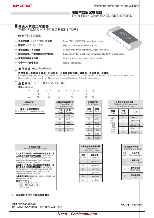
1.品名的构成
例如:RI0603L1003FT
RI
0603
L
1003
F
T
产品代号: RI 表示厚 膜片式固 定电阻
规格型号: 0201 0402 0603 0805 1206 1210 1812 2010 2512
2.结构
温度系数:L 1%=100PPM 5%=200PPM
1Ω~10Ω 10Ω~22MΩ ----------
1Ω~10Ω 10Ω~22MΩ ----------
0ohm Jumper
0ohm Jumper 最大电
流
50mΩ MAX
0.5A
50mΩ
1A
MAX
50mΩ
1A
MAX
50mΩ MAX
1.5A
50mΩ MAX
1.9A
50mΩ MAX
2.2A
50mΩ
3A
1Ω~10Ω 10Ω~10MΩ ----------
1Ω~10Ω 10Ω~10MΩ ----------
1Ω~10Ω 10Ω~10MΩ ----------
1Ω~10Ω 10Ω~10MΩ ----------
1Ω~10Ω 10Ω~10MΩ ----------
J(±5%) E24
1Ω~25Ω
25Ω~10MΩ
1Ω~10Ω ---------10Ω~10MΩ
1Ω~10Ω ---------10Ω~10MΩ
1Ω~10Ω ---------10Ω~10MΩ
1Ω~25Ω
25Ω~10MΩ
1Ω~10Ω 10Ω~10MΩ ----------
1Ω~10Ω 10Ω~10MΩ ----------
1Ω~10Ω 10Ω~10MΩ ----------
T 0.23±0.03 0.35±0.05 0.45±0.10 0.50±0.10 0.55±0.10 0.55±0.15 0.55±0.15 0.55±0.15 0.55±0.15
E 0.15±0.05 0.15±0.10 0.25±0.20 0.35±0.20 0.45±0.25 0.50±0.25 0.50±0.25 0.65±0.25 0.85±0.25
e 0.15±0.05 0.20±0.10 0.30±0.20 0.40±0.20 0.40±0.25 0.50±0.35 0.50±0.35 0.50±0.25 0.95±0.25
功率 型别
最大
70℃ 工作
电压
0201 1/20W 25V
最大过 负荷电
压
50V
T.C.R (ppm/℃)
±600 ±250
电阻值: 三 位 数 (E24 系 列)前面两位表 示有效数字。第 三位表示有效数 字后零的个数。 四位数(E96 系 列)前三位表示 有效数字,第四 位表示有效数字 后零的个数。 例如: 103=10K 欧 1003=100K 欧 1R0=1 欧
阻值误差: B=±0.1% D=±0.5% F=±1% J=±5%
±200 ±100
-------------------
1812 3/4W 2010 3/4W 2512 1W
200V 200V 200V
400V 400V 400V
+500~-250 ±200 ±100
+500~-250 ±200 ±100
+500~-250 ±200 ±100
----------------------------------------------------------------------------------
规格 0201 0402 0603 0805 1206 1210 1812 2010 2512
L 0.60±0.03 1.00±0.05 1.60±0.15 2.00±0.15 3.10±0.15 3.10±0.15 4.50±0.15 5.00±0.20 6.25±0.20
W 0.30±0.03 0.50±0.05 0.80±0.10 1.25±0.15 1.60±0.15 2.50±0.15 3.20±0.15 2.50±0.20 3.10±0.20
MAX
50mΩ
3A
MAX
50mΩ 3A
MAX
GUANGDONG HOTTECH INDUSTRIAL CO., LTD
Page:P11-P2
合科泰常规厚膜片式电阻器规格书
4.字码
4.1 (大于 1Ω表示方法) *0201、0402 因电阻本体太小,固无印记表示。 *公差为±0.1%、±0.5%、±1%的用四位数表示,前三位表示有效数字,第四位表示乘幂(10V)。
阻值范围
F(±1%) E96
G(±2%) E24
1Ω~25Ω
25Ω~10MΩ
1Ω~10Байду номын сангаас ---------10Ω~10MΩ
1Ω~10Ω ---------10Ω~10MΩ
1Ω~10Ω ---------10Ω~10MΩ
1Ω~10Ω ---------10Ω~10MΩ
1Ω~10Ω ---------10Ω~10MΩ
0805 1/8W 1206 1/4W
150V 300V 200V 400V
+500~-250 ----------
±200 ±100
---------10Ω~1MΩ
+500~-250 ----------
±200 ±100
---------10Ω~1MΩ
1210 1/2W
200V 400V
+500~-250 ----------
D(±0.5%) E96
-------------------
0402 1/16W 50 V 0603 1/10W 50V
100V 100V
+500~-250 ----------
±200 ±100
-------------------
+500~-250 ----------
±200 ±100
---------10Ω~1MΩ
包装方式: T: 编 带 包 装
2
31 4 5 6
7 8 9
1.外保护层 7.镀镍层
2.字码印记 3.内保护层 4.阻体层
8.镀锡层
9. 陶瓷基体
5.导体层
6.侧面导体层
GUANGDONG HOTTECH INDUSTRIAL CO., LTD
Page:P11-P1
合科泰常规厚膜片式电阻器规格书
3.尺寸和电性参数
1Ω~10Ω 10Ω~22MΩ ----------
1Ω~10Ω 10Ω~22MΩ ----------
1Ω~10Ω 10Ω~22MΩ ----------
1Ω~10Ω 10Ω~22MΩ ----------
1Ω~10Ω 10Ω~22MΩ ----------
1Ω~10Ω 10Ω~22MΩ ----------