lm298应用资料
夏米尔慢走丝290-500操作说明书
夏米尔慢走丝操作说明书1.目的为正确操作线切割设备以维持线切割设备之精度及稳定性,延长其使用寿命,使线切割加工作业规范.标准化,而达到提升质量保证,提升加工效率的目的,以满足客户需求.2.适用范围适合于ROBOFIL290.ROBOFIL500型号之慢走丝.3.作业内容3.1 开机当电柜合闸通电的时候,数控恢复断电前的状态.如果想装软件,必须启动特别的启动屏幕,步骤如下:3.1.1 按通电开关.3.1.2 同时,按住控制板上任何一个键,直到显示启动屏幕.3.1.2.1 监控功能(MONITOR)是保留给CT维修服务人员的.3.1.2.2 装入功能(LOAD)用来装软件模块:系统.自诊断.3.1.2.3 初始化功能(INITALIZE)数控返回到初始状态(相当于装入软件的状态).3.1.2.4 继续功能(CONTINUE)用于退出特别启动屏幕,进入正常操作(象上面的操作一样,激活最后一个屏幕).3.2 安装软件3.2.1 系统软件一旦初始化菜单被激活,接着:* 把系统盘(磁盘A)插入驱动器A* 选择LOAD(F2)在装软件期间,磁盘驱动器二极管和屏幕右一指灯亮,数控显示装入过程的信息.装入结束后,NC在EXE方式下,以便执行装入下列文件的操作.(语言,CT-EXPERT.CAM-CT)3.2.2. 装入系统软件后,显示语言配置菜单:* 指明所需要的语言名,用RETURN确认* 根据指示插入所选择的语言盘* 按F1(寻找)输入必须的文件,设备即按所选语言配置.3.3 屏幕组织* 准备模式(PREPARATION) 符号: PREP 背景色: 绿色* 执行模式(EXECTION) 符号: EXE 背景色: 紫色* 信息模式(INFORMATION) 符号: INFO 背景色: 蓝色* 图形模式(GRAPIC) 符号: GRAPH 背景色: 橙色3.3.1 PREP 准备方式3.3.1.1 编辑器(EDITOR)该功能用来建立或修改ISO程序,控制程序PROFIL程序1): 寻找文本(FIND.TEXT)2): 寻找下一个(FIND NEXT)3): 块(BLOCK)4): 标记范围开始(MARK START>标记范围结束(MARK END)5): 保存文件(SAVE FILE)6): 退出(EXIT)3.3.1.2 CAM-CT* 准备ISO零件程序需要交替运用菜单功能与绘图功能.<此单节介绍略>3.3.1.3 专家系统(CT-EXPERT)* 这些程序可以手工或者由CT-EXPERT专家系统自动生成.* 与不使用CT-EXPERT专家系统相比,CT-EXPERT生成的TEC文件是分完整的.用一个TEC文件,一个ISO文件和一个命令文件就可能执行个加工操作.相反,当一个文件在CT-EXPERT中查询或者修改时,必须3.3.1.4 文件(FILES)* 本功能用于处理存储在(所用的)不同单元上的所有文件(选择一个单示其下的文件目录).* 可以对给定目录中的文件操作,或者从一个目录转到另一个目录.1): 拷贝(COPY)2): 删除(DELETE)3): 改变名称(RENAME)4): 显示(DESPLAY)5): 打印(PRINT)6): 转换单元(CHANGE UNIT)7): 格式化(INITIALISE)8): 退出(EXIT)3.3.1.5 表编辑(EDIT TABLES)1): TEC--规准表(工艺文件的定义)2): OFS--偏移量(补正量)3): VAR--变量(变量值代入)4): WIR--电极丝(使用线参数)3.3.2. EXECUTION执行方式* 配置机台* 调节多种参数* 运行测量功能* 在开始加式操作之前,执行所需要的测试3.3.2.1. 执行程序(PROGRAM EXECUTION)1). 切割(CUT)2). 空跑(DRY RUN)3). 检验(VERIFY)4). 绘图(DRAW ON SCREEN)5). 改变模式(CHANGE UNIT)3.3.2.2. 用户参数(USER PARAMETERS)1) HPA: 工件设度2) CLE: 补偿间隙3) SCF: 比例系数4) ROT: 工件旋转5) TFE: 补正量认可6) TRE: 斜度认可7) MIR,X: X镜像8) MIR,Y: Y镜像9) ZID: 下导头至平台距离10) ZSD: 上导头至工件顶部距离11) BLK: 单节执行12) CBC: 一个命令一个命令执行13) SIM: 加工与空跑转换14) TSIM: 模拟穿丝15) VSIM: 空跑速度16) BLD: 遇"/"跳过17) OSP: 选择性暂停18) ENG: 选择单位19) COE: 遇不错误继续执行20) ART: 断电后自动重启动21) ATH: 断丝后重穿丝22) CHRA: 选择表面精度的单位23) WIRE LN : 电极丝的消耗量24) MIOL: 测量允许的误差25) DVI: 缺省使用的源外设26) EXT: 缺省扩展27) DEIO: 电介液的导电率28) ATT: 开始切入路径的长度29) EAO: 遥控报警3.3.2.3: 电源参数(GENERAO PARAMETERS)* EL: 使用的电极丝号* PA: 工件的材料号1) FF: 暂时降低频率2) M : 切割方式3) V : 切割电压4) A : 脉冲宽度(放电时间)5) B : 休止时间6) S : 最大进给率7) AJ: 伺服基准平均电压8) TAC: 短脉冲时间9) IAL: 点火脉冲电流10) WS: 走丝速度11) WB: 线张力12) INJ: 水压13) ST: 保护策略3.3.2.4: 作图参数(DRAWING PARAMETERS) <略>3.3.2.5: 激活表(ACTIVE TABLES)1). TEC: 工艺表2). OFS: 补正值表3). VAR: 变量表4). PNT: 点表5). WIR: 电极丝准备表3.3.2.6: 测量(MEASURING)测量功能用于执行一系列操作,这些操作分成两类.* 机台调校测量* 电极丝相对于被加工工件位置的测量* 电极丝相对于被加工工件位置的测量1).找外轮廓中心(EXTERNAL CENTERING)2).找中心平面(MIDDLE) (寻沟槽)3).找拐角(CORNER)4).测角度(ALIGN ADGE)5).校孔ALIGN HOLES6).找边EDGE7).电极丝校垂直VERTICAL ALIGNMENT8).找中心CENTER9).工件校垂直PART ALIGNMERNT10).测ZID GUIDES SETUP11).喷嘴调节NOZZLE ADJUST12).垂直返回VERTICAL RETURN13).工件返回PART RETURN注意:1).一定要在加工状态下执行测量功能,例如,上导向器在低位置(工作位置),丝的张力正确(张力已校准,并且WB=精加工张力).水的离子浓度合适(即水电阻率要求范围)并保持恒温.2).被加工工件必须除油,去磁,去毛刺.3).每周一次,或者在每次加工高精度,斜度加工之前,特别是拆卸导向器后,要执行电极丝导向器设定功能.4).确信使用的电接触类型与所用电极丝的类型一致.5).开始测量前,要确认电极丝没有与被测量物短路.3.3.2.7. 手动(MANUAL)1).接触激活/不激活动力(TOUCH ACTIVE)2).返回断线点或轮廓(RETURN CONTOUR)3).电源参数(GENERATOR PARAMETERS)4).点动/连续方式(INCRE MENTAL MODE)5).接通/断开接触(SWITCH OFF CONTACT)6).激活/不激活(SWITCH OFF JET)7).软极限(SOFT LIMITS)3.3.2.8. 基准点(REFERENCE)机台配置的光栅尺每10MM有一个基准标记,任何一个基准标记都可以用来决定坐标轴的基准位置.3.3.2.9 服务(SERVICE)1).日期和时间(DATE HOUR)2).周期(CYCLES)3).语言(LANGUAGE)4).安全(SECURITY)3.3.3. INFO查询模式* 它汇集了所有涉及到机台配和加工操作监视的信息.3.3.3.1 观察画面(SURVEY)1). 机台坐标系(MACHINE)2). 工作坐标系(PART)3). 速度(SPEED)4). 压力(PRESURE)5). 去离子(DEIO)6). DO=0.000(补正值)3.3.3.2 加工画面(MACHINING)3.3.3.3 运行程序画面(RUNNING PROGRAMS)3.3.3.4 信息画面(MESSAGES)3.3.3.5 模态状况画面(MODAL STATE)3.3.3.6 空白画面(BLANK)3.3.3.7 参考点画面(REFERENCE)3.3.3.8 输入输出画面(INPUTS-OUTPUTS)3.3.3.9 断丝点画面(BREAKAGE POINTS)3.3.3.10 参考点画面(REFERENCE)3.3.3.11 输入输出画面(INPUTS-OUTPUTS)3.3.3.12 断丝点画面(BREAKAGE POINTS)3.3.3.13 服务画面(SERUICE)3.4 GRAPHIC 图形方式图形方式有一个图形页面,用于在操作者定义的平面上执行一个工件程序期间,在屏幕上显示电极丝行经的轨迹.3.5 常用命令词:3.5.1 CTA:用于机床坐标系的绝对加工移动.3.5.2 CTR:用于机床坐标系的相对加工移动.3.5.3 CPA:用于工件坐标系的绝对加工移动.3.5.4 CPR:用于工件坐标系的相对加工移动.3.5.5 GOH:用于移动Z轴,并根据新的工件高度H定位上导向器喷嘴的位置.3.5.6 GOP:把机床各轴移动到用SEP命令储存的点位.3.5.7 MOV:在机床坐标系中移动到所选定的数值.3.5.8 MVR:在机床坐标中相对移到所选定的数值.3.5.9 MPA:在工件坐标中移动到所选定的数值.3.5.10 MPR: 在工件坐标中相对移动到所选定的数值.3.5.11 REX:从当前规准表中取规准,传输给加工电源,参数根据工件高度H设定.3.5.12 SEP:点记忆.3.5.13 ZCL:时间计数器清靃.3.5.14 SMA:设定机床坐标系的X轴和Y轴坐标.3.5.15 SPA::设定工件坐标系的X轴和Y轴坐标.3.5.16 SPG:用来执行一个工件程序文件.3.5.17 TEC:用于选择含有即将使用的工艺规准表文件.3.5.18 CLS:清屏幕显示的图形页.3.5.19 CPY:用于拷贝原文件到另一前设,可以换名字.3.5.20 DLF:删除文件.3.5.21 LOOP:返回命令程序起点,并执行一定次数.3.5.22 SWA:存储电极丝按工作表面手动校直位置.3.6 加工前检查清单:3.6.1«电介液»功能检查:3.6.1.1过滤:确认过滤网压力表读数是否在设定范围,观察导电块冷却区是否有水浸泡.3.6.1.2 去离子度:15±2U.CM3.6.1.3 温度:20±0.53.6.2«腐蚀»功能的检查:3.6.2.1 导电块:是否被水浸泡,表面磨损情况及安装质量.3.6.2.2 接地电缆和编织线:各电缆连接是否牢固.3.6.3 «电极丝更换»的检查:3.6.3.1 丝的种类(直径.材料)3.6.3.2 走丝是否正常3.6.3.3 如果安装新的丝轴,检查丝轴的质量.丝是否有氧化.3.6.3.4 丝的校直和退火.3.6.4工件安装检查:3.6.4.1 夹治具的清洗.3.6.4.2 工件去毛刺.清洁.3.6.4.3 工件装夹.3.6.4.4 工件的调整.3.6.5参数调整和检查:3.6.5.1 绝对参考点找取.3.6.5.2 在更换(重新装)导向器之后,进行«导向器»设定循环.3.6.5.3 在更换喷嘴或更换导向之后,运行«喷嘴调节»过程.3.6.5.4 如果没有在命令程序内设定丝参数,就要在程序一开始加入该设定.3.6.5.5 在«EXE»方式下检查«用户»和«电源»参数什是否在工件切割时要求的参数值.3.6.5.6 在丝准备表内选择丝文件.(.WIR)3.6.5.7 选择需要的工艺文件.(.TEC)3.6.5.8 选择用户偏移文件.(USER.OFS)3.6.6程序运行.3.6.7开始切割.。
LM29中文资料
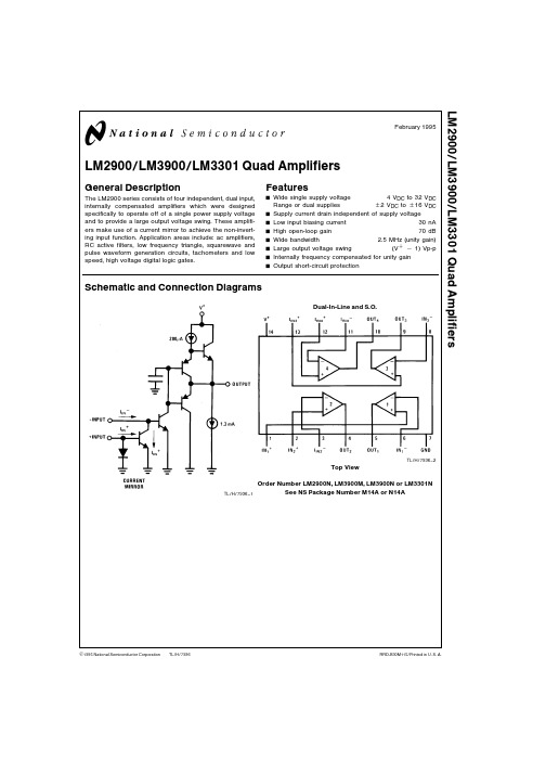
TL H 7936LM2900 LM3900 LM3301Quad AmplifiersFebruary 1995LM2900 LM3900 LM3301Quad AmplifiersGeneral DescriptionThe LM2900series consists of four independent dual input internally compensated amplifiers which were designed specifically to operate off of a single power supply voltage and to provide a large output voltage swing These amplifi-ers make use of a current mirror to achieve the non-invert-ing input function Application areas include ac amplifiers RC active filters low frequency triangle squarewave and pulse waveform generation circuits tachometers and low speed high voltage digital logic gatesFeaturesY Wide single supply voltage 4V DC to 32V DCRange or dual suppliesg 2V DC to g 16V DC Y Supply current drain independent of supply voltage Y Low input biasing current 30nA Y High open-loop gain 70dB Y Wide bandwidth 2 5MHz (unity gain)Y Large output voltage swing (V ab 1)Vp-p Y Internally frequency compensated for unity gain YOutput short-circuit protectionSchematic and Connection DiagramsTL H 7936–1Dual-In-Line and S OTL H 7936–2Top ViewOrder Number LM2900N LM3900M LM3900N or LM3301NSee NS Package Number M14A or N14AC 1995National Semiconductor Corporation RRD-B30M115 Printed in U S AAbsolute Maximum RatingsIf Military Aerospace specified devices are required please contact the National Semiconductor Sales Office Distributors for availability and specificationsLM2900 LM3900LM3301 Supply Voltage32V DC28V DCg16V DC g14V DC Power Dissipation(T A e25 C)(Note1)Molded DIP1080mW1080mWS O Package765mWInput Currents I IN a or I IN b20mA DC20mA DC Output Short-Circuit Duration One Amplifier Continuous ContinuousT A e25 C(See Application Hints)Operating Temperature Range b40 C to a85 C LM2900b40 C to a85 CLM39000 C to a70 CStorage Temperature Range b65 C to a150 C b65 C to a150 C Lead Temperature(Soldering 10sec )260 C260 C Soldering InformationDual-In-Line PackageSoldering(10sec )260 C260 C Small Outline PackageVapor Phase(60sec )215 C215 C Infrared(15sec )220 C220 CSee AN-450‘‘Surface Mounting Methods and Their Effect on Product Reliability’’for other methods of soldering surface mount devicesESD tolerance(Note7)2000V2000V Electrical Characteristics T A e25 C V a e15V DC unless otherwise statedParameter ConditionsLM2900LM3900LM3301Units Min Typ Max Min Typ Max Min Typ MaxOpen Voltage Gain Over TempV mV Loop Voltage Gain D V O e10V DC1 22 81 22 81 22 8Input Resistance Inverting Input111M XOutput Resistance889k XUnity Gain Bandwidth Inverting Input2 52 52 5MHzInput Bias Current Inverting Input V a e5V DC302003020030300nAInverting InputSlew Rate Positive Output Swing0 50 50 5V m s Negative Output Swing202020Supply Current R L e%On All Amplifiers6 2106 2106 210mA DCOutput V OUT High R L e2k I IN b e013 513 513 5Voltage V a e15 0V DC I IN a e0Swing VOUT Low I IN b e10m A0 090 20 090 20 090 2I IN a e0V DCV OUT High V a e Absolute I IN b e0Maximum Ratings I IN a e029 529 526 0R L e%Output Source618610518Current Sink(Note2)0 51 30 51 30 51 3mADC CapabilityI SINK V OL e1V I IN b e5m A5552Electrical Characteristics(Note6) V a e15V DC unless otherwise stated(Continued)Parameter ConditionsLM2900LM3900LM3301Units Min Typ Max Min Typ Max Min Typ MaxPower Supply Rejection T A e25 C f e100Hz707070dB Mirror Gain 20m A(Note3)0 901 01 10 901 01 10 9011 10m A m A 200m A(Note3)0 901 01 10 901 01 10 9011 10D Mirror Gain 20m A to200m A(Note3)252525% Mirror Current(Note4)105001050010500m A DC Negative Input Current T A e25 C(Note5)1 01 01 0mA DC Input Bias Current Inverting Input300300nA Note1 For operating at high temperatures the device must be derated based on a125 C maximum junction temperature and a thermal resistance of92 C W which applies for the device soldered in a printed circuit board operating in a still air ambient Thermal resistance for the S O package is131 C WNote2 The output current sink capability can be increased for large signal conditions by overdriving the inverting input This is shown in the section on Typical CharacteristicsNote3 This spec indicates the current gain of the current mirror which is used as the non-inverting inputNote4 Input V BE match between the non-inverting and the inverting inputs occurs for a mirror current(non-inverting input current)of approximately10m A This is therefore a typical design center for many of the application circuitsNote5 Clamp transistors are included on the IC to prevent the input voltages from swinging below ground more than approximately b0 3V DC The negative input currents which may result from large signal overdrive with capacitance input coupling need to be externally limited to values of approximately1mA Negative input currents in excess of4mA will cause the output voltage to drop to a low voltage This maximum current applies to any one of the input terminals If more than one of the input terminals are simultaneously driven negative smaller maximum currents are allowed Common-mode current biasing can be used to prevent negative input voltages see for example the‘‘Differentiator Circuit’’in the applications sectionNote6 These specs apply for b40 C s T A s a85 C unless otherwise statedNote7 Human body model 1 5k X in series with100pFApplication HintsWhen driving either input from a low-impedance source alimiting resistor should be placed in series with the inputlead to limit the peak input current Currents as large as20mA will not damage the device but the current mirror onthe non-inverting input will saturate and cause a loss of mir-ror gain at mA current levels especially at high operatingtemperaturesPrecautions should be taken to insure that the power supplyfor the integrated circuit never becomes reversed in polarityor that the unit is not inadvertently installed backwards in atest socket as an unlimited current surge through the result-ing forward diode within the IC could cause fusing of theinternal conductors and result in a destroyed unitOutput short circuits either to ground or to the positive pow-er supply should be of short time duration Units can bedestroyed not as a result of the short circuit current causingmetal fusing but rather due to the large increase in IC chipdissipation which will cause eventual failure due to exces-sive junction temperatures For example when operatingfrom a well-regulated a5V DC power supply at T A e25 C with a100k X shunt-feedback resistor(from the output tothe inverting input)a short directly to the power supply willnot cause catastrophic failure but the current magnitude willbe approximately50mA and the junction temperature willbe above T J max Larger feedback resistors will reduce thecurrent 11M X provides approximately30mA an open cir-cuit provides1 3mA and a direct connection from the out-put to the non-inverting input will result in catastrophic fail-ure when the output is shorted to V a as this then places thebase-emitter junction of the input transistor directly acrossthe power supply Short-circuits to ground will have magni-tudes of approximately30mA and will not cause cata-strophic failure at T A e25 CUnintentional signal coupling from the output to the non-in-verting input can cause oscillations This is likely only in breadboard hook-ups with long component leads and can be prevented by a more careful lead dress or by locating the non-inverting input biasing resistor close to the IC A quick check of this condition is to bypass the non-inverting input to ground with a capacitor High impedance biasing resis-tors used in the non-inverting input circuit make this input lead highly susceptible to unintentional AC signal pickupOperation of this amplifier can be best understood by notic-ing that input currents are differenced at the inverting-input terminal and this difference current then flows through the external feedback resistor to produce the output voltage Common-mode current biasing is generally useful to allow operating with signal levels near ground or even negative as this maintains the inputs biased at a V BE Internal clamp transistors(see note5)catch-negative input voltages at ap-proximately b0 3V DC but the magnitude of current flow has to be limited by the external input network For operation at high temperature this limit should be approximately100m A This new‘‘Norton’’current-differencing amplifier can be used in most of the applications of a standard IC op amp Performance as a DC amplifier using only a single supply is not as precise as a standard IC op amp operating with split supplies but is adequate in many less critical applications New functions are made possible with this amplifier which are useful in single power supply systems For example biasing can be designed separately from the AC gain as was shown in the‘‘inverting amplifier ’’the‘‘difference integra-tor’’allows controlling the charging and the discharging of the integrating capacitor with positive voltages and the‘‘fre-quency doubling tachometer’’provides a simple circuit which reduces the ripple voltage on a tachometer output DC voltage3Typical Performance CharacteristicsOpen Loop Gain Voltage Gain Voltage GainLarge Signal Frequency Input Current Supply Current ResponseOutput Sink Current Output Class-A Bias Current Output Source CurrentSupply Rejection Mirror Gain Maximum Mirror CurrentTL H 7936–94Typical Applications(V a e15V DC)Inverting AmplifierV ODC e V a 2A V j b R2R1TL H 7936–3Triangle Square GeneratorTL H 7936–4Frequency-Doubling TachometerTL H 7936–5Low V IN b V OUT Voltage RegulatorTL H 7936–6 Non-Inverting AmplifierV ODC e V a 2A V j R2R1TL H 7936–7Negative Supply BiasingV ODC eR2R3V bTL H 7936–8A V jR2R15Typical Applications (V a e 15V DC )(Continued)Low-Drift Ramp and Hold CircuitTL H 7936–10Bi-Quad Active Filter(2nd Degree State-Variable Network)TL H 7936–11Q e 50f O e 1kHz6Typical Applications(V a e15V DC)(Continued)Voltage-Controlled Current Source(Transconductance Amplifier)TL H 7936–12Hi V IN Lo(V IN b V O)Self-RegulatorQ1 Q2absorb Hi V INTL H 7936–13Ground-Referencing a Differential Input SignalTL H 7936–147Typical Applications(V a e15V DC)(Continued)Voltage Regulator(V O e V Z a V BE)TL H 7936–15Fixed Current SourcesI2e R1R2I1TL H 7936–16Voltage-Controlled Current Sink(Transconductance Amplifier)TL H 7936–17Buffer AmplifierV IN t V BETL H 7936–18TachometerTL H 7936–19V ODC e A f INAllows V O to go to zero8Typical Applications (V a e 15V DC )(Continued)Low-Voltage ComparatorNo negative voltage limit if properly biasedTL H 7936–20Power ComparatorTL H 7936–21Comparator TL H 7936–22Schmitt-TriggerTL H 7936–23Square-Wave Oscillator TL H 7936–24Pulse GeneratorTL H 7936–25Frequency Differencing TachometerV ODC e A (f 1b f 2)TL H 7936–269Typical Applications(V a e15V DC)(Continued)Frequency Averaging TachometerV ODC e A(f1a f2)TL H 7936–27Squaring Amplifier(W Hysteresis)TL H 7936–28Bi-Stable MultivibratorTL H 7936–29Differentiator(Common-Mode Biasing Keeps Input at a V BE)A V e 1 2TL H 7936–30‘‘OR’’Gatef e A a B a CTL H 7936–31‘‘AND’’Gatef e A B CTL H 7936–32Difference IntegratorTL H 7936–33 10Typical Applications (V a e 15V DC )(Continued)Low Pass Active Filterf O e 1kHzTL H 7936–34Staircase GeneratorTL H 7936–35V BE BiasingA V j bR2R1TL H 7936–36Bandpass Active FilterTL H 7936–37f o e 1kHz Q e 2511Typical Applications(V a e15V DC)(Continued)Low-Frequency MixerTL H 7936–38Free-Running Staircase Generator Pulse CounterTL H 7936–3912Typical Applications(V a e15V DC)(Continued)Supplying I IN with Aux Amp(to Allow Hi-Z Feedback Networks)TL H 7936–40One-Shot MultivibratorPW j2c106CSpeeds recoveryTL H 7936–41Non-Inverting DC Gain to(0 0)TL H 7936–4213Typical Applications(V a e15V DC)(Continued)Channel Selection by DC Control(or Audio Mixer)TL H 7936–4314Typical Applications (V a e 15V DC )(Continued)Power AmplifierTL H 7936–44One-Shot with DC Input ComparatorTL H 7936–45Trips at V IN j 0 8VaV IN must fall 0 8Vaprior to t 2High Pass Active FilterTL H 7936–4615Typical Applications(V a e15V DC)(Continued)Sample-Hold and Compare with New a V INTL H 7936–47Sawtooth GeneratorTL H 7936–4816Typical Applications(V a e15V DC)(Continued)Phase-Locked LoopTL H 7936–49Boosting to300mA LoadsTL H 7936–5017Split-Supply Applications(V a e a15V DC V b e b15V DC)Non-Inverting DC GainTL H 7936–51AC AmplifierTL H 7936–5218Physical Dimensions inches(millimeters)Small Outline Package(M)Order Number LM3900MNS Package Number M14A19L M 2900 L M 3900 L M 3301Q u a d A m p l i f i e r sPhysical Dimensions inches (millimeters)(Continued)Molded Dual-In-Line Package (N)Order Number LM2900N LM3900N or LM3301NNS Package Number N14ALIFE SUPPORT POLICYNATIONAL’S PRODUCTS ARE NOT AUTHORIZED FOR USE AS CRITICAL COMPONENTS IN LIFE SUPPORT DEVICES OR SYSTEMS WITHOUT THE EXPRESS WRITTEN APPROVAL OF THE PRESIDENT OF NATIONAL SEMICONDUCTOR CORPORATION As used herein 1 Life support devices or systems are devices or 2 A critical component is any component of a life systems which (a)are intended for surgical implant support device or system whose failure to perform can into the body or (b)support or sustain life and whose be reasonably expected to cause the failure of the life failure to perform when properly used in accordance support device or system or to affect its safety or with instructions for use provided in the labeling can effectivenessbe reasonably expected to result in a significant injury to the userNational Semiconductor National Semiconductor National Semiconductor National Semiconductor CorporationEuropeHong Kong LtdJapan Ltd1111West Bardin RoadFax (a 49)0-180-530858613th Floor Straight Block Tel 81-043-299-2309。
步进电机驱动原理及应用程序
∙ULN2003步进电机驱动原理及应用程序∙发布时间:2011-5-9 10:38:11 | 来源: 第一价值网| 查看: 1191次| 收藏| 打印TAG:ULN2003 步进电机驱动 ULN2003原理 ULN2003应用程序步进电机的基本原理我就不说了,百度能找出一大片来,,简而言之就是能够通过输入脉冲的个数,确定旋转的角位移,一般用他来控制小车轮子的偏移角度等。
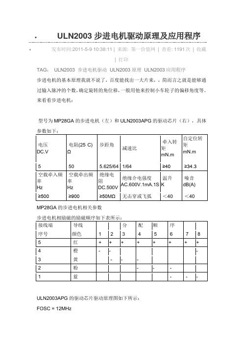
来看看步进电机:型号为MP28GA的步进电机(左)和ULN2003APG的驱动芯片(右),具体参数如下:电压DC.V电阻(25°C)Ω步距角°减速比牵入转矩mN.m自定位转矩mN.m5 50 5.625/64 1/64 ≥40≥34.3空载牵入频率Hz空载牵出频率Hz绝缘电阻DC.500V绝缘介电强度AC.600V.1mA.1S温升K噪音dB(A)≥500≥900≥50MΩ无击穿或飞弧<40 <40 MP28GA的步进电机相关参数接线端导线分配顺序序号颜色 1 2 3 4 5 6 7 8 5 红 + + + + + + + + 4 橙 - - - 3 黄 - - -2 粉- - -1 蓝 - - -ULN2003APG的驱动芯片驱动原理图如下所示:FOSC = 12MHz说得通俗uln2003相当于继电器的作用,例如7个继电器的一端连某电压[也即uln2003电源电压](<50)在一起,而另一端作为则作为输出,又好如一个二极管,只不过因电路集成功能的因素,输出的电压等同于uln2003的电压罢了,常用于步进电机;--------------------------------------------------; 步进电机的驱动信号必须为脉冲信号!!! 转动的速度和脉冲的频率成正比!!!; 本步进电机步进角为5.625度 . 一圈360 度, 需要64个脉冲完成!!!;--------------------------------------------------; A组线圈对应P2.4; B组线圈对应P2.5; C组线圈对应P2.6; D组线圈对应P2.7; 正转次序: AB组--BC组--CD组--DA组(即一个脉冲,正转5.625度);------------------------------------------------ORG 0000HLJMP MAINORG 0100HMAIN:;----------------------------正转MOV R3,#192 ;正转3圈共192个脉冲START:MOV R0,#00HSTART1:MOV P2,#00HMOV A,R0MOV DPTR,#TABLEMOVC A,@A+DPTRJZ START ;对A的判断,当A=0时则转到START MOV P2,ALCALL DELAYINC R0DJNZ R3,START1MOV P2,#00HLCALL DELAY1;-----------------------------反转MOV R3,#64 ;反转一圈共64个脉冲START2:MOV P2,#00HMOV R0,#05START3:MOV A,R0MOV DPTR,#TABLEMOVC A,@A+DPTRJZ START2MOV P2,ACALL DELAYINC R0DJNZ R3,START3MOV P2,#00HLCALL DELAY1LJMP MAIN;---------------------------转速控制DELAY: MOV R7,#40 ;步进电机的转速M3: MOV R6,#248DJNZ R6,$DJNZ R7,M3RET;---------------------------延时控制DELAY1: MOV R4,#20 ;2S 延时子程序DEL2: MOV R3,#200DEL3: MOV R2,#250DJNZ R2,$DJNZ R3,DEL3DJNZ R4,DEL2RET;---------------------------正反转表TABLE:DB 30H,60H,0C0H,90H; 正转表DB 00; 正转结束DB 30H,90H,0C0H,60H; 反转表DB 00; 反转结束END/**************************************//*杭州电子&计算机工作室*//* *//*步进电机演示程*//*目标器件:AT89S51 *//*晶振:11.0592MHZ *//*编译环境:Keil 7.50A *//****************************//*************包含头文件*******/#include/**************端口定义****************/ sbit key = P1^4;/*********************************函数功能:延时子程序入口参数:出口参数:*****************************************/ void delay(void){int k;for(k=0;k<500;k++);}/*************************************函数功能:主程序入口参数:出口参数:********************************/void main(){P1=0x00; //输出全高key=1; //按键置输入状态while(1) //主循环{if(key==1) //无键按下正转{P1=0xFC; //1100delay();P1=0xF6; //0110delay();P1=0xF3; //0011delay();P1=0xF9; //1001delay();}else //有键按下反转{P1=0xFC; //1100delay();P1=0xF9; //1001delay();P1=0xF3; //0011delay();P1=0xF6; //0110delay();}}}1.步进电机是将电脉冲信号转变为角位移或线位移的开环控制元件。
LM1893应用实例
0 引言低压电力线(220V或380V交流供电线路)随处可见,利用现成的低压电力线来传输信号具有有线通信的优点,而又无需再另行架杆、拉线、凿墙,可以充分利用已有的线路资源,降低通信成本。
电力线载波通信技术可广泛应用于工业自动控制系统,电能管理系统,家用电器控制系统,防火报警系统及计算机终端接口等场合。
本文要介绍的LM1893就是一种能够直接驱动常规电力线的集成芯片。
1 LM1893的功能特点LM1893芯片是美国国家半导体公司生产的专用电力载波通信芯片,该芯片价格低廉,使用方便,精度高,可靠性好,可以实现任意编码方式的数字序列的半双工通信,其特性如下:(1)抑制噪声的FSK调制方式(2)传输速率最高达4.8KBaud(3)载波频率在50kHz至300kHz之间可选择(4)在数据中允许存在“0”、“1”串(5) TTL和MOS数字电平兼容(6)能驱动常规电力线(7)接收灵敏度2mV2 LM1893的内部结构及工作原理LM1893的内部结构如图1所示。
LM1893分为发送和接收两部分。
数据的发送部分由FSK调制器、电流控制振荡器、正弦波发生器、输出放大器及自动电平控制电路(ALC)构成。
接收部分由限幅放大器、锁相环信号解调器、低通滤波器、直流消除电路及噪声滤波电路构成。
电路的发送与接收工作状态由芯片引脚TX/ 控制端切换。
当TX/ 为高电平时,LM1893工作于发送模式下,要发送的数据送入芯片内的FSK调制器,产生开关控制电流,驱动电流控制振荡器产生2.2%频偏的三角波,三角波经过正弦波发生器形成已调正弦波信号,经由输出放大器驱动后输出到线路耦合电路,再发送到电力线上。
电力线路上的负载情况复杂,当某种原因促使输出幅度超过额定电平时,ALC电路能够有效地控制输出放大器的输出幅度,使其输出电平保持在稳定范围之内。
当TX/ 为低电平时,LM1893工作于接收模式,经线路耦合电路送来的已调载波信号送入芯片的I/O端口,由平衡限幅器放大,取出信号中的直流分量并对耦合进来的工频信号衰减,送入差分锁相环路,解调出数据信号。
LM298驱动直流电机

设计说明书题目:直流电机控制专业:机电班级:机械111姓名:蒋德昌学号:2011071117摘要随着时代发展,电动机作为最主要的机电能量转换装置,其应用已普及国民经济和人们日常生活,据资料显示,在所有的动力资源中,百分之九十以上的动力来源来自电动机,而在我国,电能百分之六十用于电动机,种种数据表明了电动机的重要性。
本次设计是基于51内核的单片机设计,采用LM298直流电机驱动器,并采用LCD1602液晶显示电动机的转向和转速,采用PWM调速方式,通过改变PWM占空比从而改变电动机的电枢电压,进而实现对电动机的调速。
通过按键改变,由程序控制电机两端电压的变化,进而实现对电机转向的控制。
软件上采用proteus设计原理图,采用C语言编写程序,之后进行模拟仿真。
在编写程序是将程序模块化,便于程序的编写。
本次整体设计,采用了大量的集成电路模块,简化了硬件电路,提高了系统的稳定性和可靠性,使得整个系统的性能得到保证。
关键字:电动机、LM298、PWM调速、集成电路。
目录1设计任务 (4)2系统整体方案 (4)3仿真图 (6)4所用硬件介绍 (7)4.1 L298驱动电路 (7)4.2 LCD1602 (8)4.3排阻 (9)仿真图: (9)4.4 直流电机 (10)4.5按键 (11)5软件系统设计 (12)5.1 主程序流程图 (12)5.2电机方向改变的设计 (12)5.3电机转速的设计 (13)6总结 (14)1设计任务通过298驱动模块驱动两个直流电机,并通过改变PWM占空比和电机两端电压实现对电动机的调速、调向。
采用LCD1602显示电机的转速和转向。
(1)按下按键1,电机A改变转动方向,LCD1602上面第一行显示此时电机的转向。
(2)按下按键2,电机A改变转速,每按一下,电机A的转速提高,LCD1602上面第一行显示转速等级。
(3)按下按键3,电机B改变转动方向,LCD1602上面第二行显示此时电机的转向。
电机驱动LM298课件

步进电机驱动实例
总结词
精确控制,适用于需要高精度定位的场合。
详细描述
步进电机是一种通过脉冲信号控制的电机,能够实现精确的定位和速度控制。使用LM298驱动步进电机时,可以 通过控制脉冲信号的频率和数量来实现电机的转动角度和速度。这种控制方式适用于需要高精度定位的场合,如 数控机床、打印机等。
伺服电机驱动实例
电机。
通过PWM(脉冲宽度调制)控 制信号,LM298可以调节电机
的转速和方向。
LM298内置保护功能,如过流 保护和过热保护,能够提高系统
的稳定性和安全性。
LM298的优势与局限性
01
优势
02
高电压、大电流输出能力,适用于驱动多种类 型的电机。
03
内置保护功能,提高系统安全性。
LM298的优势与局限性
问题2
电机转动方向不对。解决方案:检查 输入信号的相位是否正确,可以通过 调整输入信号的顺序来改变电机的转 动方向。
05
电机驱动LM298的应用实 例
直流电机驱动实例
总结词
简单易用,适用于小型直流电机驱动。
详细描述
LM298是一款常见的电机驱动芯片,常用于直流电机驱动。它具有简单的控制方 式,只需通过PWM信号调节电机速度,同时支持正反转控制。由于其简单易用 ,广泛应用于小型直流电机驱动,如玩具车、无人机等。
连接方式
LM298的电源引脚应连接到适当的电 源,通常为直流电源。同时,输入和 输出引脚应连接到相应的电路中,以 实现电机的驱动和控制。
调试步骤与注意事项
调试步骤
首先,检查LM298的电源是否正常,确保电源电压在规定范围内。然后,检查 输入和输出引脚的信号是否正常,可以使用示波器或逻辑分析仪进行检测。
LF298中文资料

LM2904V中文资料

Industrial Temperature Range (– 25°C to +85°C) LM201A 0.075 2.0 10 10 50 1.0 0.5 General Purpose N/626, D/751
Internally Compensated
Commercial Temperature Range (0°C to +70°C) LF351 LF411C MC1436, C MC1741C MC1776C MC3476 MC34001 MC34001B MC34071 MC34071A MC34080B MC34081B MC34181 TL071AC TL071C TL081AC TL081C 200 pA 200 pA 0.04 0.5 0.003 0.05 200 pA 200 pA 0.5 500 nA 200 pA 200 pA 0.1 nA 200 pA 200 pA 200 pA 400 pA 10 2.0 10 6.0 6.0 6.0 10 5.0 5.0 3.0 1.0 1.0 2.0 6.0 10 6.0 15 10 10 12 15 15 15 10 10 10 10 10 10 10 10 10 10 10 100 pA 100 pA 10 200 3.0 25 100 pA 100 pA 75 50 100 pA 100 pA 0.05 50 pA 50 pA 100 pA 200 pA 25 25 70 20 100 50 25 50 25 50 25 25 25 50 25 50 25 4.0 8.0 1.0 1.0 1.0 1.0 4.0 4.0 4.5 4.5 16 8.0 4.0 4.0 4.0 4.0 4.0 13 25 2.0 0.5 0.2 0.2 13 13 10 10 55 30 10 13 13 13 13 ±5.0 +5.0 ±15 ±3.0 ±1.2 ±1.5 ±5.0 ±5.0 +3.0 +3.0 ±5.0 ±5.0 ±2.5 ±5.0 ±5.0 ±5.0 ±5.0 ±18 ±22 ±34 ±18 ±18 ±18 ±18 ±18 +44 +44 ±22 ±22 ±18 ±18 ±18 ±18 ±18 JFET Input JFET Input, Low Offset, Low Drift High Voltage General Purpose µPower, Programmable Low Cost, µPower, Programmable JFET Input JFET Input High Performance Single Supply Decompensated High Speed, JFET Input Low Power, JFET Input Low Noise, JFET Input Low Noise, JFET Input JFET Input JFET Input N/626, D/751 N/626, D/751 P1/626, D/751 P1/626, D/751 P1/626, D/751 P1/626 P/626, D/751 P/626, D/751 P/626, D/751 P/626, D/751 P/626, D/751 P/626, D/751 P/626 P/626 D/751 P/626 D/751
- 1、下载文档前请自行甄别文档内容的完整性,平台不提供额外的编辑、内容补充、找答案等附加服务。
- 2、"仅部分预览"的文档,不可在线预览部分如存在完整性等问题,可反馈申请退款(可完整预览的文档不适用该条件!)。
- 3、如文档侵犯您的权益,请联系客服反馈,我们会尽快为您处理(人工客服工作时间:9:00-18:30)。
L298Jenuary 2000DUAL FULL-BRIDGE DRIVERMultiwatt15ORDERING NUMBERS :L298N (Multiwatt Vert.)L298HN (Multiwatt Horiz.)L298P (PowerSO20)BLOCK DIAGRAM.OPERATING SUPPLY VOLTAGE UP TO 46V .TOTAL DC CURRENT UP TO 4A .LOW SATURATION VOLTAGE.OVERTEMPERATURE PROTECTION.LOGICAL ”0”INPUT VOLTAGE UP TO 1.5V (HIGH NOISE IMMUNITY)DESCRIPTIONThe L298is an integrated monolithic circuit in a 15-lead Multiwatt and PowerSO20packages.It is a high voltage,high current dual full-bridge driver de-signedto acceptstandardTTL logic levels anddrive inductive loads such as relays,solenoids,DC and steppingmotors.Two enableinputs are provided to enableor disablethe deviceindependentlyof thein-put signals.The emitters of the lower transistors of each bridge are connected togetherand the corre-sponding external terminal can be used for the con-nectionof an externalsensing resistor.Anadditional supply input is provided so that the logic works at a lower voltage.PowerSO20®1/13PIN CONNECTIONS (top view)GND Input 2VSS N.C.Out 1V S Out 2Input 1Enable A Sense AGND1089765432131415161719182012111GNDD95IN239Input 3Enable B Out 3Input 4Out 4N.C.Sense B GND ABSOLUTE MAXIMUM RATINGSSymbol ParameterValue Unit V S Power Supply 50V V SS Logic Supply Voltage 7V V I ,V en Input and Enable Voltage–0.3to 7V I OPeak Output Current (each Channel )–Non Repetitive (t =100µs)–Repetitive (80%on –20%off;t on =10ms)–DC Operation 32.52A A A V sens Sensing Voltage–1to 2.3V P tot Total Power Dissipation (T case =75°C)25W T op Junction Operating Temperature –25to 130°C T stg ,T jStorage and Junction Temperature–40to 150°CTHERMAL DATASymbol ParameterPowerSO20Multiwatt15Unit R th j-case Thermal Resistance Junction-case Max.–3°C/W R th j-ambThermal Resistance Junction-ambientMax.13(*)35°C/W(*)Mounted on aluminum substrate1234567910118ENABLE B INPUT 3LOGIC SUPPLY VOLTAGE V SS GND INPUT 2ENABLE A INPUT 1SUPPLY VOLTAGE V S OUTPUT 2OUTPUT 1CURRENT SENSING ATAB CONNECTED TO PIN 813141512CURRENT SENSING B OUTPUT 4OUTPUT 3INPUT 4D95IN240AMultiwatt15PowerSO20L2982/13PIN FUNCTIONS(refer to the block diagram)MW.15PowerSO Name Function1;152;19Sense A;Sense B Between this pin and ground is connected the sense resistor tocontrol the current of the load.2;34;5Out1;Out2Outputs of the Bridge A;the current that flows through the loadconnected between these two pins is monitored at pin1.46V S Supply Voltage for the Power Output Stages.A non-inductive100nF capacitor must be connected between thispin and ground.5;77;9Input1;Input2TTL Compatible Inputs of the Bridge A.6;118;14Enable A;Enable B TTL Compatible Enable Input:the L state disables the bridge A(enable A)and/or the bridge B(enable B).81,10,11,20GND Ground.912VSS Supply Voltage for the Logic Blocks.A100nF capacitor must beconnected between this pin and ground.10;1213;15Input3;Input4TTL Compatible Inputs of the Bridge B.13;1416;17Out3;Out4Outputs of the Bridge B.The current that flows through the loadconnected between these two pins is monitored at pin15.–3;18N.C.Not ConnectedELECTRICAL CHARACTERISTICS(V S=42V;V SS=5V,T j=25°C;unless otherwise specified)Symbol Parameter Test Conditions Min.Typ.Max.Unit V S Supply Voltage(pin4)Operative Condition V IH+2.546V V SS Logic Supply Voltage(pin9) 4.557VI S Quiescent Supply Current(pin4)V en=H;I L=0V i=LV i=H 13502270mAmAV en=L V i=X4mAI SS Quiescent Current from V SS(pin9)V en=H;I L=0V i=LV i=H 2473612mAmAV en=L V i=X6mA V iL Input Low Voltage(pins5,7,10,12)–0.3 1.5VV iH Input High Voltage(pins5,7,10,12)2.3VSS VI iL Low Voltage Input Current(pins5,7,10,12)V i=L–10µAI iH High Voltage Input Current(pins5,7,10,12)Vi=H≤V SS–0.6V30100µA V en=L Enable Low Voltage(pins6,11)–0.3 1.5V V en=H Enable High Voltage(pins6,11) 2.3V SS V I en=L Low Voltage Enable Current(pins6,11)V en=L–10µAI en=H High Voltage Enable Current(pins6,11)V en=H≤V SS–0.6V30100µAV CEsat(H)Source Saturation Voltage I L=1AI L=2A 0.95 1.3521.72.7VVV CEsat(L)Sink Saturation Voltage I L=1A(5)I L=2A(5)0.85 1.21.71.62.3VVV CEsat Total Drop I L=1A(5)I L=2A(5)1.80 3.24.9VVV sens Sensing Voltage(pins1,15)–1(1)2VL2983/13Figure 1:Typical Saturation Voltage vs.OutputCurrent.Figure 2:Switching Times Test Circuits.Note :For INPUT Switching,set EN =HFor ENABLESwitching,set IN =H1)1)Sensing voltage can be –1V for t ≤50µsec;in steady state V sens min ≥–0.5V.2)See fig.2.3)See fig.4.4)The load must be a pure resistor.ELECTRICAL CHARACTERISTICS (continued)Symbol ParameterTest ConditionsMin.Typ.Max.Unit T 1(V i )Source Current Turn-off Delay 0.5V i to 0.9I L (2);(4) 1.5µs T 2(V i )Source Current Fall Time 0.9I L to 0.1I L (2);(4)0.2µs T 3(V i )Source Current Turn-on Delay 0.5V i to 0.1I L (2);(4)2µs T 4(V i )Source Current Rise Time 0.1I L to 0.9I L (2);(4)0.7µs T 5(V i )Sink Current Turn-off Delay 0.5V i to 0.9I L (3);(4)0.7µs T 6(V i )Sink Current Fall Time 0.9I L to 0.1I L (3);(4)0.25µs T 7(V i )Sink Current Turn-on Delay 0.5V i to 0.9I L (3);(4) 1.6µs T 8(V i )Sink Current Rise Time 0.1I L to 0.9I L (3);(4)0.2µs fc (V i )Commutation Frequency I L =2A 2540KHz T 1(V en )Source Current Turn-off Delay 0.5V en to 0.9I L (2);(4)3µs T 2(V en )Source Current Fall Time 0.9I L to 0.1I L (2);(4)1µs T 3(V en )Source Current Turn-on Delay 0.5V en to 0.1I L (2);(4)0.3µs T 4(V en )Source Current Rise Time 0.1I L to 0.9I L (2);(4)0.4µs T 5(V en )Sink Current Turn-off Delay 0.5V en to 0.9I L (3);(4) 2.2µs T 6(V en )Sink Current Fall Time 0.9I L to 0.1I L (3);(4)0.35µs T 7(V en )Sink Current Turn-on Delay 0.5V en to 0.9I L (3);(4)0.25µs T 8(V en )Sink Current Rise Time0.1I L to 0.9I L(3);(4)0.1µsL2984/13L298 Figure3:Source Current Delay Times vs.Input or Enable Switching.Figure4:Switching Times Test Circuits.Note:For INPUT Switching,set EN=HFor ENABLE Switching,set IN=L5/13L298Figure5:Sink Current Delay Times vs.Input0V Enable Switching.Figure6:Bidirectional DC Motor Control.Inputs FunctionV en=H C=H;D=L ForwardC=L;D=H ReverseC=D Fast Motor StopV en=L C=X;D=X Free RunningMotor StopL=Low H=High X=Don’t care6/13Figure7:For higher currents,outputs can be paralleled.Take care to parallel channel1with channel4 and channel2with channel3.APPLICATION INFORMATION(Refer to the block diagram)1.1.POWER OUTPUT STAGETheL298integratestwopoweroutputstages(A;B). The power output stage is a bridge configuration and its outputs can drive an inductive load in com-mon or differenzialmode,dependingon thestate of the inputs.The current that flows through the load comes out from the bridge at the sense output:an externalresistor(R SA;R SB.)allows to detect the in-tensity of this current.1.2.INPUT STAGEEach bridge is driven by means of four gatesthe in-put of which are In1;In2;EnA and In3;In4;EnB. The In inputsset thebridge state when The En input is high;a lowstateof theEn inputinhibitsthe bridge. All the inputs are TTL compatible.2.SUGGESTIONSA non inductive capacitor,usually of100nF,must be foreseen between both Vs and Vss,to ground, as near as possible to GND pin.When the large ca-pacitor of the power supply is too far from the IC,a second smaller one must be foreseen near the L298.The sense resistor,not of a wire wound type,must be groundednear the negative pole of Vs that must be near the GND pin of the I.C.Each input must be connected to the source of the driving signals by means of a very short path. Turn-On and Turn-Off:Before to Turn-ONthe Sup-plyVoltageand beforeto Turnit OFF,the Enablein-put must be driven to the Low state.3.APPLICATIONSFig6shows a bidirectional DC motor controlSche-matic Diagram for which only one bridge is needed. The external bridge of diodes D1to D4is made by four fast recovery elements(trr≤200nsec)that must be chosen of a VF as low as possible at the worst case of the load current.The senseoutputvoltage can be used to controlthe current amplitude by chopping the inputs,or to pro-vide overcurrent protection by switching low the en-able input.The brake function(Fast motor stop)requires that the Absolute Maximum Rating of2Amps must never be overcome.When the repetitive peak current needed from the load is higher than2Amps,a paralleled configura-tion can be chosen(See Fig.7).An external bridge of diodes are required when in-ductive loads are driven and when the inputs of the ICare chopped;Shottkydiodeswould bepreferred.L2987/13This solution can drive until3AmpsIn DC operation and until3.5Amps of a repetitive peak current. OnFig8it is shownthedriving ofa twophasebipolar stepper motor;the needed signals to drive the in-puts of the L298are generated,in this example, from the IC L297.Fig9shows an example of P.C.B.designed for the application of Fig8.Fig10shows a second two phase bipolar stepper motor control circuit where the current is controlled by the I.C.L6506.Figure8:Two Phase Bipolar Stepper Motor Circuit.This circuit drives bipolar stepper motors with winding currents up to2A.The diodes are fast2A types.R S1=R S2=0.5ΩD1to D8=2A Fast diodes{V F≤1.2V@I=2Atrr≤200nsL2988/13L298 Figure9:SuggestedPrinted Circuit Board Layout for the Circuit of fig.8(1:1scale).Figure10:Two Phase Bipolar Stepper Motor Control Circuit by Using the Current Controller L6506.R R and R sense depend from the load current9/13Multiwatt15VDIM.mminch MIN.TYP.MAX.MIN.TYP.MAX.A 50.197 B 2.650.104C 1.60.063D 10.039E 0.490.550.0190.022F 0.660.750.0260.030G 1.02 1.27 1.520.0400.0500.060G117.5317.7818.030.6900.7000.710H119.60.772H220.20.795L 21.922.222.50.8620.8740.886L121.722.122.50.8540.8700.886 L217.6518.10.6950.713 L317.2517.517.750.6790.6890.699L410.310.710.90.4060.4210.429L7 2.65 2.90.1040.114M 4.25 4.55 4.850.1670.1790.191M1 4.63 5.08 5.530.1820.2000.218S 1.9 2.60.0750.102S1 1.9 2.60.0750.102Dia13.653.850.1440.152OUTLINE AND MECHANICAL DATAL29810/13DIM.mm inchMIN.TYP.MAX.MIN.TYP.MAX.A50.197B 2.650.104C 1.60.063 E0.490.550.0190.022 F0.660.750.0260.030 G 1.14 1.27 1.40.0450.0500.055 G117.5717.7817.910.6920.7000.705 H119.60.772H220.20.795 L20.570.810L118.030.710L2 2.540.100L317.2517.517.750.6790.6890.699 L410.310.710.90.4060.4210.429 L5 5.280.208L6 2.380.094L7 2.65 2.90.1040.114S 1.9 2.60.0750.102 S1 1.9 2.60.0750.102 Dia1 3.65 3.850.1440.152Multiwatt15HOUTLINE AND MECHANICAL DATAL29811/13JEDEC MO-166PowerSO20ea2AEa1PSO20MECDETAIL ATD11120E1E2h x 45DETAIL Aleadsluga3SGage Plane0.35LDETAIL BRDETAIL B(COPLANARITY)GC-C -SEATING PLANEe3bcNN HBOTTOM VIEWE3D1DIM.mm inch MIN.TYP.MAX.MIN.TYP.MAX.A 3.60.142a10.10.30.0040.012 a2 3.30.130 a300.10.0000.004b 0.40.530.0160.021c 0.230.320.0090.013D (1)15.8160.6220.630D19.49.80.3700.386E 13.914.50.5470.570e 1.270.050e311.430.450E1(1)10.911.10.4290.437E2 2.90.114 E3 5.8 6.20.2280.244G 00.10.0000.004H 15.515.90.6100.626h 1.10.043 L 0.81.10.0310.043N 10°(max.)S T100.394(1)”D and F”do not include mold flash or protrusio ns.-Mold flash or protrus ions shall not exceed 0.15mm (0.006”).-Criticaldimensions :”E”,”G”and ”a3”OUTLINE AND MECHANICAL DATA8°(max.)10L29812/13L298 Information furnished is believed to be accurate and reliable.However,STMicroelectronics assumes no responsibility for the conse-quences of use of such information nor for any infringement of patents or other rights of third parties which may result from its use.No license is granted by implication or otherwise under any patent or patent rights of STMicroelectronics.Specification mentioned in this publication are subject to change without notice.This publication supersedes and replaces all information previously supplied.STMi-croelectronics products are not authorized for use as critical components in life support devices or systems without express written approval of STMicroelectronics.The ST logo is a registered trademark of STMicroelectronics©2000STMicroelectronics–Printed in Italy–All Rights ReservedSTMicroelectronics GROUP OF COMPANIESAustralia-Brazil-China-Finland-France-Germany-Hong Kong-India-Italy-Japan-Malaysia-Malta-Morocco-Singapore-Spain-Sweden-Switzerland-United Kingdom-U.S.A.13/13。