MIC4100中文资料
MIC总线技术简介
2)MIC总线的数据格式 命令和响应都是32位曼彻斯特码
三、MIC总线电气特性
•RS-485的电气特性:逻辑“1”以两线间 的电压差为+(2~6)V表示;逻辑“0”以两线 间的电压差为-(2~6)V表示。接口信号电平 比RS-232-C降低了,就不易损坏接口电路 的芯片, 且该电平与TTL电平兼容,可方 便与TTL电路连接。
MIC典型芯片可以被设置为四种工作模 式:
1、处理器接口模式PIM; 2、远程开关模式RSM; 3、数据输入模式DIM; 4、数据输出模式DOM;
当总线芯片设置为处理器接口模式 (PIM)时,即成为总线控制器
2、MIC总线的协议
1)指令概述 MIC协议由9种基本指令组成:
设置指令、自检指令、检取模块指令、包含数据 字的执行指令、检取单一设备指令、 检取单一数据设备指令、检取多设备指令、 检取多数据设备指令、广播指令(无需响应)
MIC总线是专门为解决恶劣的军事环境(包括 核辐射)中电力及数据分配和管理问题而开发 的一种简单可靠性时间分割多路传输串线控制器或遥控模块,独立实 现串行远程控制; 2、相对于1553B总线,具有便宜、简单性能高的特点,具 有完备的检错体系; 3、命令/响应协议,具有完备的检错体系; 4、远程模块工作无需微处理器; 5、双路数据总线冗余 6、总线控制器与备用总线控制器易实现冗余控制; 7、总线最大传输速率为2.0Mb/s 8、总线寻址64个远程模块,每个远程模块直接寻址32个设 备; 9、信息长度:3位同步;32位数据,1位校验; 10、可用于环境恶劣的军事环境
拓扑结构
• MIC总线系统包括总线控制器、远程模块两个基 本部分组成,同时在两条总线上传输数据。
二、通信原理
MIC总线为命令/响应操作,总线控制器以 传输一个命令到一个特定的远程模块。所有远 程模块接受和判断这个命令,硬件链接地址与 命令中特定模块地址相同的模块将立即通过串 行总线传回相应的响应消息。总线控制器收到 响应并让相关的数据或总线消息传回微处理器。
CV-3100、CV-4100三丰轮廓仪中文样本
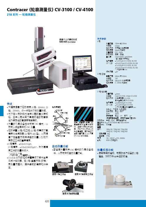
• 驱动装置 (X 轴) 和立柱 (Z2 轴) 中集成了高 精度线性编码器 (Z2 轴为 ABS 型),从而提 高了在垂直方向持续自动测量小孔和不 易定位工件的重复精度。
• X 轴精度:±(0.8+0.01L)µm, Z1 轴精度:±(0.8+|0.5H|/25)µm*,针对高精 度工件的测量所设计。
基座尺寸 (W x H):750 x 600mm 或 1000 x 450mm
基座材料 : 花岗岩
重量
主机 :
140kg (S4), 150kg (H4), 155kg (W4)
145kg (S8), 155kg (H8), 160kg (W8)
控制装置 :14kg
遥控箱 : 0.9kg
电源 :
测量控制 轮廓分析功能
性能参数
型号 货号 (mm) 货号 (inch)
型号 货号 (mm) 货号 (inch) X1 轴测量范围 垂直行程 花岗岩基座尺寸 (WxD) 尺寸 (主机、WxDxH) 重量 (主机)
CV-3100S4 218-421* 218-431*
CV-4100S4 218-461* 218-471* 100mm 300mm 电动立柱 600 x 450mm 741 x 450 x 905mm 140kg
CV-3100H4 218-422* 218-432*
CV-4100H4 218-462* 218-472* 100mm 500mm 电动立柱 600 x 450mm 741 x 450 x 1105mm 150kg
型号 货号 (mm) 货号 (inch)
CV-3100S8 218-426* 218-436*
SERVOMEX4100操作说明书
1.2:手册的范围本手册涵盖了软件设置和操作。
更多的复本可供订购,订购编号为04000/003C。
•获取技术支持及备件的联系方式请见本手册封底。
•随仪器提供一份安装手册,内容包括了技术指标、日常维护和备件信息,订购编号为04000/005C。
•维护手册是专为专业技术人员而编写的,购编号为04000/002C警告用户应当注意到Xentra仪器内部没有需要用户维护的部件。
仪器外壳保护用户免遭电击或其它危害。
所有维护工作应当由专业技术人员进行。
图A分析仪正视图1.样气过滤器(可选) 4.键盘2.流量计(可选) 5 .显示对比度调节3.显示6.样气调节针阀(可选) 图BXentra的显示1.标题7.报警图标2.模块位置(2字符) 8.预热图标3.测量值(6字符) 9.自动标定图标4.工程单位(3字符) 10.维护图标5.组份名称(6字符) 11.故障图标6.测量显示条目图C自动标定的典型时序(示例中,标气1为零点气,标气2为量程气) 1.自动标定开始,标气1通入分析仪2.标气1测量中3.标气2通入分析仪4.标气2测量中5.标气1再次通入分析仪6.再次测量标气17.样气体通入分析仪吹扫传感器(后吹扫)图D用户界面菜单结构图1概述11.1警告、注意和提示 11.2手册的范围 11.3用户界面介绍 42初始设置72.1开机和关机步骤72.2分析仪功能的一般操作72.3设定密码82.4设定时间和日期83主要设置93.1组份名称和单位的定义93.2报警10 3.3继电器的分配 11 3.4外部模拟量输入的设置 133.5模拟量输出 133.6定义和选择测量显示屏幕 15 3.7响应时间 16 3.8串行通讯输出163.9氮氧化物(NOx)浓度的计算17 4标定 184.1标定简介 18 4.2设定低点和高点标定的允许误差 19 4.3手动标定和检查19 4.4顺磁模块压力传感器的标定 22 4.5自动标定和自动检查的设置 24 5查看配置和历史文件 285.1显示当前的报警和故障 28 5.2显示报警设定 28 5.3设定显示输出 2 9 5.4显示分析仪历史记录30 5.5显示分析仪标识和诊断信息 32用户界面介绍用户界面由键盘和大屏幕LCD组成。
安捷伦4100 EXOSCAN FTIR光谱仪 产品手册说明书

复合材料的应用范围十分广泛,这当然也包括航空航天领域。
4100 ExoScan FTIR 已被证明是一种适用于测量复合材料热损伤的无损检测技术(“使用手持式 Agilent 4100 ExoScan FTIR 测量复合材料的热损伤”,J. Seelenbinder )。
ExoScan 系统可以识别复合材料基体中环氧聚合物成分化学结构的变化。
ExoScan 软件将这些数据与预开发的方法进行比较,据此找出这些数据上的变化与暴露程度的关系。
通过这种方式,该系统可以作为无损分析仪用于确定复合材料热损伤的深度和广度,这对于复合材料的修复过程特别有价值。
我们提供的工具包中包含波音 787 飞机的维修手册 (SRM) 中规定使用 4100 ExoScan 测量 787 中碳纤维复合材料热损伤的方法。
软件中内置的方法包含了 SRM 中列出的所有未打磨和打磨后复合材料的测量方法。
这些方法的校准过程均按照波音认证标准执行。
方法中的合格/不合格阈值也根据 SRM 规定进行设置。
安捷伦 4100 EXOSCAN FTIR 光谱仪 用于波音飞机中所使用复合材料的分析产品说明专用于波音 787 飞机的 4100 ExoScan FTIR (部件号:G8036A )工具包中包含了以下硬件:4100 Exoscan FTIR ,配有专用漫反射接口附件、空白背景及聚苯乙烯参考盖、Socket Somo 650 PDA 、电缆、与 PDA 和 Exoscan 配套的电源和电池充电器、硬件和软件使用手册、已经预置在 PDA 中的 MicroLab PC 和 MicroLab Mobile 操作软件。
除了硬件之外,还提供了以下方法和验证标准:有关在波音 787 上使用 ExoScan FTIR 的更多信息,请参见以下出版物:• Arnaud, C. H. (2011).Handheld IR in the Hangar.Chemical and Engineering News, Vol 89 (34), 43-45. • Boeing (2011) Boeing 787 Service Repair Manual Part 9,51-00-03.• Seelenbinder, J. (2009)。
EM4100中文资料(EM Microelectronic)中文数据手册「EasyDatasheet - 矽搜」

EM微电子
EM4100
只读非接触式识别装置
描述 该EM4100(原名H4100)是一个CMOS
在电子只读射频应用集成电路
转发器.所述电路是由放置在电磁场外部线圈供电,并 经由线圈端子之一获得其主时钟从同一领域.通过开启 和关闭调制电流,该芯片将发回信息包含在一个因子y预编 程存储器阵列64位.
芯片编程由多晶硅链接激光熔融,以便存储一个唯一码 ,每个芯片上进行.
EM4100具有用于几种金属选项 定义代码类型和数据速率. 64个数据传输速率,32 和载波频率每个数据位16个周期是 可用.数据可以被编码为曼彻斯特,双相或 PSK. 由于逻辑核心低功耗,没有供应缓冲电容器是必需.只有 一个外部线圈需要获得芯片功能. 74 pF并联谐振电容也集 成.
谐振电容
该电容可以修剪工厂通过在0.5pF步骤来实现74pf绝对值一 般.这个选项,这是根据要求,允许对整个生产更小电容 公差.
4
芯片中文手册,看全文,戳
曼彻斯特和双相编码芯片内存阵列
EM4100包含64位在五组划分 信息. 9位被用于报头,10行奇偶校验 比特(P0-P9),4列校验位(PC0-PC3),40个数据位 (D00-D93),1位停止位设置为0.
时钟提取
一个线圈端子(COIL1)用于产生主时钟逻辑功能.时钟提 取输出驱动一个定序.
序 定序器提供所有必要信号处理存储器阵列和串行数据进
行编码.
三道光罩程序编码逻辑版本
可用.这三种编码类型是曼彻斯特, 两相和PSK.比特率第一和第二 类型可以是场频为64或32周期.为 PSK版本,比特率是16. 定序器接收其时钟从COIL1时钟提取器,并产生每一个 内部信号控制所述存储器和所述数据编码器逻辑 .
4100资料

WK4100恢复出厂设置功能
关机 → 右手按住屏幕右边最上方那颗 便捷键不放(如图1)→ 左手按下 Power键开机→待仪器进入图2所 示画面时松开右手→仪器进入正常
→ 测试画面(如图3) 恢复出厂设
置成功 图1
图2
图3
常见异常及处理
• 当测试页面的上方中央出 现“S/C Trim”, “O/C Trim” or “O/C Trim S/C Trim”提 时,仪器需要重新进行
• Buzzer:按键音的打开/ 关闭
• Bin Types分选类型(选 配Binning卡后才有)
Option的子选项随测试界面 的不同而循环变化。
• 选项-More(更多)
设定加载
设定保存
分选功能
• Recall:加载保存 的设定
• Save:保存设定 的测试文件(20组)
• Binning:分选模 式的关闭,选择等 (选配Binning卡 后才有)
Wayne Kerr产品培训
刘震 工程师 邓凌霄 业务 苏州办公室
0512-66876723
Ver.1
WK4100 LCR Meter
WK4100型号
• 4110 频率 20HZ-100KHZ • 4120 频率 20HZ-100KHZ • 4150 频率 20HZ-500KHZ • 41100 频率 20HZ-1MHZ
:BIN:TRIGger 使仪器测试并返回
bin N值和测试值,如 3 , 14.235E-6 , 5.820
WK4100-RS232 pin分配
Main Menu介绍
按下面板Menu键进入Main Menu
• Settings:按下对应的 便捷键进入系统设定 页面;
Simplex4100ES产品手册
Simplex4100ES产品手册10096*****+86 21-***-*****北京138 3 7 ***** +86 10-***-*****广州161 A 1701 ***** +86 20-***-*****武汉568 49 17 ***** +86 27-***-*****Form No. S - BRO *****CN1. 新普利斯简介 (2)2. 4100ES火灾报警控制器 (3)2.1 系统构成2.2 系统容量2.3 主要技术特点2.4 产品认证2.5 主要部件2.5.1 CPU中央处理器单元(Master Controller)2.5.2 用户操作面板2.5.3 系统主电源(SPS)2.5.4 扩展电源(XPS)2.5.5 电源分配模块2.5.6 回路卡2.5.7 控制器机箱2.5.8 微型打印机组件2.5.9 多线手动控制盘2.5.10 网络卡(NIC)2.5.11 基本配置2.5.12 扩展模块安装参考8.6 四输入/两输出模块8.7 通讯隔离模块8.8 电源隔离模块9. 报警输入输出设备 ............. 319.1 手动报警按钮9.2 *****x防暴型手动按钮9.3 消火栓按钮9.4 声光报警器10. 三频红外火焰探测器........ 3311. 消防电话 ........................ 3511.1 多线制电话主机11.2 多线制电话分机11.3 多线制电话插孔11.4 多线制电话手柄11.5 总线制电话总机11.6 总线制电话分机11.7 总线制电话插孔12. 消防应急广播设备 .. (38)12.1 多线广播控制盘12.2 广播录放盘12.3 功率放大器12.4 音箱3. 4100ES网络 ........................... 163.1 概述3.2 环型和星型架构配置3.3 网络回路3.4 系统功能附录.接线图 (40)4. 火灾显示盘 (18)5. 气体灭火控制器 (19)6. 图文显示终端 (20)7. 现场外围设备 (21)7.1 智能光电感烟探测器7.2 智能感温探测器7.3 智能型探测器通用底座7.4 非地址式感烟探测器7.5 非地址式感温探测器7.6 非地址式探测器通用底座8. 智能模块 (26)8.1 区域适配模块8.2 可编址监视模块8.3 可编址信号模块(IAM)8.4 单输出模块8.5 单输入单输出模块目录1.新普利斯简介2. 4100ES 型火灾报警控制器4100ES系列火灾报警控制器(联动型)是Simplex公司专门针对中、大型及超大型项目开发和推出的消防报警控制器。
Agilent 4100 ExoScan FTIR 操作手册说明书

Agilent 4100ExoScan FTIR操作手册声明© Agilent Technologies, Inc. 2009, 2011, 2013, 2017根据美国和国际版权法,未经Agilent Technologies, Inc. 事先许可和书面同意,不得以任何形式或通过任何方法(包括电子存储和检索以及翻译成其他语言)复制本手册的任何部分。
手册部件号0023-401版本2017 年 10 月,第六版马来西亚印刷Agilent Technologies Australia [M] Pty. Ltd.679 Springvale RoadMulgrave, Victoria, Australia 3170 保修本文档所含资料“按原样”提供,在以后的版本中若有更改,恕不另行通知。
此外,在适用的法律所允许的最大范围内,Agilent 对与此手册相关的内容及其中所含的信息不作任何明示或默示的保证,包括但不限于为特定目的的适销性和适用性所作的默示保证。
Agilent 对提供、使用或应用本文档及其包含的任何信息所引起的错误或偶发或必然损坏概不负责。
如果 Agilent与用户之间单独签定的书面协议中所含的保证条款与本文档中的条款冲突,则应以单独协议中的保证条款为准。
技术许可证本文档中描述的硬件或软件是根据许可证提供的,其使用或复制必须符合此类许可证的有关条款。
限制性权利的说明如果软件在美国政府的项目主合同和转包合同中使用,则所交付并许可使用的软件是 DFAR 252.227-7014(1995 年 6 月)中定义的“商用计算机软件”,或 FAR2.101(a) 中定义的“商用品”,或 FAR 52.227-19(1987 年 6 月)或任何同等机构法规或合同条款中定义的“限制性计算机软件”。
本软件的使用、复制或公布受Agilent Technologies 标准商用许可条款的限制,非国防部 (DOD)机构和美国政府机构所受限制以FAR 52.227-19(c)(1-2)(1987 年6 月)中定义的“限制性权利”为准。
- 1、下载文档前请自行甄别文档内容的完整性,平台不提供额外的编辑、内容补充、找答案等附加服务。
- 2、"仅部分预览"的文档,不可在线预览部分如存在完整性等问题,可反馈申请退款(可完整预览的文档不适用该条件!)。
- 3、如文档侵犯您的权益,请联系客服反馈,我们会尽快为您处理(人工客服工作时间:9:00-18:30)。
MIC4100/1100V Half Bridge MOSFET DriversMicrel Inc. • 2180 Fortune Drive • San Jose, CA 95131 • USA • tel +1 (408) 944-0800 • fax + 1 (408) 474-1000 • General DescriptionThe MIC4100/1 are high frequency, 100V Half Bridge MOSFET driver ICs featuring fast 30ns propagation delay times. The low-side and high-side gate drivers are independently controlled and matched to within 3ns typical. The MIC4100 has CMOS input thresholds, and the MIC4101 has TTL input thresholds. The MIC4100/1 include a high voltage internal diode that charges the high-side gate drive bootstrap capacitor.A robust, high-speed, and low power level shifter provides clean level transitions to the high side output. The robust operation of the MIC4100/1 ensures the outputs are not affected by supply glitches, HS ringing below ground, or HS slewing with high speed voltage transitions. Under-voltage protection is provided on both the low-side and high-side drivers.The MIC4100 is available in the SOIC-8L package with a junction operating range from –40°C to +125°C.Data sheets and support documentation can be found on Micrel’s web site at .Features• Bootstrap supply max voltage to 118V DC • Supply voltage up to 16V• Drives high- and low-side N-Channel MOSFETs with independent inputs• CMOS input thresholds (MIC4100) • TTL input thresholds (MIC4101) • On-chip bootstrap diode• Fast 30ns propagation times• Drives 1000pF load with 10ns rise and fall times • Low power consumption• Supply under-voltage protection• 3Ω pull up , 3Ω pull down output resistance • Space saving SOIC-8L package• –40°C to +125°C junction temperature rangeApplications• High voltage buck converters • Push-pull converters• Full- and half-bridge converters • Active clamp forward converters___________________________________________________________________________________________________________Typical Application9V to 16V Bias100V SupplyOrdering InformationPart NumberStandard Pb-Free Input Junction Temp. Range PackageMIC4100BM MIC4100YM CMOS –40° to +125°CSOIC-8LMIC4101BM MIC4101YM TTL –40° to +125°C SOIC-8L Pin ConfigurationVDD HB HO HSLOVSSLIHI SOIC-8L (M)Pin DescriptionPin Number Pin Name Pin Function1 VDD Positive Supply to lower gate drivers. Decouple this pin to VSS (Pin 7). Bootstrapdiode connected to HB (pin 2).2 HB High-Side Bootstrap supply. External bootstrap capacitor is required. Connectpositive side of bootstrap capacitor to this pin. Bootstrap diode is on-chip.3 HO High-Side Output. Connect to gate of High-Side power MOSFET.4 HS High-Side Source connection. Connect to source of High-Side power MOSFET.Connect negative side of bootstrap capacitor to this pin.5 HI High-Sideinput.6 LI Low-Sideinput.7 VSS Chip negative supply, generally will be ground.8 LO Low-Side Output. Connect to gate of Low-Side power MOSFET.Absolute Maximum Ratings(1)Supply Voltage (V DD, V HB – V HS)......................-0.3V to 18V Input Voltages (V LI, V HI).........................-0.3V to V DD + 0.3V Voltage on LO (V LO)..............................-0.3V to V DD + 0.3V Voltage on HO (V HO)......................V HS - 0.3V to V HB + 0.3V Voltage on HS (continuous)..............................-1V to 110V Voltage on HB.. (118V)Average Current in VDD to HB Diode.......................100mA Junction Temperature (T J)........................–55°C to +150°C Storage Temperature (T s)..........................-60°C to +150°C EDS Rating(3)..............................................................Note 3 Operating Ratings(2)Supply Voltage (V DD)........................................+9V to +16V Voltage on HS...................................................-1V to 100V Voltage on HS (repetitive transient)..................-5V to 105V HS Slew Rate............................................................50V/ns Voltage on HB...................................V HS + 8V to V HS + 16V and............................................V DD - 1V to V DD + 100V Junction Temperature (T J)........................–40°C to +125°C Junction Thermal ResistanceSOIC-8L(θJA)...................................................140°C/WElectrical Characteristics(4)V DD = V HB = 12V; V SS = V HS = 0V; No load on LO or HO; T A = 25°C; unless noted. Bold values indicate –40°C< T J < +125°C.Parameter SymbolCondition MinTypMaxUnits Supply CurrentV DD Quiescent Current I DD LI = HI = 0V 40150200µAV DD Operating Current I DDO f = 500kHz 2.5 3.4 mATotal HB Quiescent Current I HB LI = HI = 0V 25150200µATotal HB Operating Current I HBO f = 500kHz 1.4 2.53mAHB to V SS Current, Quiescent I HBS V HS = V HB = 110V 0.05 1 µA HB to V SS Current, Operating I HBSO f = 500kHz 10 µA Input Pins: MIC4100 (CMOS Input )Low Level Input Voltage Threshold V IL435.3VHigh Level Input Voltage Threshold V IH5.7 78VInput Voltage Hysteresis V IHYS0.4V Input Pulldown Resistance R I100 200 500 KΩInput Pins: MIC4101 (TTL)Low Level Input Voltage Threshold V IL0.8 1.5VHigh Level Input Voltage Threshold V IH1.52.2VInput Pulldown Resistance R I100 200 500 KΩParameter Symbol Condition Min Typ Max Units Under Voltage Protection V DD Rising Threshold V DDR 6.5 7.4 8.0 V V DD Threshold Hysteresis V DDH 0.5 VHB Rising Threshold V HBR6.07.08.0VHB Threshold HysteresisV HBH0.4 VBootstrap DiodeLow-Current Forward Voltage V DL I VDD-HB = 100µA 0.4 0.550.70 VHigh-Current Forward Voltage V DH I VDD-HB = 100mA 0.7 0.81.0 VDynamic ResistanceR DI VDD-HB = 100mA1.0 1.52.0 ΩLO Gate DriverLow Level Output Voltage V OLL I LO = 100mA0.22 0.30.4 VHigh Level Output Voltage V OHL I LO = -100mA, V OHL = V DD - V LO 0.25 0.30.45 VPeak Sink Current I OHL V LO = 0V 2 A Peak Source CurrentI OLLV LO = 12V2AHO Gate DriverLow Level Output Voltage V OLH I HO = 100mA0.22 0.30.4 VHigh Level Output Voltage V OHH I HO = -100mA, V OHH = V HB – V HO 0.25 0.30.45 VPeak Sink Current I OHH V HO = 0V 2 A Peak Source Current I OLHV HO = 12V2AParameter Symbol Condition Min Typ Max UnitsSwitching SpecificationsLower Turn-Off PropagationDelay (LI Falling to LO Falling) t LPHL(MIC4100) 27 45 ns Upper Turn-Off PropagationDelay (HI Falling to HO Falling) t HPHL(MIC4100) 27 45 ns Lower Turn-On PropagationDelay (LI Rising to LO Rising)t LPLH(MIC4100) 27 45 ns Upper Turn-On PropagationDelay (HI Rising to HO Rising) t HPLH(MIC4100) 27 45 ns Lower Turn-Off PropagationDelay (LI Falling to LO Falling) t LPHL(MIC4101) 31 55 ns Upper Turn-Off PropagationDelay (HI Falling to HO Falling) t HPHL(MIC4101) 31 55 ns Lower Turn-On PropagationDelay (LI Rising to LO Rising)t LPLH(MIC4101) 31 55 ns Upper Turn-On PropagationDelay (HI Rising to HO Rising) t HPLH(MIC4101) 3155 nsDelay Matching: Lower Turn-Onand Upper Turn-Offt MON3 810 nsDelay Matching: Lower Turn-Offand Upper Turn-On t MOFF3 810 nsEither Output Rise/Fall Timet RC , t FCC L = 1000pF10nsEither Output Rise/Fall Time(3V to 9V)t R , t FC L = 0.1µF0.4 0.60.8 µsMinimum Input Pulse Width thatChanges the Outputt PWNote 650 nsBootstrap Diode Turn-On orTurn-Off Timet BS10nsNotes:1. Exceeding the absolute maximum rating may damage the device.2. The device is not guaranteed to function outside its operating rating.3. Devices are ESD sensitive. Handling precautions recommended. Human body model, 1.5k Ω in series with 100pF.4. Specification for packaged product only.5. All voltages relative to pin7, V SS unless otherwise specified6. Guaranteed by design. Not production tested.Timing DiagramsHI, L IHO,LOLIHILOHONote: All propagation delays are measured from the 50% voltage level.Typical CharacteristicsTypical Characteristics (cont.)Functional DiagramVVFigure 1. MIC4100 Functional Block DiagramFunctional DescriptionThe MIC4100 is a high voltage, non-inverting, dual MOSFET driver that is designed to independently drive both high-side and low-side N-Channel MOSFETs. The block diagram of the MIC4100 is shown in Figure 1.Both drivers contain an input buffer with hysteresis, a UVLO circuit and an output buffer. The high-side output buffer includes a high speed level-shifting circuit that is referenced to the HS pin. An internal diode is used as part of a bootstrap circuit to provide the drive voltage for the high-side output.Startup and UVLOThe UVLO circuit forces the driver output low until the supply voltage exceeds the UVLO threshold. The low-side UVLO circuit monitors the voltage between the VDD and VSS pins. The high-side UVLO circuit monitors the voltage between the HB and HS pins. Hysteresis in the UVLO circuit prevents noise and finite circuit impedance from causing chatter during turn-on.Input StageThe MIC4100 and MIC4101 have different input stages, which lets these parts cover a wide range of driver applications. Both the HI and LI pins are referenced to the VSS pin. The voltage state of the input signal does not change the quiescent current draw of the driver.The MIC4100 has a high impedance, CMOS compatible input range and is recommended for applications where the input signal is noisy or where the input signal swings the full range of voltage (from Vdd to Gnd). There is typically 400mV of hysteresis on the input pins throughout the VDD range. The hysteresis improves noise immunity and prevents input signals with slow rise times from falsely triggering the output. The threshold voltage of the MIC4100 varies proportionally with the VDD supply voltage.The amplitude of the input signal affects the VDD supply current. Vin voltages that are a diode drop less than the VDD supply voltage will cause an increase in the VDD pin current. The graph in Figure 2 shows the typical dependence between I VDD and Vin for Vdd=12V.Figure 2The MIC4101 has a TTL compatible input range and is recommended for use with inputs signals whose amplitude is less than the supply voltage. The threshold level is independent of the VDD supply voltage and there is no dependence between I VDD and the input signal amplitude with the MIC4101. This feature makes the MIC4101 an excellent level translator that will drive high threshold MOSFETs from a low voltage PWM IC.Low-Side DriverA block diagram of the low-side driver is shown in Figure3. The low-side driver is designed to drive a ground (Vss pin) referenced N-channel MOSFET. Low driver impedances allow the external MOSFET to be turned on and off quickly. The rail-to-rail drive capability of the output ensures a low Rdson from the external MOSFET.A high level applied to LI pin causes the upper driver fet to turn on and Vdd voltage is applied to the gate of the external MOSFET. A low level on the LI pin turns off the upper driver and turns on the low side driver to ground the gate of the external MOSFET.VddExternalFETFigure 3High-Side Driver and Bootstrap CircuitA block diagram of the high-side driver and bootstrap circuit is shown in Figure 4. This driver is designed to drive a floating N-channel MOSFET, whose source terminal is referenced to the HS pin.External FETC BFigure 4A low power, high speed, level shifting circuit isolates the low side (VSS pin) referenced circuitry from the high-side (HS pin) referenced driver. Power to the high-side driver and UVLO circuit is supplied by the bootstrap circuit while the voltage level of the HS pin is shifted high.The bootstrap circuit consists of an internal diode and external capacitor, C B . In a typical application, such as the synchronous buck converter shown in Figure 5, the HS pin is at ground potential while the low-side MOSFET is on. The internal diode allows capacitor C B to charge up to Vdd-Vd during this time (where Vd is the forward voltage drop of the internal diode). After the low-side MOSFET is turned off and the HO pin turns on, the voltage across capacitor C B is applied to the gate of the upper external MOSFET. As the upper MOSFET turns on, voltage on the HS pin rises with the source of the high-side MOSFET until it reaches Vin. As the HS and HB pin rise, the internal diode is reverse biased preventing capacitor C B from discharging.VoutFigure 5Application InformationPower Dissipation ConsiderationsPower dissipation in the driver can be separated into three areas:• Internal diode dissipation in the bootstrap circuit •Internal driver dissipation• Quiescent current dissipation used to supply theinternal logic and control functions. Bootstrap Circuit Power DissipationPower dissipation of the internal bootstrap diode primarily comes from the average charging current of the C B capacitor times the forward voltage drop of the diode. Secondary sources of diode power dissipation are the reverse leakage current and reverse recovery effects of the diode.The average current drawn by repeated charging of the high-side MOSFET is calculated by:frequencyswitching drive gate V at Charge Gate Total Q :where HB gate )(==×=S Sgate AVE F f f Q IThe average power dissipated by the forward voltage drop of the diode equals:dropvoltage forward Diode V :where F )(=×=FAVE F fwd V I PdiodeThe value of V F should be taken at the peak current through the diode, however, this current is difficult to calculate because of differences in source impedances. The peak current can either be measured or the value of V F at the average current can be used and will yield a good approximation of diode power dissipation.The reverse leakage current of the internal bootstrap diode is typically 11uA at a reverse voltage of 100V and 125C. Power dissipation due to reverse leakage is typically much less than 1mW and can be ignored.Reverse recovery time is the time required for the injected minority carriers to be swept away from the depletion region during turn-off of the diode. Power dissipation due to reverse recovery can be calculated by computing the average reverse current due to reverse recovery charge times the reverse voltage across the diode. The average reverse current and power dissipation due to reverse recovery can be estimated by:TimeRecovery Reverse t Current Recovery Reverse Peak I :where 5.0rr RRM )()(==×=×××=REVAVE RR RR S rr RRM AVE RR V I Pdiode f t I IThe total diode power dissipation is:RR fwd total Pdiode Pdiode Pdiode +=An optional external bootstrap diode may be used instead of the internal diode (Figure 6). An external diode may be useful if high gate charge MOSFETs are being driven and the power dissipation of the internal diode is contributing to excessive die temperatures. The voltage drop of the external diode must be less than the internal diode for this option to work. The reverse voltage across the diode will be equal to the input voltage minus the Vdd supply voltage. A 100V Schottky diode will work for most 72Vinput telecom applications. The above equations can be used to calculate power dissipation in the external diode, however, if the external diode has significant reverse leakage current, the power dissipated in that diode due to reverse leakage can be calculated as:supplypower the of frequency switching fs / t Cycle Duty D Voltage Reverse Diode V T and V at flow current Reverse I :where )1(ON REV J REV R =====−××=SREV R REV f D V I PdiodeThe on-time is the time the high-side switch is conducting. In most power supply topologies, the diode is reverse biased during the switching cycle off-time.HILIFigure 6Gate Driver Power DissipationPower dissipation in the output driver stage is mainly caused by charging and discharging the gate to source and gate to drain capacitance of the external MOSFET. Figure 7 shows a simplified equivalent circuit of the MIC4100 driving an external MOSFET.CBFigure 7 Dissipation during the external MOSFET Turn-On Energy from capacitor C B is used to charge up the input capacitance of the MOSFET (Cgd and Cgs). The energy delivered to the MOSFET is dissipated in the three resistive components, Ron, Rg and Rg_fet. Ron is the on resistance of the upper driver MOSFET in the MIC4100. Rg is the series resistor (if any) between the driver IC and the MOSFET. Rg_fet is the gate resistance of the MOSFET. Rg_fet is usually listed in the power MOSFET’s specifications. The ESR of capacitor C B and the resistance of the connecting etch can be ignored since they are muchless than Ron and Rg_fet.The effective capacitance of Cgd and Cgs is difficult to calculate since they vary non-linearly with Id, Vgs, and Vds. Fortunately, most power MOSFET specifications include a typical graph of total gate charge vs. Vgs. Figure 8 shows a typical gate charge curve for an arbitrary power MOSFET. This chart shows that for a gate voltage of 10V, the MOSFET requires about 23.5nC of charge. The energy dissipated by the resistive components of the gate drive circuit during turn-on is calculated as:MOSFETtheofecapacitancgatetotaltheisCissQg1/2EsoVCQbut221whereVVCissEgsgs××=×=××=1086420510152025Gate ChargeQ g -Total Gate Charge (nC)VGS-Gate-to-SourceVoltage(V)Figure 8The same energy is dissipated by Roff, Rg and Rg_fet when the driver IC turns the MOSFET off. Assuming Ron is approximately equal to Roff, the total energy and power dissipated by the resistive drive elements is:The power dissipated inside the MIC4100/1 is equal to the circuitdrive gate the of frequency switching the is fs MOSFET on the voltage source to gate the is Vgs Vgsat charge gate total the is Qg off and on MOSFET the switching by dissipated power the is P cycleswitching per dissipated energy the is E Qg Qg E driver driver dirver wherefs V P andV gs driver gs ××=×=ratio of Ron & Roff to the external resistive losses in Rg and Rg_fet. Letting Ron =Roff, the power dissipated in the MIC4100 due to driving the external MOSFET is:fetRg Rg Ron RonP Pdiss driverdrive _++=Supply Current Power Dissipations ipated by the MIC4100 due to supply Total power dissipation and Thermal Considerations s The die temperature may be calculated once the total Power is dissipated in the MIC4100 even if is there i nothing being driven. The supply current is drawn by the bias for the internal circuitry, the level shifting circuitry and shoot-through current in the output drivers. The supply current is proportional to operating frequency and the Vdd and Vhb voltages. The typical characteristic graphs show how supply current varies with switching frequency and supply voltage.The power diss current isIhb Vhb Idd Vdd Pdiss ply ×+×=supTotal power dissipation in the MIC4100 or MIC4101 i equal to the power dissipation caused by driving the external MOSFETs, the supply current and the internal bootstrap diode.total drive ply total Pdiode Pdiss Pdiss Pdiss ++=suppower dissipation is known.JA total A J Pdiss T T θ×+=C/W)(air ambient o junction t from resistance thermal the is θMIC4100/1the of n dissipatio power the is Pdiss C)( emperature junction t the is T mperature ambient te maximum the is T :JC total J A °°wherePropagation Delay and Delay Matching and other Timing ConsiderationsPropagation delay and signal timing is an important t only to minimize propagation time between the control e or a t is less than the minimum pulse width may ime required for the C B ed for both the low side (Vdd) and high side (HB) supply pins. These capacitors external consideration in a high performance power supply. The MIC4100 is designed no delay but to minimize the mismatch in delay between the high-side and low-side drivers. Fast propagation delay between the input and output drive waveform is desirable. It improves overcurrent protection by decreasing the response signal and the MOSFET gate drive. Minimizing propagation delay also minimizes phase shift errors in power supplies with wide bandwidth control loops.Many power supply topologies use two switching MOSFETs operating 180º out of phase from each other. These MOSFETs must not be on at the same tim short circuit will occur, causing high peak currents and higher power dissipation in the MOSFETs. The MIC4100 and MIC4101 output gate drivers are not designed with anti-shoot-through protection circuitry. The output drives signals simply follow the inputs. The power supply design must include timing delays (dead-time) between the input signals to prevent shoot-through. The MIC4100 & MIC4101 drivers specify delay matching between the two drivers to help improve power supply performance by reducing the amount of dead-time required between the input signals.Care must be taken to insure the input signal pulse width is greater than the minimum specified pulse width. An input signal tha result in no output pulse or an output pulse whose width is significantly less than the input.The maximum duty cycle (ratio of high side on-time to switching period) is controlled by the minimum pulse width of the low side and by the t capacitor to charge during the off-time. Adequate time must be allowed for the C B capacitor to charge up before the high-side driver is turned on.Decoupling and Bootstrap Capacitor SelectionDecoupling capacitors are requir supply the charge necessary to drive the MOSFETs as well as minimize the voltage ripple on these pins. The capacitor from HB to HS serves double duty by providing decoupling for the high-side circuitry as well as providing current to the high-side circuit while the high-side external MOSFET is on. Ceramic capacitors are recommended because of their low impedance and small size. Z5U type ceramic capacitor dielectrics are not recommended due to the large change in capacitance over temperature and voltage. A minimum value of 0.1uf is required for each of the capacitors, regardless of the MOSFETs being driven. Larger MOSFETs may require larger capacitance values for proper operation. The voltage rating of the capacitors depends on the supply voltage, ambient temperature and the voltage derating used for reliability. 25V rated X5R or X7R ceramicThe bypass he MOSFET. capacitors are recommended for most applications. The minimum capacitance value should be increased if low voltage capacitors are use since even good quality dielectric capacitors, such as X5R, will lose 40% to 70% of their capacitance value at the rated voltage.Placement of the decoupling capacitors is critical. The bypass capacitor for Vdd should be placed as close as possible between the Vdd and Vss pins.capacitor (C B ) for the HB supply pin must be located as close as possible between the HB and HS pins. The etch connections must be short, wide and direct. The use of a ground plane to minimize connection impedance is recommended. Refer to the section on layout and component placement for more information.The voltage on the bootstrap capacitor drops each time it delivers charge to turn on the MOSFET. The voltage drop depends on the gate charge required by t Most MOSFET specifications specify gate charge vs. Vgs voltage. Based on this information and a recommended ∆V HB of less than 0.1V, the minimum value of bootstrap capacitance is calculated as:pinHB at the drop Voltage ∆V V at Charge Gate Total Q :where HB HB gate ==∆≥HBgate B V Q CThe decoupling capacitor for the Vdd input may be calculated in with the same formula; however, the two capacitors are usually equal in value.pere peak currents round the current ust also keep HB Grounding, Component Placement and Circuit Layout Nanosecond switching speeds and am in and around the MIC4100 and MIC4101 drivers require proper placement and trace routing of all components.Improper placement may cause degraded noise immunity, false switching, excessive ringing or circuit latch-up.Figure 9 shows the critical current paths when the driver outputs go high and turn on the external MOSFETs. It also helps demonstrate the need for a low impedance g plane. Charge needed to turn-on the MOSFET gates comes from the decoupling capacitors C VDD and C B . Current in the low-side gate driver flows from C VDD through the internal driver, into the MOSFET gate and out the Source. The return connection back to the decoupling capacitor is made through the ground plane. Any inductance or resistance in the ground return path causes a voltage spike or ringing to appear on the source of the MOSFET. This voltage works against the gate drive voltage and can either slow down or turn off the MOSFET during the period where it should be turned on.Current in the high-side driver is sourced from capacitor C B and flows into the HB pin and out the HO pin, into the gate of the high side MOSFET. The return path for is from the source of the MOSFET and back to capacitor C B . The high-side circuit return path usually does not have a low impedance ground plane so the etch connections in this critical path should be short and wide to minimize parasitic inductance. As with the low-side circuit, impedance between the MOSFET source and the decoupling capacitor causes negative voltage feedback which fights the turn-on of the MOSFET.It is important to note that capacitor CB must be placed close to the HB and HS pins. This capacitor not only provides all the energy for turn-on but it m pin noise and ripple low for proper operation of the high-side drive circuitry.Low-side drive turn-onTurn-On Current PathsFigure 9Figure 10 shows the critical cu t paths when the driver o low and turn ernal MOSFETs. Short, w impedance connections are important during turn-off rren off the ext outputs g lo for the same reasons given in the turn-on explanation. Current flowing through the internal diode replenishes charge in the bootstrap capacitor, CB.Low-side drive turn-offTurn-Off Current PathsFigure 11 Figure 10The following circuit guidelines should be adhered to foroptimum circuit performance:1. The Vcc and HB bypass capacitors must beplaced close to the supply and ground pins. It iscritical that the etch length between the high sidedecoupling capacitor (C B) and the HB & HS pinsbe minimized to reduce lead inductance.2. A ground plane should be used to minimizeparasitic inductance and impedance of the returnpaths. The MIC4100 is capable of greater than 2Apeak currents and any impedance between theMIC4100, the decoupling capacitors and theexternal MOSFET will degrade the performance ofthe driver.3. Trace out the high di/dt and dv/dt paths, as shownin Figures 9 and 10 and minimize etch length andloop area for these connections. Minimizing theseparameters decreases the parasitic inductanceand the radiated EMI generated by fast rise andfall times.A typical layout of a synchronous Buck converter powerstage (Figure 11) is shown in Figure 12.。