风华三端滤波器(三端滤波电容)规格书
FENGHUA风华规格书
广东风华高新科技股份有限公司GUANGDONG FENGHUA ADV ANCED TECHNOLOGY HOLDING CO.,LTD.承认书APPROV AL SHEET客户名称:CUSTOMER品名:常规厚膜片式固定电阻器PARTNAME规格版本号VERSION日期DATE制造客户APPROV AL APPROV AL 拟制审核确认检验审核批准FENGHUAFENG HUA ADV ANCED TECHNOLOGY (HOLDING) CO., LTD序号 No 目 录TABLE OF CONTENTS1.0 概述Summary2.0 结构及尺寸Structure And Dimensions3.0 型号规格表示办法How To Order4.0 电气性能Performance Specification5.0 可靠性Reliability Data6.0 包装Package7.0 环保情况说明 Environmental Protection Statement 8.0 推荐使用的焊接曲线Recommended soldering profile 9.0 使用注意事项Precautions For UseRC/RS□□□□1.0概述Summary片式电阻器主要生产的型号包括01005、0201、0402、0603、0805、1206、1210、2010、2512。
其特点是:The dimension type for chip resistor including01005、 0201、0402、0603、0805、1206、1210、2010、2512, and the features are as below:*体积小、重量轻miniature and light weight*电性能稳定,可靠性高 stable electrical capability and high reliability *机械强度高、高频特性优越superior mechanical and frequency*装配成本低,并与自动贴装设备匹配low assembly cost, suit for automatic SMT *适应再流焊与波峰焊suit for re-flow and wave flow soldering .*符合ROHS指令要求Compliant with ROHS Directive*符合无卤素要求Compliant with halogen free requirement*禁止使用SS-00259中规定的1级环境管理物质*SONY指定原材料只能从绿色伙伴认定供应商处采购产品广泛应用于计算机、通讯、工业自动化、航天航空、军事、数字电视、数字音响及消费类电子等领域。
车规级贴片电阻AC系列风华原厂规格书

High Temperature Exposure (Storage)
0.5% 1% R (1.0%R 0.05 ) 2% 5% 10% R (2.0%R 0.05 )
Temperature Cycling
No mechanical damage No mechanical damage 0.5% 1% R 50 m (J ) R (0.5%R 0.05 ) R 20 m (G ) 2% 5% 10% R 10 m (F ) R (1.0%R 0.05 )
;
Biased Humidity
No mechanical damage R (3.0%R 0.05 )
No mechanical 85 85% 10% ( ) damage 1000 R 50 m (J ) 85 /85%RH. 1000 hours, Apply 10% of operating power R 20 m (G ) R 10 m (F ) (current) or limiting element voltage whichever is lower.
2% 5% 10% 10m
C
Tape & Reel
Chip No Marking Jumper
F
1/4W
06
1206
103 =10K (E-24) 1003=100K (E-96) 1R0 =1.0 (E-24) 000=0
20m 50m
Case
J
58
【南京南山—领先的片式无源器件整合供应商】
Ratings
70
Type
70 Rated Power at 70 (W)
1/16
1/10 1/8 1/ 4
风华贴片电阻规格书
常规厚膜片式固定电阻器GENERAL CHIP FIXED RESISTOR特长 Features体积小重量轻Miniature and light weight.适应再流焊与波峰焊Suit for reflow and wave flow solder.电性能稳定可靠性高Stable electrical capability, high reliability.装配成本低并与自动Low assembly cost, suit for automatic SMT装贴设备匹配equipment.机械强度高高频特性优越Superior mechanical and frequencycharacteristics.符合RoHS指令要求According with RoHS standard品名构成 Type Designation例Example200ppm/400ppm/200ppm/400ppm/100ppm/0603080512061210181220102512250ppm/Resistance Value Code三位数E-24系列前两位表示有效数字第三位表示有效数字后零的个数Three digits (E-24series): The first two digits are significant figuresand the third one denotes number of zeros.四位数E-96系列前三位表示有效数字第四位表示有效数字后零的个数Four digits (E-96series):The first three digits are significantExample103=10K E-241003=100K E-961R0=1.00.5%1%2%5%10%结构及规格尺寸Construction and dimension单位Unit: mm 型号Type L W t a b 0201 0.600.05 0.300.05 0.230.05 0.100.05 0.150.05 0402 1.000.10 0.500.10 0.300.10 0.200.10 0.250.10 0603 1.600.15 0.800.15 0.400.10 0.300.20 0.300.20 0805 2.000.20 1.250.15 0.500.10 0.400.20 0.400.20 1206 3.200.20 1.600.15 0.550.10 0.500.20 0.500.20 1210 3.200.20 2.500.20 0.550.10 0.500.20 0.500.20 1812 4.500.20 3.200.20 0.550.10 0.500.20 0.500.20 2010 5.000.20 2.500.20 0.550.10 0.600.20 0.600.20 2512 6.400.20 3.200.20 0.550.10 0.600.20 0.600.20产品外观Appearance1.电阻器表面二次玻璃体保护膜覆盖完好且难以脱落,表面平整The surface of resistor is covered with Protective Coating which hard to fade, and the surface of coating should avoid unevenness.2.电阻器引出端电极覆盖均匀镀层较难脱落且平整无裂痕针孔变色The terminal part is covered equable , the plating is hard to fade, and should avoid unevenness, flaw, pinhole and discoloration.3.电阻器芯片无裂痕标志可辨With a clear mark , the resistor body is crack-free.参考标准 Reference StandardGB/T 5729-2003GB/T 9546-1995JIS C 5223-1995JIS C 5201-1998JIS C 5202-1990负荷下降曲线Derating Curve755025使用温度范围OperatingTemperatureRange-55125环境温度Ambient temperature ()当电阻使用的环境温度超过70时其额定负荷(额定电压)按上述曲线下降For resistors operated in ambient over 70,rated load (power rating) shall be derated in accordance with the above figure.额定值 Ratings项目 Item 0201 0402 06030805 1206 1210 1812 20102512常规功率系列Normal PowerSeries1/20W 1/16W1/16W1/10W1/8W 1/4W 1/2W 1/2W1W 额定功率Power Rating提升功率系列Upgraded PowerSeries/ /1/10W1/8W1/4W1/3W/ 3/4W/最大工作电压VMax.Working Voltage25 50 50 150200 200 200 200 200最大过负荷电压VMax.Overload Voltage50 100 100 300400 400 400 400 400电阻温度系数Resistance TemperatureCoefficient10R 1M:200ppm/1R<10,1M<R10M:400ppm/10R1M:100ppm/1R<10,1M<R10M:250ppm/阻值范围Resistance Range1~10ME-24E-96系列阻值误差精度Resistance Tolerance5%10%1~10M: 1%2%5%10%10~1M:0.5%1~10M: 1%2%5%10%10~1M:0.5%1% 2% 5%10% 使用温度范围Operating Temperature Range-55~+125额定温度Rated Temperature70注额定电压=额定功率标称电阻值或最大工作电压两者中的较小值Note Rated Voltage=Power Rating Resistance Value or Max. Working Voltage , whichever is lower.特性 Characteristics项目Item标准Specifications测试方法JIS C 5202标准Test Methods (JIS C 5202)端头强度Bending Strength无可见损伤No mechanical damageR 1.0%R+0.05弯曲速度(Speed):1mm/s弯曲距离(Bending Distance):0201040206030805120612103mm1812201025121mm电阻温度系数T.C.R在规定值内within specified T.C.R测定范围-55~+125Measure between -55~+125温度循环TemperatureCycling无可见损伤No mechanical damageR 1.0%R+0.05-5530分钟~常温5分钟~12530分钟5个循环-5530min~normal temperature5min~12530min 5 cycles短时间过负载Short TimeOverload无可见损伤No mechanical damageR 2.0%R+0.052.5倍额定电压或最大过负荷电压取最小者保持5秒2.5Rated voltage or Max. Overload Voltagewhichever is lower for 5 seconds续上表稳态湿热Steady state humidity无可见损伤No mechanical damage R 3.0%R+0.1 40290~95RH 1000小时 402 90~95RH 1000h70耐久性 Load Life无可见损伤No mechanical damageR 3.0%R+0.17021000小时额定电压通1.5小时/断0.5小时7021000hRated voltage 1.5h on/0.5h off上限类别温度耐久性 Endurance atupper temperature 无可见损伤No mechanical damageR 3.0%R+0.11252 1000h 耐溶剂性Resistance toSolvent无可见损伤 No mechanical damage R 1.0%R+0.05 浸入三氯乙烯 10h 1hDip in chloroethylene for 10h 1h .绝缘电阻Insulation Resistance1000M Min在电极与基片间施加100V 直流电压,保持1分钟,然后测绝缘电阻值.Apply DC 100V between substrate and terminationfor 1 minute, then check insulation resistance .耐焊接热 Resistance toSoldering Heat无可见损伤No mechanical damageR 1.0%R+0.052605 10s 1s 可焊性Solderability 可焊面积95% 95% Cover Min2355 2s 0.5s 附着力Adhesion 外观无可见损伤 No mechanical damage 施加力5N 10s 1s Applying 5N 10s 1s包装 Packaging编带包装 Tape and reel * 纸带编带 Paper taping 020104020603080512061210单位unit: mm 型号Type A B W F E 0201 0.700.1 0.400.1 8.00.20 3.50.05 1.750.10402 1.200.1 0.700.1 8.00.20 3.50.05 1.750.10603 1.850.1 1.100.1 8.00.20 3.50.05 1.750.10805 2.350.1 1.650.1 8.00.20 3.50.05 1.750.11206 3.500.2 1.900.2 8.00.20 3.50.05 1.750.11210 3.500.2 2.800.2 8.00.20 3.50.05 1.750.1单位unit: mm 型号Type P P0 P1 ФD0 T 0201 2.00.05 4.00.1 2.00.05 1.50.1 0.5Max0402 2.00.05 4.00.1 2.00.05 1.50.1 0.6Max0603 4.00.1 4.00.1 2.00.05 1.50.1 0.600.10805 4.00.1 4.00.1 2.00.05 1.50.1 0.750.11206 4.00.1 4.00.1 2.00.05 1.50.1 0.750.11210 4.00.1 4.00.1 2.00.05 1.50.1 0.750.1*塑料带编带 Embossed taping单位unit: mm型号Type A0 B0WFEt 1812 4.800.10 3.400.10 12.000.10 5.500.10 1.750.10 0.250.05 2010 5.450.10 2.770.10 12.000.10 5.500.10 1.750.10 0.240.05 25126.730.10 3.400.10 12.000.10 5.500.10 1.750.10 0.240.05单位unit: mm型号Type PP0P1 ФD0ФD1K0 1812 4.000.10 4.000.10 2.000.05 1.550.10 1.500.10 1.000.10 2010 4.000.10 4.000.10 2.000.05 1.50+0.10/-0 1.500.10 0.840.10 25124.000.10 4.000.10 2.000.051.50+0.10/-0 1.500.100.810.10* 卷盘 Reel单位unit: mm型号Type MWTABCD0201 0402 0603 0805 1206 1210 178 2.09.5 1.012.5 1.52.0 0.513.0 0.521.0 0.558.0 2.01812 2010 2512178 2.013.0 0.515.5 1.52.0 0.513.0 0.521.0 0.557.0 2.0*塑料盒包装Bulk case单位unit:mm包装数量 Packaging quantity包装方法Packagingstyle编带Tape and reel塑料盒Bulk case塑料袋散装Bulk型号Type 020104020603080512061210181220102512020104020603 0805 12061210201018122512020104020603080512061210181220102512数量PCSQuantity10000 5000 4000 50000 25000 10000 5000 1500 1000 50000 10000 4000。
电磁兼容介绍

构成了偶极天线。
环天线:只要存在电流环路,就形成了一个
环天线。
常见等效偶极(单极)天线
VG PCB 子板 电缆 笔记本
接地线
机箱
主板
没接地的散热片
PCB电缆
常见环天线
用天线的概念处理问题
1 用天线的概念看待设备中的导体,发现隐 蔽的天线
2 尽量消除这些具有天线性能的结构
扁平电缆
双绞线
电缆共模辐射的对策
减小共模电流 回路面积
屏蔽电缆
电缆靠近地线面
增加共模电流回路的阻抗
减小
共模电流
共模电流滤波 线路板 减小共模电压 屏蔽 其它
天线
辐射天线: 将端口上的电压变成电磁波 接收天线:
V
将天线上的电磁波变成端口
上的电压
V
基本天线结构
环天线 偶极天线 单极天线
V
V
V
寄生天线
铁氧体电感高频时成为电阻
铁氧体电感(高损耗)
空心电感(高Q)
铁氧体次环作共模扼流圈使用
电缆辐射机理的总结
电 缆 辐 射
差 模 辐 射 共 模 辐 射
工作电流回路形成的环路天线
差模电流转变为共模电流
信号地上共模电压导致共模电流
临近电路的耦合产生共模电压,进 而导致共模电流
电缆差模辐射的对策
同轴电缆
电磁兼容介绍(二)
报告人:苏丹
滤波器பைடு நூலகம்作用
信号滤波器
电源滤波器
切断干扰沿信号线或电源线传播的路径,与屏蔽共同构 成完善的干扰防护。
电源线滤波器的基本电路
差模电容 共模扼流圈 共模电容
共模滤波电容受到漏电流的限制
风华电容器全系列产品规格书

风华高科
广 东 风 华 高 新 科 技 股 份 有 限 公 司
FENGHUA
Fenghua Advanced Technology (Holding) CO. , LTD
※Y5V:The capacitor made of this kind of material is the highest dielectric constant of all ceramic capacitors. They are used over a moderate temperature range in application where high capacitance is required because of its unstable temperature coefficient, but where moderate losses and capacitance changes can be tolerated. Its capacitance and dissipation factors are sensible to measuring conditions, such as temperature and voltage, etc. ※Z5U:The capacitor made of this kind of material is considered as ClassⅡ capacitor, whose temperature characteristic is between that of X7R and Y5V. The capacitance of this kind of capacitor is unstable and sensible to temperature and voltage. Ideally suited for bypassing and decoupling application circuits operating with low DC bias in the environment approaches to room temperature. 二、结构及尺寸
风华LP铝电解电容规格书

Code 81 85 8F 8E 11
Lead Foming Type
Bulk 5mm 5mmChip tape ( 4~ 6.3)2.5mm 2.5mmTape ( 4~ 6.3)3.5mm 3.5mmTape ( 4~ 8)5.0mm Lead forming 8)5mm 5mmTape 8mm orininal type(vertical)tape 5mm 5mm Lead forming C Lead forming B B lLead forming ( 4~ 5)2.5mm Lead forming 8x5 F2.5mm ( 4~
4.50
35
50
5.70
6800(682)
25 25 30 25 30 25 30
30 2.80
3.80
4.40
5.10
35
60
6.00
8200(822)
25
25 2.80
35 25 3.30 30 30 30 40 3.50 35 30 30 45 4.00 35 35 40 4.80 35 35 45 5.70 35 40 45 6.30
30 35 30 45 35 45 35 50 40 45 35 50 40 50
2.50
3.20
2700(272)
25
30
2.50
2.90
3.60
3300(332)
25
25
2.40
25 25 30 25 30 25 30 25 30 35 30 35 30 35 35
35 35 30 40 30 45 35 50 40 35 45 35 50 40 50
三端 mom电容结构
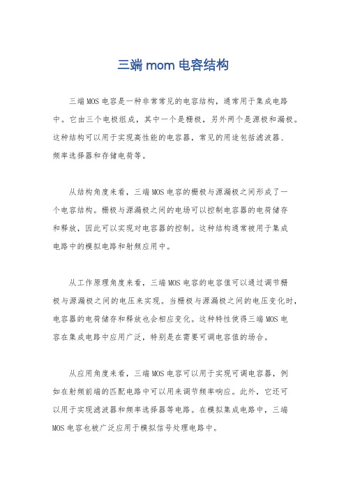
三端 mom电容结构
三端MOS电容是一种非常常见的电容结构,通常用于集成电路中。
它由三个电极组成,其中一个是栅极,另外两个是源极和漏极。
这种结构可以用于实现高性能的电容器,常见的用途包括滤波器、
频率选择器和存储电荷等。
从结构角度来看,三端MOS电容的栅极与源漏极之间形成了一
个电容结构。
栅极与源漏极之间的电场可以控制电容器的电荷储存
和释放,因此可以实现对电容器的控制。
这种结构通常被用于集成
电路中的模拟电路和射频应用中。
从工作原理角度来看,三端MOS电容的电容值可以通过调节栅
极与源漏极之间的电压来实现。
当栅极与源漏极之间的电压变化时,电容器的电荷储存和释放也会相应变化。
这种特性使得三端MOS电
容在集成电路中应用广泛,特别是在需要可调电容值的场合。
从应用角度来看,三端MOS电容可以用于实现可调电容器,例
如在射频前端的匹配电路中可以用来调节频率响应。
此外,它还可
以用于实现滤波器和频率选择器等电路。
在模拟集成电路中,三端MOS电容也被广泛应用于模拟信号处理电路中。
总的来说,三端MOS电容结构具有灵活可调的特点,可以在集成电路中实现多种功能,是集成电路设计中常用的元件之一。
调幅调频收音机的组装与调试实训报告
AM/FM收音机的安装与调试实训报告一、实训目的:1、学习收音机的调试与装配。
2、提高读整机电路图及电路板图的能力。
3、掌握收音机生产工艺流程,提高焊接工艺水平。
二、实训容:1、收音机电路原理分析。
2、掌握印制电路板的组装及焊接工艺。
3、进行AM、FM中频及统调覆盖的调试及整机测试。
4、故障判断及排除。
三、实训基本要求:1、会检测元器件并判别其质量。
2、独立完成各测试点的测量与整机安装。
3、会排除在调试与装配过程中可能出现的问题与故障。
四、实训步骤(一)对照元件清单表清点元件(二)元件的插接与焊接(三)收音机的整机调试1、调幅部分的调整①中频放大电路的调整——调AM中周➢调整时,整机置中波AM收音位置➢将音量电位器置于最大位置,将收音机调谐到无电台广播又无其它干扰的地方(或者将可调电容调到最大,即接收低频端)。
➢使高频信号发生器输出载频为465kHz,调制信号频率为1000Hz,调制度为30%的调幅信号接入IC的“10”脚。
➢用无感螺丝刀微微旋转中频变压器(黑色中周)的磁帽向上或向下调整,使示波器显示的波形幅度最大无失真。
在调整中频变压器时也可以用喇叭监听,当喇叭里能听到1000Hz的音频信号,且声音最大,音色纯正,此时可认为中频变压器调整到最佳状态。
②、调整接收围(频率覆盖)——调AM的电感和电容➢调整时,整机置中波AM收音位置。
➢将音量电位器置于最大位置。
低端频率调整:➢将可变电容器(调谐双联)旋到容量最大处,即机壳指针对准频率刻度的最低频端。
➢使高频信号发生器输出载频为515kHz,调制信号频率为1000Hz,调制度为30%的高频调幅信号接入IC的“l0”脚。
➢用无感螺丝刀调整中波振荡线圈的磁芯(红色中周),以改变线圈的电感量,使示波器出现1000Hz波形,并使波形最大。
或直接鉴听收音机的声音,使收音机发出的声音最响最清晰。
高端频率调整:➢将整机的可变电容器置容量最小处,这时机壳指针应对准频率刻度的最高频端。
- 1、下载文档前请自行甄别文档内容的完整性,平台不提供额外的编辑、内容补充、找答案等附加服务。
- 2、"仅部分预览"的文档,不可在线预览部分如存在完整性等问题,可反馈申请退款(可完整预览的文档不适用该条件!)。
- 3、如文档侵犯您的权益,请联系客服反馈,我们会尽快为您处理(人工客服工作时间:9:00-18:30)。
swsx vusy vuvs vwswvwvu!" 7 4# $8 %8 $4! 884%48 7&$345365)*+,-./+01,2,1*),3-)4564789:;58588<=>?@:98>?:AB *C +;589);5=>?B DC 14789:;58588<=>?E=986:=4>?E=986:=4>?E =986:=4>!" 7 4# $8 %8 $4! 884%48 7&$gg54>8>:@54>8>:@+986;G:=4>@a49:A8G@84a?8>89;<p Z11!" 7 4# $8 %8 $4! 884%48 7&$%8%8!" 7 4# $8 %8 $4! 884%48 7&$|6!" 7 4# $8 %8 $4! 884%48 7&$!" 7 4# $8 %8 $4! 884%48 7&$/:;?8@+986;G:=4>@)86A>=6;<64>@=E89;:=4>@VM /4<E89=>?PMX A8>:44J G6A A;<4?8>;:8E @GD@:;>68B 1A<49=>8l8:6C64>:8>:=@G@8E :4;6:=7;:8:A8a <G_l49A=?A<I ;6=E=6a <G_=@G@8El;>8_68@@=78;J 4G>:4a 98@=EG8;a :89@4<E89=>?J ;I <8;E :464994@=4>4a:A8:89J =>;<8<86:94E8@49E8?9;E;:=4>4a=>@G<;:=4>98@=@:;>684>:A8@G9a ;684a:A86;5;6=:49@M QM 2<G_=@G@8E :4=>698;@8@4<E89;D=<=:I =>a <4b @4<E89=>?lDG:=a:44J G6Aa <G_=@;55<=8El;<;9?8;J 4G>:4aa <G_?;@J ;I D88J =::8E ;>E J ;I E8:9=J 8>:;<<I ;a a 86:@4<E89;D=<=:I M)4J =>=J =^8:A8;J 4G>:4aa <G_;55<=8El =:=@9864J J 8>E8E :4G@8;a <G_U DGDD<=>?@I@:8J M[M /=>68:A898@=EG84ab ;:89U @4<GD<8a <G_=@8;@=<I E=@@4<78E DI b ;:8964>:8>:=>:A8;=9l:A898@=EG84>:A8@G9a ;684a6;5;6=:49@=>A=?A AGJ =E=:I 64>E=:=4>@J ;I 6;G@8;E8?9;E;:=4>4a=>@G<;:=4>98@=@:;>68;>E :A898a 498;a a 86::A898<=;D=<=:I 4a:A864J 54>8>:@M)A86<8;>=>?J 8:A4E@;>E :A86;5;D=<=:I 4a:A8J ;6A=>8@G@8E @A4G<E ;<@4D864>@=E898E 6;98a G<<I b A8>@8<86:=>?b ;:89U @4<GD<8a <G_M +98A8;:=>?b A8>@4<E89=>?Y 8;:=>?k+98A8;::A86A=5@;:POO:4P[O POO D8a 498@4<E89=>?M144<=>?k)A8:8J 589;:G98E=a a 898>68D8:b 88>:A864J 54>8>:@;>E 6<8;>=>?59468@@@A4G<E >4:D8?98;:89:A;>POO M189;J =66A=56;5;6=:49@;98@G@685:=D<8:4:A89J ;<@A46H b A8>8_54@8E :49;5=E 4964>68>:9;:8E A8;:=>?499;5=E 644<=>?l)A898a 498l:A8@4<E89=>?59468@@J G@:D864>EG6:8E b =:A ?98;:6;98@4;@:459878>:J ;<a G>6:=4>4a:A864J 54>8>:@EG8:48_68@@=78:A89J ;<@A46HM¡¢£¡¢£¡¢£¡¢£¡¢£¡¢£¤¥¤¦¤§¤¨¤¨¤©¤ª¤¢©¨¤¥©¨©¤««««««««««««««««««2222«2222T 2222««««¬ «¬ «¬ «¬«¬ «¬ «¬ «¬ «¬m864>J J 8>E8E /4<E89=>?p 8:A4E®¯°±²³´µ¶±·¸®°±¹¯®º®¯±²³´µ¬¬»¼±®¯°±²³´µ³½±¾±¶¿±²»·À²± »·±°£®¯·»µ±Á»¿»Â³·»´Â±®¯°±²³´µÁ¸»²»Â·±²³Ã·³ÂÃı·¸®°35!" 7 4# $8 %8 $4! 884%48 7&$3!" 7 4# $8 %8 $4! 884%48 7&$35%86%86h Í!" 7 4# $8 %8 $4! 884%48 7&$Stages Precautions Technical considerations8.Storage Condition s Storage1.To maintain the solderability of terminalelectrodes and to keep the packagingmaterial in good condition,care must betaken to control temperature and humidityin the storage area.Humidity shouldespecially be kept as low as possible.Recommended conditionsTemperature040Humidity Below70%RHThe room temperature must below40.Even under ideal storage conditions capacitor electrode solderability decreased as time passes,so ceramic chip capacitors should be used within6months from the time of delivery.The packaging material should be kept where nochlorine or sulfur exist in the air.2.The capacitance value of high dielectric constant capacitors(type2&3)will gradually decrease with thePassage of time,so this should be taken into consideration in the circuit design.If such a capacitance reduction occurs,a heat treatment of150for1hour will return the capacitance to its initial level.1.If the parts are stored in a high temperatureand humidity environment,problems such asreduced solderability caused by oxidation ofterminal electrodes and deterioration oftaping/packaging materials may take place.Forthis reason,components should be used within6months from the rime of delivery.If exceedingthe above period,please check solderabilitybefore using the capacitors.6.Post cleaning Processes With some type of resins a decomposition gas or chemical reaction vapor may remain inside the resin during the hardening period or even while left under normal storage conditionswill result in the deterioration of thecapacitor s ps hs o。