Noise floor in ADC testing
噪声系数的计算及测量方法
噪声系数的计算及测量方法(一)时间:2012-10-25 14:32:49 来源:作者:噪声系数(NF)是RF系统设计师常用的一个参数,它用于表征RF放大器、混频器等器件的噪声,并且被广泛用作无线电接收机设计的一个工具。
许多优秀的通信和接收机设计教材都对噪声系数进行了详细的说明.现在,RF应用中会用到许多宽带运算放大器和ADC,这些器件的噪声系数因而变得重要起来。
讨论了确定运算放大器噪声系数的适用方法。
我们不仅必须知道运算放大器的电压和电流噪声,而且应当知道确切的电路条件:闭环增益、增益设置电阻值、源电阻、带宽等。
计算ADC的噪声系数则更具挑战性,大家很快就会明白此言不虚。
公式表示为:噪声系数NF=输入端信噪比/输出端信噪比,单位常用“dB”。
该系数并不是越大越好,它的值越大,说明在传输过程中掺入的噪声也就越大,反应了器件或者信道特性的不理想。
在放大器的噪声系数比较低的情况下,通常放大器的噪声系数用噪声温度(T)来表示。
噪声系数与噪声温度的关系为:T=(NF-1)T0 或NF=T/T0+1 其中:T0-绝对温度(290K)噪声系数计算方法研究噪声的目的在于如何减少它对信号的影响。
因此,离开信号谈噪声是无意义的。
从噪声对信号影响的效果看,不在于噪声电平绝对值的大小,而在于信号功率与噪声功率的相对值,即信噪比,记为S/N(信号功率与噪声功率比)。
即便噪声电平绝对值很高,但只要信噪比达到一定要求,噪声影响就可以忽略。
否则即便噪声绝对电平低,由于信号电平更低,即信噪比低于1,则信号仍然会淹没在噪声中而无法辨别。
因此信噪比是描述信号抗噪声质量的一个物理量。
1 噪声系数的定义要描述放大系统的固有噪声的大小,就要用噪声系数,其定义为设Pi为信号源的输入信号功率,Pni为信号源内阻RS产生的噪声功率,Po和Pno 分别为信号和信号源内阻在负载上所产生的输出功率和输出噪声功率,Pna表示线性电路内部附加噪声功率在输出端的输出。
洁净室测试标准程序
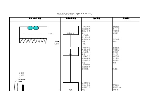
测试方法之图解 测试流程图解 测试程序 注意要点
FFU Ceiling 天花板
准备工作
1. 准备好测试所需要的图纸,噪音仪, 要特别检查一下所有需要的文件是 记录表格,及其他所需要的测试材 否已准备就续。 料。 2. 确保所有的设备均在运行之中,并且 要确保没有其他活动在进行,因 确认没有任何有可能产生噪音进而会 而此项测试一般建议在假日或夜 影响到测试结果的动作在发生。 间进行。
测试
FFL+1000mm
记录测试结果
地板 Grating Floor
5. 记录下所有的测试数据,并确认对每 一频率的噪音均进行了测试。如果某 一数据在测试过程中,受到其它噪音 的干扰,需特别注明。
确认
噪音仪ter
设置
3. 调整好噪音仪,保证对其进行正确的 将噪音仪调整至“A”级水平, 操作,同时还需确保噪音仪在测试前 and "All Pass",并检查所用的电 已校准过。 池是否是新的。 4. 依据图纸上业主认可的位置开始进行 测试, 并确认没有其它噪音会干扰到 测试的进行。具体测试方法请参照旁 边测试方法之图解中所示。 在所有的空调系统设备运行之前, 需预先对测试区域的背景噪音进行 测试,并特别记录下任何其它不属 需测试系统内噪音的数据。
噪声测试实验步骤
噪声测试实验步骤噪声测试实验步骤1、确定所依据的标准文件1)国标、以及国际性标准。
2)客户的要求。
噪声测试实验步骤2、明确测量环境1)自由声场------全消声室2)半自由声场------半消声室噪声测试实验步骤3、选择所要使用的测量仪器1)根据标准要求来选择。
2)根据测量仪器本身的性质(不同量程、不同测试环境,自由场/压力场)来选择。
3)对所选的测量仪器进行检查(校准有效期、或用声校准器现场校准),以确保测量数据受控、可靠。
噪声测试实验步骤4、准备测量1)根据被测样品及测试所依据的标准文件摆放被测样品,安装测试传声器。
2)记录试验条件(试验时间、试验地点、试验环境、环境温湿度、标准依据、被测件工作状态、传声器安装位置、测试人员等)。
3)在测试开始前,测量试验环境的本底噪声,并做记录。
噪声测试实验步骤5、测试依据标准或测试需求进行测试仪器的设置,并进行测试。
噪声测试实验步骤6、数据记录按照测试标准要求及测试需求记录原始记录,需要进行数据处理的试验,在记录原始记录时一定要把所有原始实测数据记录下来,不可只记录二次处理后的数据,不记录最原始数据。
噪声测试实验步骤7、数据处理需进行原始数据处理的试验,在原始数据记录完后按照所依据标准进行数据处理,并将处理过程一并体现在原始记录中。
噪声测试实验步骤8、试验结束试验结束后,对噪声测量系统进行二次校准确认,以确保测试数据准确可靠。
噪声测试实验步骤9、常见问题对一类样品的测试,要确保测试条件的一致性和可复现性。
包括:1)测试仪器的一致性2)测试仪器设置的一致性3)测试环境的一致性4)测试位置的一致性5)被测样品工作状态的一致性。
ADC测试方案

4. SINAD
SINAD=20log10(RMS[harmonic]+RMS[signal]/RMS[signal])
5. 最大有效位数:ENOB ENOB=(SNR-1.76)/6.02
动态参数matlab计算结果
采样时钟: FS=184MSPS 待测信号: FIN=170MHz
ADC测试
ADC产品简单介绍
使用场合:
无线基站、直放站
CT 、核磁共振 雷达、军事 仪器仪表等
市场上主流的ADC产品基本上是TI和ADI的,国内也有一 些设计公司和研究所在做,目前国内的技术水平如下:
8位ADC采样率超过1Gsps
12位采样率超过300Msps
16位采样率超过150Msps
量产测试
装备有测ADC的板卡的ATE有
1. Teradye J750 模拟信号低于2MHz 2. Teradye Ultra Flex 模拟信号1GHz
3. Advantest 93K 模拟信号1GHz
4. Credence D10
ATE模拟板卡的功能结构图
任意信号发生器
(AWG)
DUT
Digitizer
用这个方法。这种方法需要采集很多样本,样本越多,测得数据越精确。
静态参数matlab计算结果
采样时钟: FS=184MSPS 待测信号: FIN=1.9MHz 样本数据:4百万个
动态技术参数
1. 信噪比:SNR SNR=20log10(RMS[signal]/RMS[Noise]) 2. 最大杂散:SFDR SFDR=20log10(Max [spur]/RMS[signal]) 3. 谐波抑制比:THD
adc评估板

adc评估板ADC是模数转换器(Analog-to-Digital Converter)的简称,它的作用是将模拟信号转换为数字信号。
ADC评估板则是用来评估ADC性能的工具,可以对ADC进行测试、调试和性能评价。
以下是对ADC评估板的评估。
首先,ADC评估板的硬件设计需要考虑其性能指标。
首先是分辨率,即ADC可以转换的模拟信号的精度。
通常用位数表示,比如12位、16位等。
分辨率越高,转换精度越高。
此外,还要考虑采样率,即ADC转换的频率,通常用每秒转换次数(SPS)表示。
采样率越高,ADC能够转换的信号频率范围越宽。
还要考虑功耗、信噪比、线性度等硬件指标。
其次,ADC评估板的软件设计也是评估的重要内容。
首先是驱动程序的设计,ADC评估板需要能够与主控板进行通信,驱动程序需实现数据的读取和控制。
其次是界面程序的设计,用于显示和分析ADC转换的数据。
界面程序应具有友好的用户界面,支持实时显示和存储数据,方便用户对ADC性能进行分析和评价。
还要考虑软件的稳定性和易用性。
接着,进行ADC评估时,需要进行一系列测试。
首先是静态测试,即对ADC的基本性能进行测试,包括测量ADC的分辨率、采样率、信噪比、线性度等,以及对不同输入信号进行转换,并对转换结果进行验证。
然后是动态测试,即测试ADC在不同输入信号条件下的动态性能,比如信号频率、幅值等。
这一系列测试可以帮助用户了解ADC的性能,并选择适合自己应用的ADC。
最后,还要对ADC评估板进行性能评价。
评估板的性能直接影响到对ADC的评估准确性,所以评估板的硬件设计和软件设计都需要考虑。
评估板的性能包括了稳定性、准确性、可靠性等。
在评估过程中,用户可以通过与规格书的对比来评估评估板的性能是否符合设计要求。
综上所述,ADC评估板是对ADC性能进行评估的重要工具。
评估板的硬件设计和软件设计都需要考虑,测试和评价结果也是评估板的重要部分。
通过对ADC评估板的评估,可以更好地了解和选择适合自己应用的ADC,提高系统性能和稳定性。
ADC Testing
–
Code 1
Code 2
Input Voltage Probability
Area 1 = Probability for Code 1
D V
Area 2 = Probability for Code 2
Input Voltage (DC Plus Noise)
ADC Testing Versus DAC Testing
Code 1
Code 2
Input Voltage Probability
50% Probability for Code 1
50% Probability for Code 2
Input Voltage (DC Plus Noise)
ADC Testing Versus DAC Testing
ADC Decision Levels Code 1
Gaussian Noise pdf
Code 2
Input Voltage Probability
Average Voltage (DC Input)
Input Voltage (DC Plus Noise)
ADC Testing Versus DAC Testing
ADC Testing Versus DAC Testing
–
Statistical Behavior of ADCs
–
To understand the statistical nature of ADCs, we have to model the ADC as a combination of a perfect ADC and a noise source with no DC offset.
MT-005噪声功率比(NPR)—拥有65年历史的电话系统参数在现代无线应用中重获新生
e(x)
q = 1 LSB
CLIPPING REGION
e(x) = x – VO x
CLIPPING REGION
–VO
0
+VO
e(x) = ERROR (INPUT – OUTPUT)
图3:理想ADC误差波形
Page 4 of 12
MT-005
量化噪声组分(表示为实际量化噪声电压的平方,结果得到噪声功率)为(见参考文献2): 等式 2 其中,q为最低有效位(LSB)的权重。需要注意的是,这是在整个奈奎斯特带宽直流至fs/2的 范围内测得的量化噪声功率。如果信号带宽减小,减小的带宽中的噪声会按比例减少,必 须增加一个校正因数(本文后面将讨论这一点)。 继续推导,可知,q = 2VO/2n。因此,由等式2得出:
Page 2 of 12
MT-005
1966年,CCITT/CCIR把针对FDM系统提出的系统NPR建议正式化,以便测量频分多路 (FDM)通信链路的传输特性(见参考文献4)。 在含有一个ADC的数字系统中,当施用的是低电平输入噪声时,陷波内的噪声主要是量化 噪声。然而,对于极低幅度信号(低于1 LSB峰峰值),结果产生的噪声返回ADC等效输入噪 声。对于使用该ADC的多个LSB的信号,NPR曲线呈线性,主要是量化噪声。随着噪声电 平的提高,噪声电平与NPR之间存在一一对应关系。然而,在某个电平下,ADC的硬限幅 行为导致的“削波”噪声将开始占据主导地位。ADC硬限幅“削波”噪声与模拟FDM的软限幅 “过载”噪声有所不同,在削波区产生“较陡”的向下斜坡。 针对数字系统的理论NPR值 多年以来,有几篇论文探讨了针对一种理想n位ADC的理论NPR值(如参考文献5、6、7)。 其中,参考文献6是最完善的,同时展示了均匀分布噪声和高斯噪声的推导过程。然而, 高斯噪声与NPR测试的相关性更高。虽然推导过程并不难,但确实涉及一些偏积分。由于 “削波”噪声组分并无闭式解,因此,在实际计算过程中,必须使用数值法来计算理论NPR 值。 10、 12、 14和 16位 ADC的 理 论 曲 线 如 图 2所 示 。 了 解 项 V O 、 σ、 k和 均 方 根 加 载 电 平 (–20log10k)的定义对于避免混淆是十分重要的。
理解模数转换器的噪声_ENOB和有效分辨率
ADC的主要趋势之一是分辨率越来越高。
这一趋势影响各种应用,包括工厂自动化、温度检测和数据采集。
对更高分辨率的需求正促使设计者从传统的12位逐次逼近寄存器(SAR)ADC转至分辨率高达24位的Δ-ΣADC。
所有的ADC都会具有一定的噪声,这包括输入参考噪声(ADC固有噪声)和量化噪声(ADC转换时产生的噪声)。
诸如噪声、ENOB(有效位数)、有效分辨率和无噪声分辨率等指标在很大程度上定义了ADC的实际精度。
所以,理解与噪声相关的性能指标是从SAR 过渡至Δ-ΣADC最困难的方面之一。
由于当前对更高分辨率的迫切需求,设计者必须更好地理解ADC噪声、ENOB、有效分辨率,以及信噪比(SNR)。
本文的目的正基于此。
Δ-ΣADC的更高分辨率和价值在过去,12位SAR ADC通常足以满足各种信号和电压输入的测量。
如果应用中需要更为精细的测量,可在ADC之前增加增益级或可编程增益放大器(PGA)。
分辨率为16位时,设计者的选择仍然主要是SAR ADC,但也包括部分Δ-ΣADC。
然而,对于需要16位以上分辨率的设计,Δ-ΣADC则更为普遍。
SAR ADC目前受限于18位,而Δ-ΣADC则延伸至18、20和24位。
Δ-ΣADC还有其它优势。
其价格在过去10年中已大幅下降,使用越来越简单,已被广泛接受。
有效分辨率有效分辨率由下式定义(以位为单位):有效分辨率= log2 [满幅输入电压范围/ADC RMS噪声]或更为简单:有效分辨率= log2 [VIN/VRMS NOISE]切勿将有效分辨率与ENOB相混淆,尽管两者听起来非常类似。
测量ENOB的最常见方法是对ADC的正弦波输入进行FFT分析。
IEEE(r)标准1057将ENOB定义为:ENOB = log2 [满幅输入电压范围/(ADC RMS噪声×√12)]SINAD定义为信噪比加失真比。
SINAD和ENOB用于衡量ADC的动态性能。
所以:SINAD = [RMS输入电压/RMS噪声电压]式中,RMS噪声= 1/M[eq1。
接收机噪声系数测试方法
接收机噪声系数测试方法接收机的噪声系数是衡量其信号接收能力的重要指标之一、噪声系数表示接收机输入信号与输出信号之间的信噪比损失。
噪声系数越小,接收机的信噪比损失越小,其性能越好。
为了保证接收机的正常工作,需要定期对其噪声系数进行测试。
接收机的噪声系数测试可通过外参考源法或内参考源法来进行。
一、外参考源法:使用外部噪声源作为参考源来测试接收机的噪声系数。
一般情况下,可以使用陶瓷电阻、热电偶和大气热噪声等作为外参考源。
1.陶瓷电阻法:陶瓷电阻法是一种常用的测试方法,其原理是使用陶瓷电阻作为产生噪声的源,通过测量输出信号的功率和输入信号的功率来计算噪声系数。
测试步骤如下:1)将陶瓷电阻与接收机的输入端相连接;2)打开接收机,通过调节陶瓷电阻的阻值,使得接收机输出的信号功率达到最大;3)测量陶瓷电阻的阻值、接收机输出信号的功率和输入信号的功率;4)根据功率的大小计算噪声系数。
2.热电偶法:热电偶法是利用热电偶作为外参考源,通过测量输出信号的功率和热电偶的温度来计算噪声系数。
测试步骤如下:1)将热电偶与接收机的输入端相连接;2)打开接收机,通过调节热电偶的温度,使得接收机输出的信号功率达到最大;3)测量热电偶的温度、接收机输出信号的功率和输入信号的功率;4)根据功率和温度的大小计算噪声系数。
3.大气热噪声法:大气热噪声法是利用地球大气的热噪声作为外参考源,通过测量输出信号的功率和大气热噪声的温度来计算噪声系数。
测试步骤如下:1)将天线与接收机的输入端相连接;2)选取一个没有无线电源干扰的地点进行测量;3)打开接收机,测量接收机输出信号的功率和大气热噪声的温度;4)根据功率和温度的大小计算噪声系数。
使用外参考源法进行噪声系数测试的优点是测试结果准确,可靠性高。
但同时需要提前准备好相应的外参考源。
二、内参考源法:使用接收机自身内部的参考源来进行噪声系数测试,常用的内参考源包括内部噪声源、参考输入端口和本地参考振荡器等。
集成电路测试工作流程英语小作文
集成电路测试工作流程英语小作文英文回答:Integrated circuit (IC) testing is a crucial step in ensuring the quality and reliability of electronic devices. It involves a systematic process to verify thefunctionality and performance of ICs before they are integrated into final products. Here's a breakdown of the typical workflow involved in IC testing:1. Test Planning and Strategy: Before testing begins,it's essential to develop a comprehensive test plan outlining the objectives, methodologies, and resources required for testing. This phase involves understanding the specifications of the ICs and defining the test coverage criteria. For example, if I'm testing a microcontroller,I'll need to consider factors like input/output functionality, clock speed, and power consumption.2. Test Development: Once the test plan is in place,the next step is to develop test programs or patterns that will be used to stimulate the IC and capture its responses. This involves writing code or using specialized software tools to generate test vectors. These vectors represent different input stimuli applied to the IC to evaluate its behavior under various conditions. For instance, if I'm testing a memory chip, I'll create test patterns to read and write data to different memory locations to check for any defects or inconsistencies.3. Test Execution: With test programs ready, it's time to execute them on the target ICs. This phase involves connecting the ICs to test equipment such as automated test equipment (ATE) or specific test fixtures. The ICs are subjected to the test patterns, and their responses are analyzed to determine whether they meet the expected specifications. During this stage, it's essential to monitor parameters like voltage, frequency, and temperature to ensure accurate testing. For example, if I'm testing a digital signal processor (DSP), I'll verify its computational accuracy by running mathematical algorithms and comparing the results against expected values.4. Data Analysis and Debugging: After completing the tests, the data collected needs to be analyzed to identify any deviations or failures. This involves comparing the actual test results with the expected outcomes specified in the test plan. If discrepancies are found, debugging techniques are employed to pinpoint the root cause of the issues. For instance, if I encounter failures in the output of an analog-to-digital converter (ADC), I'll investigate factors like noise, linearity, or calibration errors that could affect its performance.5. Reporting and Documentation: Finally, the results of the testing process are documented in detailed reports. These reports include summaries of the tests conducted, the outcomes obtained, any anomalies detected, and recommendations for further actions. Clear documentation is crucial for traceability and quality assurance purposes. Additionally, lessons learned from the testing process are recorded to improve future testing strategies and methodologies.In conclusion, the workflow for IC testing involves careful planning, meticulous execution, and thorough analysis to ensure the reliability and functionality of integrated circuits. By following a systematic approach and leveraging advanced testing techniques, manufacturers can deliver high-quality ICs that meet the demands of modern electronic devices.中文回答:集成电路(Integrated Circuit,IC)测试是确保电子设备质量和可靠性的关键步骤。
- 1、下载文档前请自行甄别文档内容的完整性,平台不提供额外的编辑、内容补充、找答案等附加服务。
- 2、"仅部分预览"的文档,不可在线预览部分如存在完整性等问题,可反馈申请退款(可完整预览的文档不适用该条件!)。
- 3、如文档侵犯您的权益,请联系客服反馈,我们会尽快为您处理(人工客服工作时间:9:00-18:30)。
Noise floor in ADC testingDavid Slepi čkaCzech Technical University in Prague, Faculty of Electrical Engineering, Dept. of MeasurementTechnická 2, CZ-16627 Prague 6, Czech RepublicPhone: ++ 420 2 2435 2058, Fax: ++ 420 2 3333 9929, E-mail: slepicd@fel.cvut.czAbstract - The main goal of this paper is to introduce several definitions of noise floor and to show their application in ADC testing with regard to straightforward reading of some basic ADC parameters. The definitions and algorithms can be used for ADC standardization.I. IntroductionNoise floor is a frequency spectrum parameter that is widely used in ADC testing although it has not been properly defined and described by a formula in any ADC standards yet. IEEE Std 1057-1994 does not mention the noise floor but it generally uses noise or noise level that is not defined. IEEE Std 1241-2000 provides a formula for noise floor computation depending on the number of ADC bits; consequently, such noise floor corresponds to that of the ideal ADC and not to the reality. In the last version of DYNAD (version 3.3, Sept. 2000), the definition of the noise floor is the most precise. Harmonic components, gain and offset errors are not considered there when determining the noise floor and a formula for noise floor computation is also provided. Unfortunately, only white noise is used in this standard and spurious components are not considered there.The noise floor is commonly understood as the average (sometimes also maximal) power of random noise (i.e. the noise that is freed of any harmonic, spurious and DC components) in frequency spectrum. It implies that the noise floor determines the detection power level under which no weak signals can be discovered. It also determines power uncertainty of evaluation of any spectral component due to noise. So, the noise floor is important information in frequency domain. Once estimated, it can be used e.g. for the detection of strong spectral components.II. Noise floorsWhen noise is the product of quantization, the noise floor can be derived using an ADC parameter, SNR —signal to noise ratio. If the ADC input signal is a sine-wave signal that spans the full-scale range of the converter, the SNR can be expressed using the well-known formula76.102.6)dBfs (+=N SNR (1)where N is the number of ADC bits. As the noise is assumed to be white, the value of the SNR determines the noise floor level. The SNR is often computed for the signal that does not fully cover the ADC full-scale range. In this case, the noise floor, NF , has to be corrected for the signal to full-scale ratioRMSRMS scale full signal SNR SNR NF log 20)dBc ()dBfs ()dBfs (+−=−=. (2) When the signal of interest occupies a smaller bandwidth, BW , which is less than the Nyquist bandwidth, a digital filter can filter out the noise outside the bandwidth BW . In this case, the noise floor is increased by the factor called processing gainBW f SNR NF s 2log 10)dBfs ()dBfs (10−−= (3)where f s equals the sampling frequency. Typical example of a digital filter is the DFT algorithm. The DFT acts as a bank of digital filters each of bandwidth f s /M where M is the DFT length. So, the noise floor in the DFT spectrum is done by2log 10)dBfs ()dBfs (10M SNR NF −−=. (4)Moreover, if a non-rectangular window is applied to the signal, this formula has to be corrected by the equivalent noise bandwidth, ENBW , of the windowENBWM SNR NF 2log 10)dBfs ()dBfs (10−−=. Note that windowing decreases the leakage effect but it also decreases frequency resolution and it worsens the noise floor (ENBW ≥ 1). Thus, special care should be taken when choosing the window.Short analysis made above is the basis of the most definitions of the noise floors in ADC testing. In the following subsections, several various noise floors are proposed. All noise floor definitions are summarized in appendix at the end of this paper.A. Ideal noise floorAs mentioned above, the definition of the noise floor according to the IEEE Std 1241-2000 corresponds to the noise floor of an ideal N-bit ADCENBW M N NF ideal 2log 1076.102.6)dBfs (10−−−=. (6)Although this value is practically unreachable, if plotted in the amplitude frequency spectrum it shows the limitation of the used ADC (see Fig. 3). The difference between the actual and ideal noise floors also corresponds to the ratio of the actual and ideal noise. This ratio determines how many ADC bits are lost due to random noise (common noise floor) or noise plus distortion (effective noise floor). This information can be directly estimated from the frequency spectrum what is not commonly possible.B. Thermal noise floorHowever precise the ADC is, the noise floor is physically limited by the noise generated by the thermal agitation of the electrons. Such noise is called thermal, Johnson or Nyquist and its power can be computed asBW T K P thermal ⋅⋅=)W ( (7)where K is Boltzmann's constant (K =1.381·10–23 W/Hz/K) and T equals the absolute temperature in kelvins. The noise floor determined by the thermal noise at room temperature expressed in dBm units can be estimated asBW NF thermal 10log 10174)dBm (+−=. (8)E.g. the thermal noise floor equals –174 dBm in 1 Hz bandwidth and –134 dBm in 10 kHz bandwidth.dBm units reflect the fact that the thermal noise floor is an absolute number unlike other noise floors that are expressed relatively to the ADC full-scale range. If ADC full-scale voltage, U fs , and input resistance, R , are known, the thermal noise floor can be expressed in dBfs units asR U BW T K NF RMS fs thermal 2,1010log 10log 10)dBfs (−⋅⋅=. (9)In ADC testing, this conversion is needed for displaying the thermal noise floor in amplitude frequency spectrum of the sampled signal that is commonly plotted in dBfs units there. In case of sampled signal, the thermal noise bandwidth, BW , equals the Nyquist frequency, f s /2. If the amplitude frequency spectrum is computed by means of the DFT algorithm, the processing gain has to be added, tooENBW f T K R U M NF s fs RMS thermal ⋅⋅⋅⋅⋅−=2,10log 10)dBfs (. (10)The difference between the thermal and (dynamic) common noise floors equals the noise figure. A simplified diagram of several noise floors is shown in Fig. 1.C. Effective noise floorWhen the number of ADC bits in (6) is replaced by the effective number of ADC bits, the effective noise floor is obtainedENBW M SINAD ENBW M N NF ef ef 2log 10)dBfs (2log 1076.102.6)dBfs (1010−−=−−−=. (11)This noise floor corresponds to overall ADC performance and if plotted in the amplitude frequency spectrum it offers a quick comparison with the common noise floor. If the effective noise floor is noticeably above the common noise floor, the overall ADC performance is considerably limited also by spurious and/or harmonic components.D. Common noise floorIf the noise in amplitude frequency spectrum is freed of harmonic and spurious components, the average power of this noise corresponds to the common noise floor. In ADC testing, a parameter called the signal to non-harmonic ratio, SNHR , is frequently used. Accordingly, the SNHSR parameter can represent the signal to non-harmonic non-spurious ratio. Using this parameter, the common noise floor is given byENBW M SNHSR NF 2log 10)dBfs ()dBfs (10−−=. (12)The common noise floor represents the average random noise power in frequency spectrum. The level of the common noise floor can be advantageously used for further data processing e.g. for distinguishing strong and weak components in the frequency domain. Unfortunately, strong spectral components are needed to be known and their power subtracted from random noise power before the computation of the common noise floor.E. Dynamic (common) noise floorThe computation of the common noise floor by formula (12) assumes white noise. If the noise is colored, the noise level computed by this formula does not follow frequency dependence of random noise. Thus, it is advantageous to compute the common noise floor dynamically in dependence on frequency.The approximation by a simple polynomial is mostly sufficient. As the noise in dependence on frequency usually varies in logarithmic scale, the approximation is more precise when also done in logarithmic scale. Note that such approximation is biased due to the logarithm. If the variance of amplitude frequency spectrum is decreased by averaging (Welch method), the bias is essentially reduced.III. Recognition of strong spectral componentsAfter the dynamic noise floor is determined, strong spectral components can be recognized as the components bigger than a certain threshold above the dynamic noise floor. As already mentioned, the problem is that strong spectral components are needed to be known for the determination of the dynamic noise floor.Fig. 1. Simplified diagram of noise floor levelsnoise floor iteratively (see Fig. 2). In the firstcomponents is estimated. The dynamic noisefloor is computed from the averaged powerrecognized using a specific threshold, then.These components are excluded from the amplitude frequency spectrum for the nextFortunately, no iteration is mostly necessaryand the number of iteration does not exceedusually dominates the power of spurious and harmonic components. applied even for windowed signals. If severalbandwidth, they can increase local dynamic floor can be decreased in next iteration(s); ifcomponents is close to random noise in this processed as random noise.The proposed noise floor definitions were applied on experimental data gained by acquisition by several different ADCs for pure sine-wave input signals. The acquired data were used for the computation of averaged power spectra (Welch method) from which amplitude frequency spectra were computed. Noise floors as well as the most important spectral parameters of the tested ADCs (SINAD , THD and SNHR ) were estimated and shown in amplitude frequency spectrum.Fig. 3a shows the computed amplitude frequency spectrum of an AD7793 evaluation board. The overall ADC performance expressed by the SINAD is obviously given by dominating ADC noise (plus spurious components) as SINAD ≅ SNHR . This fact can also be directly estimated from no significant difference of the effective and common noise floor levels displayed in amplitude frequency spectrum. The only distinction between these two ways of estimation is that unlike the SNHR , the common noise floor does not contain the power of spurious components; their power is usually negligible in practice, though.The dynamic noise floor was gained by the approximation of 9th order polynomial. The order of nine was found out to be the best choice in practice. Lower orders do not approximate local average a) AD7793 evaluation board (16 bits, f s =500 Hz, 64 kSa) b) PXI NI-5922 (24 bits, f s =10 MHz, 256 kSa)Fig. 3. ADC noise floors plotted in amplitude frequency spectrapower of noise well and higher orders react too quickly to any change in spectrum. Note good approximation of noise trend and significant difference of common and dynamic noise floors.Strong spectral components were found out in the frequency spectrum with the threshold of 8 dB from the dynamic noise floor. Weak harmonic components were signed by lighter color in the amplitude frequency spectrum. The optimal threshold level depends on random noise variance and the number of averages. In practice, the threshold in the range 6–10 dB is recommended.The level of the ideal noise floor shows that the actual ADC performance is much bellow its nominal resolution. Only at higher frequencies, the dynamic noise floor approaches the ideal noise floor due to strong ADC internal digital filtering. The thermal noise floor level indicates that the ideal noise floor is unreachable in this test configuration because of the thermal noise.Similar conclusions can be made in case of amplitude frequency spectrum of the PXI NI-5922 digitizer shown in Fig. 3b. The effective noise floor level is noticeably above common noise floor. It means that the overall ADC performance is considerably influenced also by harmonic distortion. The dynamic noise floor is relatively close to the thermal noise floor, especially at low frequencies; this indicates a good ADC noise performance. Huge gap between the ideal and dynamic noise floors implies that much lower number of nominal ADC bits would be sufficient for the same ADC performance.V. ConclusionIn this paper, several noise floors were characterized, defined and described by formulae. The usage of the noise floors was shown on practical ADC measurements and quick reading of some basic ADC parameters by means of noise floors was stressed. The application of the noise floor was shown on the detection of strong spectral components.References[1] IEEE Std. 1057-1994. “IEEE standard for digitising waveform recorders”. The Institute ofElectrical and Electronics Engineers, Inc., New York, 1994.[2] IEEE Std 1241-2000, “IEEE Standard for Terminology and Test Methods for Analog-to-DigitalConverters”, The Institute of Electrical and Electronics Engineers, Inc., New York, 2000.[3] DYNAD version 3.3, “Methods and draft standards for the DYNamic characterization and testingof Analogue to Digital converters,” European project DYNAD – SMT4-CT98-2214, Programme Standards, Measurements, and Testing, Sept. 2000.[4] W. Kester, “MT-001: Taking the Mystery out of the Infamous Formula, "SNR=6.02N + 1.76dB,"and Why You Should Care,” REV. 0, 10-03-2005, Analog Devices,/en/content/0,2886,761%255F795%255F88014,00.html.[5] “How Quantization and Thermal Noise Determine an ADC's Effective Noise Figure”, applicationnote 1197, Dallas Semiconductor, Sept. 2002.Appendix: Noise floor definitionsIdeal noise floorAverage power level of quantization noise of an ideal ADC in the frequency spectrum.Thermal noise floorAverage power level of the noise generated by the thermal agitation of the electrons over a given bandwidth in the frequency spectrum.Effective noise floorAverage power level of ADC noise, distortion and spurious components in the frequency spectrum. Common noise floorAverage power level of the ADC noise without spurious and harmonic components in the frequency spectrum.Dynamic (common) noise floorTrend of average power level of the ADC noise without spurious and harmonic components in the frequency spectrum.。