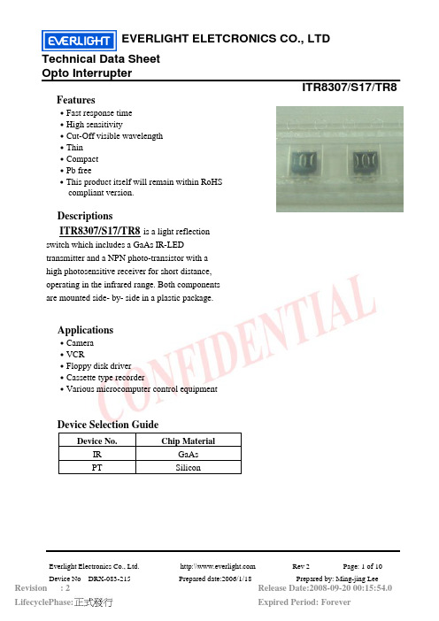
亿光 贴片反射式光耦 光电开关ITR8307-S17-TR8
el817工作原理
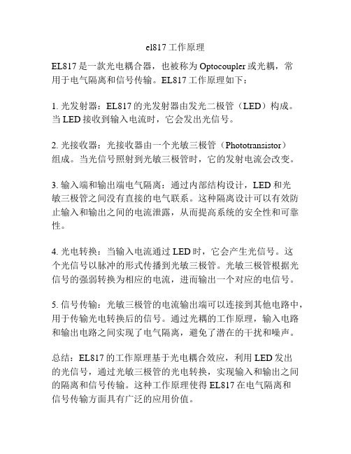
el817工作原理
EL817是一款光电耦合器,也被称为Optocoupler或光耦,常
用于电气隔离和信号传输。
EL817工作原理如下:
1. 光发射器:EL817的光发射器由发光二极管(LED)构成。
当LED接收到输入电流时,它会发出光信号。
2. 光接收器:光接收器由一个光敏三极管(Phototransistor)
组成。
当光信号照射到光敏三极管时,它的发射电流会改变。
3. 输入端和输出端电气隔离:通过内部结构设计,LED和光
敏三极管之间没有直接的电气联系。
这种隔离设计可以有效防止输入和输出之间的电流泄露,从而提高系统的安全性和可靠性。
4. 光电转换:当输入电流通过LED时,它会产生光信号。
这
个光信号以脉冲的形式传播到光敏三极管。
光敏三极管根据光信号的强弱转换为相应的电流,进而输出一个对应的电信号。
5. 信号传输:光敏三极管的电流输出端可以连接到其他电路中,用于传输光电转换后的信号。
通过光耦的工作原理,输入电路和输出电路之间实现了电气隔离,避免了潜在的干扰和噪声。
总结:EL817的工作原理基于光电耦合效应,利用LED发出
的光信号,通过光敏三极管的光电转换,实现输入和输出之间的隔离和信号传输。
这种工作原理使得EL817在电气隔离和
信号传输方面具有广泛的应用价值。
光电开关简介ppt课件可修改文字

光幕应用(续) 木材外形截面积检测
光幕应用(续)
光幕可检 测出带材在 卷曲过程中 的偏移,经 控制器和执 行机构使带 材向正确的 方向运动 (纠偏)。
纠偏
光幕应用(续)
光幕用于 自动收费系统的
车辆检测
超限超载车辆经过固定式称重台时, 计算机管理系统自动生成车牌号,轮轴 数.车货总重,车长,车速,车辆通过后 红外线收尾系统自动提示检测完毕.
反射式光电
直射型光电开关的发射器和接收器相对安放,轴线严格对准。 相应地,接收光电元件的输出信号经40kHz选频交流放大器及专用的解调芯片处理,可以有效地防止太阳光、日光灯的干扰,又可减
断续器 小发射LED的功耗。
反射镜使用偏光三角棱镜,能将发射器发出的光转变成偏振光反射回去,光接收器表面覆盖一层偏光透镜,只能接受反射镜反射回来 的偏振光。 被测物漫反射型光电开关原理 请写出转速与频率的关系式 光电断续器是较便宜、简单、可靠的光电器件。 它广泛应用于自动控制系统、生产流水线、机电一体化设备、办公设备和家用电器中。 漫反射型光电开关的应用 直射型光电开关的发射器和接收器相对安放,轴线严格对准。 当被检测物体位于发射器和接受器之间时,光线被阻断,接受器接受不到红外线而产生开关信号。 反射型光电开关分为两种情况: 被测物漫反射型(简称散射型)。 反射镜使用偏光三角棱镜,能将发射器发出的光转变成偏振光反射回去,光接收器表面覆盖一层偏光透镜,只能接受反射镜反射回来
光电断续器外形
两个柱形结构相对而立,每隔数十毫米安装一对发光二极管和光敏接收管,形成光幕,当有物体遮挡住光线时,传感器发出报警信号。 超限超载车辆经过固定式称重台时,计算机管理系统自动生成车牌号,轮轴数. 超限超载车辆经过固定式称重台时,计算机管理系统自动生成车牌号,轮轴数. 遮断式光电开关(计数) 光电开关在流 水线上的应用 一、光电开关的结构和分类 反射镜反射型光电开关集光发射器和光接受器于一体,与反射镜相对安装配合使用。 漫反射型光电开关的应用 光幕可检测出带材在卷曲过程中的偏移,经控制器和执行机构使带材向正确的方向运动(纠偏)。 被测物漫反射型(简称散射型)。 车货总重,车长,车速,车辆通过后红外线收尾系统自动提示检测完毕. 定区域式光电开关有一个非常确定的检测区域,不经过该区域的被测物体不会引起光电开关产生开关信号。 反射镜使用偏光三角棱镜,能将发射器发出的光转变成偏振光反射回去,光接收器表面覆盖一层偏光透镜,只能接受反射镜反射回来 的偏振光。 但在实际制作中,上下两路总存在干扰,很难提高测量精度。 对于漫反射式光电开关发出的光线需要被检测物表面将足够的光线反射回接收器,所以检测距离和被检测物体的表面反射率及粗糙程 度将决定接收器接收到光线强度,被检测物体的表面还应尽量垂直于光电开关的发射光线。 光电断续器可分为直射式(槽式)和反射型两种。 直射式光电开关由相互分离且相对安装的光发射器和光接受器组成。 红外LED的正向压降约为1. 超限超载车辆经过固定式称重台时,计算机管理系统自动生成车牌号,轮轴数. 光电断续器是较便宜、简单、可靠的光电器件。
夏普光耦选型手册
4脚 DIP
PC815XNNSZ0F*5, *6 复 合 光 晶 PC81510NSZ0X 体 管 5, 6 输 PC852XNNSZ0F* * 出 PC853XNNSZ0F*5, *6
*1 *2 *3 *4 *5 *6 *7 *8 *9
–
–
50
5.0
35
600
1
60
100
⅜ ⅜ ⅜
– ⅜ ⅜
–
10
页码 40 40 40 40 40 40 41 41 41 41 41 41 41 42 42 42 42 42 42 43 43
<OPIC 输出型>
封装类型 输出类型 特点 型号 (系列) PC400J00000F/PC456L0NIP0F/ PC410S0NIP0F /PC410L0NIP0F / PC4D10SNIP0F PC457S0NIP0F /PC457L0NIP0F 页码
PC714V0NSZXF PC724V0NSZXF
高绝缘电压 高绝缘电压, 大输入电流 高绝缘电压, 带基底端子 高绝缘电压, 高灵敏度 高绝缘电压, 高灵敏度, 高集电极发射极电压, 大功率
PC3HU7xYIP0B
PC3H2J00000F (小扁平型4脚)
注意: 未经元器件规格说明书确认,便在设备中使用产品目录、数据手册等所刊载的任何夏普元器件,由此引起的故障或损害,夏普公 司将不负任何责任。 除非特别说明,本页所列的型号均符合 RoHS (有害物质限制)标准* 。详情请与夏普公司联系。 *RoHS (有害物质限制)标准:禁止使用铅、镉、六价铬、汞和特定溴系阻燃剂 (PBB 和 PBDE) ,除特别情况外。 因此,在使用任何夏普元器件之前,务请与夏普公司联系以获取最新的元器件规格说明书。
光耦el817的工作原理

光耦el817的工作原理光耦(Optocoupler)是一种常用的光电器件,也称为光电隔离器或光电耦合器。
其中,EL817是一种常见的光耦型号,被广泛应用于电子设备中。
本文将从工作原理角度解析EL817的原理及其应用。
一、EL817的结构EL817主要由一个发光二极管(LED)和一个光敏三极管(光电晶体管)组成。
其中,LED作为输入端,当输入电流加到LED正极时,LED发出的光线会照射到光敏三极管的基极上,进而激活光敏三极管的发射结。
二、EL817的工作原理EL817的工作原理基于光电效应。
当输入电流加到LED正极时,LED发出的光线会照射到光敏三极管的基极上,光线的能量被吸收后会激活光敏三极管的发射结,形成电流的传导。
这个过程实现了输入信号的光电转换。
具体来说,当LED发出的光线照射到光敏三极管的基极上时,光敏三极管的发射结会受到光线的激发,使得发射结的电流得以流动。
这个电流被称为输出电流,它与输入电流之间存在一定的线性关系。
因此,EL817可以实现输入与输出之间的电隔离与信号转换。
三、EL817的应用由于EL817具有电隔离、信号转换等特点,因此在许多电子设备中得到广泛应用。
1. 电隔离EL817能够实现输入与输出之间的电隔离,从而保护输入与输出之间的电路不受干扰。
例如,在测量仪器中,输入端可能需要测量高压信号,而输出端则需要连接低压电路,这时就可以使用EL817实现输入与输出之间的电隔离,确保安全可靠的信号传输。
2. 信号转换EL817能够将输入信号转换为输出信号,实现不同电平之间的信号匹配。
例如,在数字电路与模拟电路之间,由于电平差异,可能需要使用EL817将数字信号转换为模拟信号,或者将模拟信号转换为数字信号,以实现两者之间的互联互通。
3. 电噪声隔离在一些噪声环境下,输入信号可能会受到电磁干扰或其他干扰源的影响,导致输出信号质量下降。
EL817能够通过电隔离的特性,将输入信号与输出信号隔离开来,从而减少噪声的传递和影响,提高信号的纯净度。
亿光槽型对射式光电开关 ITR9707
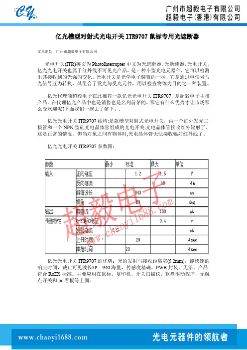
亿光槽型对射式光电开关ITR9707鼠标专用光遮断器
文章出处:广州市超毅电子有限公司
光电开关(ITR)英文为PhotoInterrupter中文为光遮断器,光断续器,光电开关。
亿光光电开关也属于红外线不可见光产品,是一种小型光电元器件,它可以检测出其接收到的光强的变化。
光电开关是光学电子装置的一种,它是通过电信号与光信号互为转换,其组合了发光与受光元件,用以检查物体为目的之一种装置。
亿光代理商超毅电子在此推荐一款亿光光电开关ITR9707,是超毅电子主推产品。
在代理亿光产品中也是销售也是名列前茅的,那它有什么优势才让市场那么受欢迎呢?下面我们一起去了解下。
.
亿光光电开关ITR9707结构:是款槽型对射式光电开关,由一个红外发光二极管和一个NPN型硅光电晶体管组成的光电开关,光电晶体管接收红外辐射了。
这是正常的情况。
但当对象之间有物体时,光电晶体管无法接收辐射红外线了。
亿光光电开关ITR9707参数图:
亿光光电开关ITR9707的优势:光的发射与接收距离宽(5.2mm),能快速的响应时间,截止可见波长λP=940海里,传感度精确,PWB封装,无铅,产品符合RoHS标准。
主要应用在鼠标,复印机,开关扫描仪,软盘驱动程序,无触点开关和pc看板等上面。
亿光光电开关ITR9707尺寸图:
亿光代理商超毅电子是亿光的15年合作伙伴,拥有着丰富的亿光光电开关的市场经验,因此,如果对于槽型对射式光电开关和反射式光电开关的相关应用资料跟规格参数,可直接联系超毅,超毅电子会为您提供最专业的技术支持。
免费咨询热线:4008-800-932。
韩国电子品牌 'OPTO-ELECTRONIC' 的817A型号光电耦合器说明书
Dimensions: [mm]121Scale - 3:1Würth Elektronik eiSos GmbH & Co. KG EMC & Inductive Solutions Max-Eyth-Str. 174638 Waldenburg Germany140817140110Würth Elektronik eiSos GmbH & Co. KGEMC & Inductive Solutions140817140110 Max-Eyth-Str. 174638 WaldenburgGermanyTotal Power Dissipation vs. Ambient Temperature:20406080100120140160-55-35-15525456585105125IR-diode -I F(mA)Ambient Temperature (°C)Phototransistor-PO(mW)CollectorPowerDissipation(mW)ForwardCurrent(mA)Collector Dark Current vs. Ambient Temperature:11010010001000025456585105125CollectorDarkCurrent(nA)Ambient Temperature (°C)V CE= 20VV CE= 10VNote: measured with Bin BWürth Elektronik eiSos GmbH & Co. KGEMC & Inductive SolutionsMax-Eyth-Str. 174638 WaldenburgGermanyCHECKED REVISION DATE (YYYY-MM-DD)GENERAL TOLERANCE PROJECTIONMETHODSaVo001.0052023-08-22DIN ISO 2768-1mDESCRIPTIONWL-OCPT OptocouplerPhototransistor ORDER CODE140817140110SIZE/TYPE BUSINESS UNIT STATUS PAGEAbsolute CTR vs. Ambient Temperature50100150200250300-60-40-20020406080100120AbsoluteCTRAmbient Temperature (°C)V CE= 5VV CE= 0,4VTestcondition: I F=5mA, T A=25°C, Bin BRelative CTR vs. Ambient Temperature:0,40,60,811,21,4-60-40-20020406080100120RelativeCTRAmbient Temperature (°C)V CE= 5VV CE= 0,4VTestcondition: I F=5mA, Normalized to T A=25°C, Bin BWürth Elektronik eiSos GmbH & Co. KGEMC & Inductive SolutionsMax-Eyth-Str. 174638 WaldenburgGermanyCHECKED REVISION DATE (YYYY-MM-DD)GENERAL TOLERANCE PROJECTIONMETHODSaVo001.0052023-08-22DIN ISO 2768-1mDESCRIPTIONWL-OCPT OptocouplerPhototransistor ORDER CODE140817140110SIZE/TYPE BUSINESS UNIT STATUS PAGEWürth Elektronik eiSos GmbH & Co. KGEMC & Inductive Solutions140817140110 Max-Eyth-Str. 174638 WaldenburgGermanyWürth Elektronik eiSos GmbH & Co. KGEMC & Inductive Solutions140817140110 Max-Eyth-Str. 174638 WaldenburgGermany050100150200250300350400450A b s o l u t e C T R (%)Testcondition T A Würth Elektronik eiSos GmbH & Co. KG EMC & Inductive Solutions Max-Eyth-Str. 174638 Waldenburg Germany140817140110050100150200250300A b s o l u t e C T R (%)Testcondition T A Würth Elektronik eiSos GmbH & Co. KG EMC & Inductive Solutions Max-Eyth-Str. 174638 Waldenburg Germany1408171401100102030R e s p o n s e T i m e (µs )Testcondition I C Würth Elektronik eiSos GmbH & Co. KG EMC & Inductive Solutions Max-Eyth-Str. 174638 Waldenburg Germany140817140110Würth Elektronik eiSos GmbH & Co. KGEMC & Inductive Solutions140817140110 Max-Eyth-Str. 174638 WaldenburgGermanyWürth Elektronik eiSos GmbH & Co. KGEMC & Inductive Solutions140817140110 Max-Eyth-Str. 174638 WaldenburgGermanyT e m p e r a t u r eT T T Würth Elektronik eiSos GmbH & Co. KG EMC & Inductive Solutions Max-Eyth-Str. 174638 Waldenburg Germany140817140110Cautions and Warnings:The following conditions apply to all goods within the product series of Optoelectronic Components of Würth Elektronik eiSos GmbH & Co. KG:General:•This optoelectronic component is designed and manufactured for use in general electronic equipment.•Würth Elektronik must be asked for written approval (following the PPAP procedure) before incorporating the components into any equipment in fields such as military, aerospace, aviation, nuclear control, submarine, transportation (automotive control, train control,ship control), transportation signal, disaster prevention, medical, public information network, etc. where higher safety and reliability are especially required and/or if there is the possibility of direct damage or human injury.•Optoelectronic components that will be used in safety-critical or high-reliability applications, should be pre-evaluated by the customer. •The optoelectronic component is designed and manufactured to be used within the datasheet specified values. If the usage and operation conditions specified in the datasheet are not met, the wire insulation may be damaged or dissolved. •Do not drop or impact the components, the component may be damaged•Würth Elektronik products are qualified according to international standards, which are listed in each product reliability report. Würth Elektronik does not warrant any customer qualified product characteristics beyond Würth Elektroniks’ specifications, for its validity and sustainability over time.•The responsibility for the applicability of the customer specific products and use in a particular customer design is always within the authority of the customer. All technical specifications for standard products also apply to customer specific products.•Unless Würth Elektroik has given its express consent, the customer is under no circumstances entitled to reverse engineer, disassemble or otherwise attempt to extract knowledge or design information from the optoelectronic component.Product specific:Soldering:•The solder profile must comply with the technical product specifications. All other profiles will void the warranty. •All other soldering methods are at the customers’ own risk•The soldering pad pattern shown above is a general recommendation for the easy assembly of optoelectronic components. If a high degree of precision is required for the selected application (i.e. high density assembly), the customer must ensure that the soldering pad pattern is optimized accordingly.Cleaning and Washing:•Washing agents used during the production to clean the customer application might damage or change the characteristics of the optoelectronic component body, marking or plating. Washing agents may have a negative effect on the long-term functionality of the product.• Using a brush during the cleaning process may break the optoelectronic component body. Therefore, we do not recommend using a brush during the PCB cleaning process.Potting:•If the product is potted in the customer application, the potting material might shrink or expand during and after hardening. Shrinking could lead to an incomplete seal, allowing contaminants into the optoelectronic component body, pins or termination. Expansion could damage the components. We recommend a manual inspection after potting to avoid these effects.Storage Conditions:• A storage of Würth Elektronik products for longer than 12 months is not recommended. Within other effects, the terminals may suffer degradation, resulting in bad solderability. Therefore, all products shall be used within the period of 12 months based on the day of shipment.•Do not expose the optoelectronic component to direct sunlight.•The storage conditions in the original packaging are defined according to DIN EN 61760-2.•For a moisture sensitive component, the storage condition in the original packaging is defined according to IPC/JEDEC-J-STD-033. It is also recommended to return the optoelectronic component to the original moisture proof bag and reseal the moisture proof bag again. •The storage conditions stated in the original packaging apply to the storage time and not to the transportation time of the components.Packaging:•The packaging specifications apply only to purchase orders comprising whole packaging units. If the ordered quantity exceeds or is lower than the specified packaging unit, packaging in accordance with the packaging specifications cannot be ensured.Handling:•Violation of the technical product specifications such as exceeding the nominal rated current, will void the warranty. •The product design may influence the automatic optical inspection.•Certain optoelectronic component surfaces consist of soft material. Pressure on the top surface has to be handled carefully to prevent negative influence to the function and reliability of the optoelectronic components.•ESD prevention methods need to be applied for manual handling and processing by machinery. •Resistors for protection are obligatory.•In addition to optoelectronic components testing, products incorporating these devices have to comply with the safety precautions given in IEC 60825-1, IEC 62471 and IEC 62778.Technical specification:•The typical and/or calculated values and graphics of technical parameters can only reflect statistical figures. The actual parameters ofeach single product, may differ from the typical and/or calculated values or the typical characteristic line.Würth Elektronik eiSos GmbH & Co. KG EMC & Inductive Solutions Max-Eyth-Str. 174638 Waldenburg GermanyCHECKED REVISION DATE (YYYY-MM-DD)GENERAL TOLERANCEPROJECTION METHODSaVo001.0052023-08-22DIN ISO 2768-1mDESCRIPTIONWL-OCPT Optocoupler PhototransistorORDER CODE140817140110SIZE/TYPEBUSINESS UNITSTATUSPAGE•In the characteristics curves, all values given in dotted lines may show a higher deviation than the paramters mentioned above. •On each reel, only one bin is sorted and taped. The bin is defined on the current transfer ratio.•In order to ensure highest availability, the reel binning of standard deliveries can vary. A single bin cannot be ordered. Please contact us in advance, if you need a particular bin sorting before placing your order.•These cautions and warnings comply with the state of the scientific and technical knowledge and are believed to be accurate and reliable. However, no responsibility is assumed for inaccuracies or incompleteness.The customer has the sole responsibility to ensure that he uses the latest version of this datasheet, which is available on Würth Elektronik’s homepage. Unless otherwise agreed in writing (i.e. customer specific specification), changes to the content of this datasheet may occurwithout notice, provided that the changes do not have a significant effect on the usability of the optoelectronic components.Würth Elektronik eiSos GmbH & Co. KG EMC & Inductive Solutions Max-Eyth-Str. 174638 Waldenburg GermanyCHECKED REVISION DATE (YYYY-MM-DD)GENERAL TOLERANCEPROJECTION METHODSaVo001.0052023-08-22DIN ISO 2768-1mDESCRIPTIONWL-OCPT Optocoupler PhototransistorORDER CODE140817140110SIZE/TYPEBUSINESS UNITSTATUSPAGEImportant NotesThe following conditions apply to all goods within the product range of Würth Elektronik eiSos GmbH & Co. KG:1. General Customer ResponsibilitySome goods within the product range of Würth Elektronik eiSos GmbH & Co. KG contain statements regarding general suitability for certain application areas. These statements about suitability are based on our knowledge and experience of typical requirements concerning the areas, serve as general guidance and cannot be estimated as binding statements about the suitability for a customer application. The responsibility for the applicability and use in a particular customer design is always solely within the authority of the customer. Due to this fact it is up to the customer to evaluate, where appropriate to investigate and decide whether the device with the specific product characteristics described in the product specification is valid and suitable for the respective customer application or not.2. Customer Responsibility related to Specific, in particular Safety-Relevant ApplicationsIt has to be clearly pointed out that the possibility of a malfunction of electronic components or failure before the end of the usual lifetime cannot be completely eliminated in the current state of the art, even if the products are operated within the range of the specifications.In certain customer applications requiring a very high level of safety and especially in customer applications in which the malfunction or failure of an electronic component could endanger human life or health it must be ensured by most advanced technological aid of suitable design of the customer application that no injury or damage is caused to third parties in the event of malfunction or failure of an electronic component. Therefore, customer is cautioned to verify that data sheets are current before placing orders. The current data sheets can be downloaded at .3. Best Care and AttentionAny product-specific notes, cautions and warnings must be strictly observed. Any disregard will result in the loss of warranty.4. Customer Support for Product SpecificationsSome products within the product range may contain substances which are subject to restrictions in certain jurisdictions in order to serve specific technical requirements. Necessary information is available on request. In this case the field sales engineer or the internal sales person in charge should be contacted who will be happy to support in this matter.5. Product R&DDue to constant product improvement product specifications may change from time to time. As a standard reporting procedure of the Product Change Notification (PCN) according to the JEDEC-Standard inform about minor and major changes. In case of further queries regarding the PCN, the field sales engineer or the internal sales person in charge should be contacted. The basic responsibility of the customer as per Section 1 and 2 remains unaffected.6. Product Life CycleDue to technical progress and economical evaluation we also reserve the right to discontinue production and delivery of products. As a standard reporting procedure of the Product Termination Notification (PTN) according to the JEDEC-Standard we will inform at an early stage about inevitable product discontinuance. According to this we cannot guarantee that all products within our product range will always be available. Therefore it needs to be verified with the field sales engineer or the internal sales person in charge about the current product availability expectancy before or when the product for application design-in disposal is considered. The approach named above does not apply in the case of individual agreements deviating from the foregoing for customer-specific products.7. Property RightsAll the rights for contractual products produced by Würth Elektronik eiSos GmbH & Co. KG on the basis of ideas, development contracts as well as models or templates that are subject to copyright, patent or commercial protection supplied to the customer will remain with Würth Elektronik eiSos GmbH & Co. KG. Würth Elektronik eiSos GmbH & Co. KG does not warrant or represent that any license, either expressed or implied, is granted under any patent right, copyright, mask work right, or other intellectual property right relating to any combination, application, or process in which Würth Elektronik eiSos GmbH & Co. KG components or services are used.8. General Terms and ConditionsUnless otherwise agreed in individual contracts, all orders are subject to the current version of the “General Terms and Conditions of Würth Elektronik eiSos Group”, last version available at .Würth Elektronik eiSos GmbH & Co. KGEMC & Inductive SolutionsMax-Eyth-Str. 174638 WaldenburgGermanyCHECKED REVISION DATE (YYYY-MM-DD)GENERAL TOLERANCE PROJECTIONMETHODSaVo001.0052023-08-22DIN ISO 2768-1mDESCRIPTIONWL-OCPT OptocouplerPhototransistor ORDER CODE140817140110SIZE/TYPE BUSINESS UNIT STATUS PAGE。
永光电子光电中断器 ITR8307 S17 TR8 技术数据表说明书
LifecyclePhase:
http:\\
Rev 2
Page: 2 of 10
Prepared date:2006/1/18
Prepared by: Ming-jing Lee
Release Date:2008-09-20 00:15:54.0
1000hrs 22pcs Limit
0/1
Storage
LjLower
5 Low Temperature TEMP.j-55Ċ
1000hrs 22pcs Specification 0/1
Storage
Limit
6 DC Operating Life IF=20mA
1000hrs 22pcs
0/1
DŽ
DŽ
LƸ
Everlight Electronics Co., Ltd. Device NojDRX-083-215
Revision : 2
LifecyclePhase:
http:\\
Rev 2
Page: 6 of 10
Prepared date:2006/1/18
---
Output
Dark Current
C-E Saturation Voltage
ICEO VCE(sat)
--- --- 100 nA VCE=10V
--- --- 0.4 V
IC=2mA
,Ee=1mW/cm2
Transfer Characteristics
Light Current Leakage Current Rise time
Rev 2
Page: 7 of 10
Prepared date:2006/1/18
亿光光藕EL817规格书
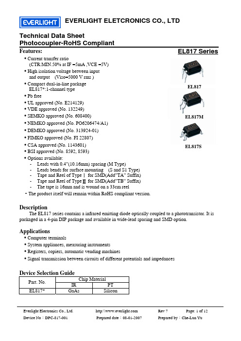
Photocoupler-RoHS Compliant EL817 SeriesFeatures: • Current transfer ratio(CTR:MIN.50% at IF =5mA ,VCE =5V) • High isolation voltage between input and output (Viso=5000 V rms ) • Compact dual-in-line package EL817*:1-channel type • Pb free• UL approved (No. E214129) • VDE approved (No. 132249) • SEMKO approved (No. 608400)• NEMKO approved (No. PO6206474/A1) • DEMKO approved (No. 313924-01)• FIMKO approved (No. FI 22807) • CSA approved (No. 1143601) • BSI approved (No. 8592, 8593) • Options available:- Leads with 0.4”(10.16mm) spacing (M Type)- Leads bends for surface mounting (S and S1 Type) - Tape and Reel of Type for SMD(Add”TA” Suffix)Ⅰ - Tape and Reel of Type Ⅱfor SMD(Add”TB” Suffix) - The tape is 16mm and is wound on a 33cm reel• The product itself will remain within RoHS compliant version.DescriptionThe EL817 series contains a infrared emitting diode optically coupled to a phototransistor. It is packaged in a 4-pin DIP package and available in wide-lead spacing and SMD option.Applications• Computer terminals• System appliances, measuring instruments• Registers, copiers, automatic vending machines• Signal transmission between circuits of different potentials and impedancesDevice Selection GuideChip MaterialPart. No.IR PTEL817* GaAs SiliconEL817EL817SEL817MPhotocoupler-RoHS CompliantEL817 SeriesPhotocoupler-RoHS CompliantEL817 SeriesS1 TypeNotes:1.Rank shall be or shall not be marked2.Factory code shall be marked (T: Taiwan / C: China)3.Year date code4.2-digit work week5.All dimensions are in millimeters6.Specifications are subject to change without noticePhotocoupler-RoHS Compliant EL817 SeriesAbsolute Maximum Ratings ( Ta=25°C )Parameter Symbol Rating UnitForward Current I F 50 mAPeak Forward Current*1I FM 1 A Input Reverse VoltageV R 6 V Power Dissipation P 70 mWCollector Power DissipationP C 150 mW Output Collector CurrentI C 50mA Collector-Emitter Voltage V CEO 35 V Emitter-Collector Voltage V ECO 6V Total Power DissipationPtot 200 mW *2Isolation Voltage Viso 5000 V rms Operating TemperatureTopr -55~+110 °C Storage TemperatureTstg -55~+125 °C *3Soldering TemperatureTsol260°C*1Frequency=100 HZ ,10uS Duty*2AC for 1 minute, R.H= 40~ 60%RH-Isolation voltage shall be measured using the following method. (1) Short between anode and cathode on the primary side and between collector, emitter and base on the secondary side.(2) The isolation voltage tester with zero-cross circuit shall be used. (3) The waveform of applied voltage shall be a sine wave*3For 10 secondsPhotocoupler-RoHS Compliant EL817 SeriesElectro-Optical Characteristics (Ta=25°C)Parameter Symbol Min. Typ. Max. Unit ConditionForward V F - 1.2 1.4 V I F =20mA Peak ForwardCurrent V FM 3.0 V I FM =0.5A Reverse Current I R - - 10 uAV R =4VInputTerminal Ct - 30 250 pF V=0,f=1kHz Collector Dark currentI CEO - - 100 nAV CE =20VOutputCollector- Emitter breakdown voltage BV CEO 35 - - V Ic=0.1mACurrent Transfer ratio CTR 50-600 % I F =5mA ,V CE =5VCollector- Emitter saturation voltageV CE(sat) - 0.1 0.2 V I F =20mA ,Ic=1 mAIsolation resistance R ISO 5×10¹⁰ 1011 - ΩDC500V,40~60%R.HFlotation capacitance Cf - 0.6 1.0 pF V=0, f=1MHz Cut-off frequency fc - 80 - kHz V CE =5V, I C =2 mAR L =100Ω, -3dBRise time t r - 4 18 us Transfer CharacteristicsFall timet f - 3 18 usV CE =2VI C =2mA,R L =100ΩPhotocoupler-RoHS CompliantEL817 Series SupplementCurrent Transfer Ratio CTRSub-Model No. Rank mark CTR (%) ConditionEL817* note 1 50 to 600EL817* (L) note2L 50 to 100EL817* (A) A 80 to 160EL817* (B) B 130 to 260 EL817* (C) C 200 to 400 EL817* (D) D 300 to 600 EL817* (AB) A or B 80 to 260 EL817* (BC) B or C 130 to 400 EL817* (CD) C or D 200 to 600 I F = 5 mA V CE = 5 V T a = 25°CNote1. The symbol “ * “ can be none or S or M by different leads form request Note2. The symbol “ ( ) ” can be CTR rankPhotocoupler-RoHS CompliantEL817 Series RELIABILITY PLANz The reliability of products shall be satisfied with items listed below.Confidence level : 90 % , LTPD : 10 %Classification Test Item Description & Condition (Acc.)Sample FailureCriteriaReferenceStandardOperation Life * Ta = 25±3°CIR: If = 50 mAPt: Pc = 130 mW ( Vf=1.4v) , 1000 hrs 0 / 22 MIL-S-750 : 1026MIL-S-883 : 1005JIS C 7021 : B-1High Temperature / High Humidity Reverse Bias (H3TRB) Ta = 85 ±3°C , Humi. = 85 % rhPt: 80% * Vce (max rating) , 1000 hrs0 / 22 JIS C 7021 : B-11High Temperature Reverse Bias (HTRB) Ta = 105 ±3°CPt: 100% * Vce (Max rating) ,1000 hrs0 / 22 JIS C 7021 : B-8Low Temperature Storage Ta = -50 ±3°C , 1000 hrs 0 / 22 JIS C 7021 : B-12High Temperature Storage Ta = 125 ±3°C , 1000 hrs 0 / 22 JIS C 7021 : B-10MIL-S-883 : 1008 Endurance testAuto clave P = 15 PSIG , Ta = 121 °C ,Humi. = 100 % rh , 48 hrs0 / 22 JESD 22-A102-BTemperature Cycling (Air to Air) 125°C ~ - 55 °C30 ~ 30 min , 100 cycles0 / 22 MIL-S-883 :1010JIS C 7021 : A-4Thermal Shock (Liquid to Liquid) 125 ~ - 55°Ct (dwell) = 5 mint (trans.) = 10 sec , 100 cycles0 / 22 MIL-S-202 : 107DMIL-S-750 : 1051MIL-S-883 :1011Solder Resistance Ta = 260 ±3°Ct (dwell) = 10 ±1 sec 0 / 22 MIL-S-750 : 2031JIS C 7021 : A-1Environmental TestSolder Ability Ta = 230 ±3 °Ct (dwell) = 5 ±1 sec 0 / 22CTR shift > 1.2Vf > U* 1.0Ir > U * 1.0Vce(sat) >U*1.0Bvceo < L*1.0Bveco < L*1.0L :LowSpec.LimitU : Up Spec.LimitMIL-S-883 : 2003JIS C 7021 : A-2Photocoupler-RoHS CompliantEL817 Seriesz Packing Quantity1.100 Pcs/ Per Tube2.25 Tubes / Inner Carton3.12 Inner Cartons / Outside Carton3. Outside Carton。