CdSe量子点的电荷存储
CdSe量子点敏化纳米TiO2太阳能电池的电化学交流阻抗谱省优质课赛课获奖课件市赛课一等奖课件

与DSSCs 相比, QDSSCs 旳电荷转移电阻相对较小,且向低偏压 方向位移
原因:Rct0 正比于exp[α(Ecb –EF0), 也就是说与化学电容相同, QDSSCs 旳电荷转移电阻向低偏压方向位移
位移旳幅度比化学电容位移幅度小, 原因:纳米TiO2 电极表面吸附半胱胺酸, 减缓了导带电子与氧
• 3)QDSSCs 旳暗态电子寿命和电子扩散长度比DSSCs 旳大, 与纳米TiO2 电极表面吸附半胱胺酸, 在一定程度上克制了 电子复合有关, 表白目前采用CQD 措施制备旳QDSSCs 短路 电流低旳主要原因不是纳米TiO2/电解质界面电子复合, 而 光吸收效率低是其中主要原因之
谢谢!
三 成果与讨论
QDSSCs 与DSSCs 旳总电阻Rtotal(未包括Rd)、 Rseries及Rpt图
与DSSCs相比, QDSSCs旳
串联电阻Rseries相对较大,
这是造成电池填充因子低 旳一种主要原因.
与Rs、Rt 相比, Rpt 对于串
联电阻具有主要贡献, 与 Mora-Seró 等旳分析成果 一致.
膜电极旳化学电容Cfilms由纳米多孔TiO2薄膜化学电容C 和 TCO/电解质旳界面化学电容CTCO. 在高偏压下,Cfilms主要取决于C ,暗态下,C 与外加偏 压Va旳关系为:
当0 < β < 1 时, 表白陷阱态成指数形式分布, 当β = 1 时, 阐明载流子均分布在导带内; Ecb、EF0分 别为纳米TiO2 旳导带边和外加偏压为0 时旳准费米能级
上
30min 450oC
多孔构造旳纳
米TiO2电极 TiO2板
CdSeCdS量子点的发光性能
CdSe/ CdS量子点发光特性
CdSe/ CdS量子点发光特性
发光特性
(1) 半导体量子点的发光性质可以通过改变量子点的尺寸来加以调 控。通过改变半导体量子点的尺寸和它的化学组成可以使其荧光 发射波长覆盖整个可见光区。 (2) 半导体量子点具有较大的斯托克斯位移(荧光光谱较相应的吸 收光谱红移)和较窄而且对称的荧光谱峰( 半高全宽只有40 nm) , 这样可以同时使用不同光谱特征的量子点, 而发射光谱不 出现交叠或只有很小程度的重叠, 使标记生物分子的荧光光谱的 区分、识别会变得更加容易。 (3) 半导体量子点具有较高的发光效率。
CdSe/ CdS量子点发光特性
CdSe/ CdS量子点发光特性
CdSe/CdS量子点发光特性
CdSe/CdS量子点在光电子学方面的应用 半导体量子点可以通过改变颗粒尺寸而获得不同的发射波长,发光 光谱较窄。因此将半导体量子点材料与有机/ 聚合物发光材料复合 用于电致发光器件, 来获得高色纯度、窄谱带以及在可见光范围内 发光峰连续可调的系列电致发光器件,使其在光电子器件方面展现 出广阔的应用前景。 用CdSe 量子点材料和聚合物材料PPV复合制备了双层结构的发光 器件, 发光颜色从红色调谐到黄色, 在较高电压时聚合物层PPV发出 的绿光占主要优势, 亮度可以达到100cd/m2。 将核壳结构的CdSe/ CdS半导体量子点用于有机无机复合结构的电 致发光器件 ITO/ PPV/ CdSe ( CdS) / Mg/Ag,其亮度可达600 cd/m, 电流密度为1A/cm,外量子效率可以达到0.22%,起亮电压为4 V,寿命 可以达到数百个小时, 而且发光颜色从红色变化到绿色, 与没有修饰 的CdSe量子点制成的相似的器件相比, 其量子效率和寿命都有明显 提高。
胶体CdSe/CdTe核壳Ⅱ型量子点敏化太阳能电池
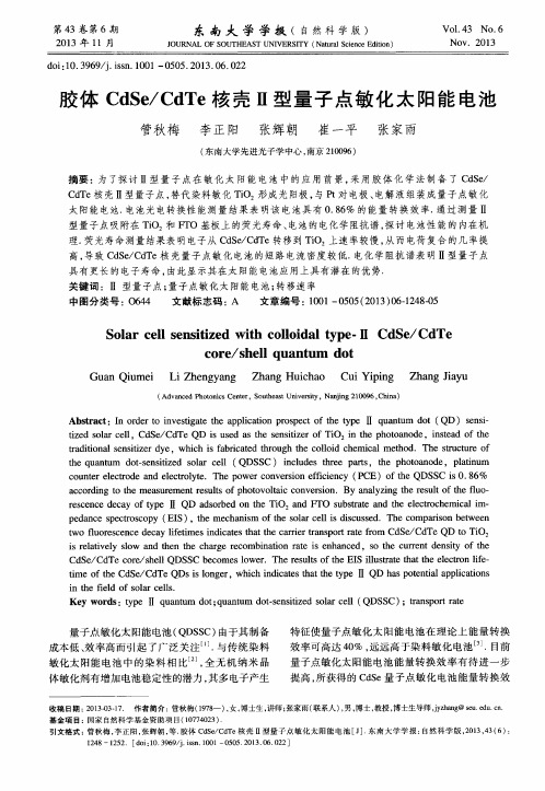
型量 子点 吸附在 T i O , 和F r O基 板上 的荧光寿 命 、 电池 的 电化 学 阻抗谱 , 探 讨 电池性 能 的 内在 机 理. 荧光寿命 测 量结果表 明电子从 C d S e / C d T e转 移到 T i O 上速 率较 慢 , 从 而 电荷 复合 的几 率提 高, 导致 C d S e / C d T e核 壳量子 点敏 化 电池 的短 路 电流 密度 较低 . 电化 学阻抗 谱表 明 Ⅱ型量 子 点
a c c o r d i n g t o t h e me a s u r e me n t r e s ul t s of ph o t ov o l t a i c c o n v e r s i o n. By a na l y z i n g he t r e s ul t o f he t f l uቤተ መጻሕፍቲ ባይዱ —
r e s c e n c e d e c a y o f t y p e 1 I Q D a d s o r b e d o n he t T i O nd a F T O s u b s t r a t e a n d he t e l e c t r o c h e m i c a l i m—
管秋梅 李正 阳 张辉朝 崔一平 张家雨
( 东 南 大学 先 进 光 子 学 中心 , 南京 2 1 0 0 9 6 )
摘 要 :为 了探讨 Ⅱ型 量 子 点在 敏 化 太 阳 能 电池 中 的 应 用 前 景 , 采用胶体化学法制备 了 C d S e /
C d T e核 壳 Ⅱ型量子 点 , 替代 染料 敏化 T i O 形 成光 阳极 , 与P t 对 电极 、 电解 液组 装成 量 子点敏 化
CdSe量子点的制备及其发光性能的研究的开题报告

CdSe量子点的制备及其发光性能的研究的开题报告
一、研究背景
随着纳米技术的不断发展,量子点作为一种新型半导体材料,由于其独特的物理和化学性质,备受关注。
CdSe作为一种具有优异光电性能的半导体材料,其量子点也成为研究热点之一。
本次研究旨在通过合成CdSe量子点并研究其发光性能,为其应用于生物标记、光电转换、激光器等领域奠定基础。
二、研究内容和方法
1. 合成CdSe量子点
通过改进热分解法制备CdSe量子点,利用Cd(OA)2和Se(DPM)2等化合物为前体,经过高温热解反应,得到CdSe量子点。
2. 表征CdSe量子点结构
利用X射线衍射仪、透射电子显微镜(TEM)、高分辨透射电子显微镜(HRTEM)等手段进行结构表征。
3. 研究CdSe量子点的荧光性质
利用紫外-可见吸收光谱仪、荧光光谱仪、时间分辨荧光光谱仪等装置研究CdSe量子点的荧光性质。
三、研究意义和预期结果
CdSe量子点具有很好的物理和化学性质,其应用范围广泛,包括生物成像、光电转换和传感等。
本次研究旨在合成CdSe量子点并研究其发光性能,进一步探究其荧光性质及应用前景,为其在相关领域的应用提供基础研究支持。
预期结果包括成功制备CdSe量子点、对其进行表征并研究其荧光性质,以及进一步探讨其应用前景。
关于量子点的相关知识综述
关于量子点的相关知识综述量子点(Quantum Dots)是指粒子直径尺寸小于激子波尔半径且具有明显量子效应的半导体纳米结构,也被称作半导体纳米晶。
它既可以由一种半导体材料制成,例如由Ⅱ-Ⅵ族元素(CdTe、CdS、ZnSe、CdSe等)或Ⅲ-Ⅴ族元素(InAs、InP等)组成,也可以由两种及两种以上的半导体纳米材料组成。
作为一种新型的半导体纳米材料,量子点具有很多优良的特性。
1.量子点的性质(1)量子点的发射光谱能够通过改变量子点的粒子尺寸大小来控制。
通过改变量子点的化学组成成分和粒径大小能够使其发射光谱遍布整个可见光区。
利用量子点的这一性质可以制备荧光光谱特征不同的量子点。
(2)量子点有着很好的光稳定性相比于传统的荧光试剂。
量子点的荧光强度和稳定性比起传统有机荧光材料罗丹明6G强好几十倍以上。
因此量子点在生物标记方面有着广泛的应用,为研究长期相互作用的分子之间提供了重要的作用。
(3)量子点同时具有宽且连续的激发光谱和窄的发射光谱。
利用同一激发光源即可对不同尺寸的量子点进行同步检测,因此可以用作多色标记,极大地促进和发挥了荧光标记的应用。
(4)量子点具有较大的期托克斯位移[8]。
期托克斯位移(Stokes shift)是指量子点的最大紫外吸收峰位与荧光发射峰位所对应的波长之间的差值。
量子点的另一个优异的光学性质就是其具有宽的期托克斯位移,这是量子点显著的光谱特性,这样可以避免发射光谱与激发光谱的重叠,有利于荧光光谱信号的检测。
图1 斯托克斯位移示意图(5)量子点有着极好的生物相容性。
量子点经过各种化学修饰以后,不但能够提高它的光稳定性和量子产率[9, 10],而且有利于进行特异性结合,另外其毒性较低,对其他生物体的危害小,可以进行生物活体的标记和检测。
(6)量子点具有很长的荧光寿命。
量子点的荧光寿命可持续数十纳秒,相比于有机荧光染料的寿命几纳秒[11]长很多,当进行光激发以后,多数物质的自发荧光会发生衰变,而量子点的荧光却依旧存在,此时即可采集到无背景干扰的荧光信号。
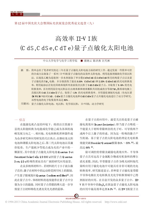
高效率 CdS CdSe CdTe 量子点敏化太阳电池
三 量子点敏化电极的制备方法 传统的量子点敏化电极的制备方法可大致分
为间接和原位制备法两类。 间接合成中多用直接吸附法(Direct Adsorption,
DA)[23~26]或分子链接法(Linker-Assisted Adsorption, LA)[13,27~30]先在较高温度下通过热注入法快速制备 量子点,量子点结晶度高且尺寸分布窄,表面缺陷 较少。但由于表面长链修饰剂去除或置换不完全 以及溶剂极性不匹配等原因,TiO2 纳米颗粒表面
23 SOLAR ENERGY 1/2013
SOLAR ENERGY
太 阳 能 技术产品与工程
的量子点负载率很低,且量子点易聚集,严重影响 敏化电池的光吸收性质[23]。虽在对制备体系进行 了一定的改良后,电池效率提升明显,但相比原位 法制备的量子点敏化电池的效率仍有较大差距。
原位制备方法中使用最为普遍的是化学浴沉 积法(Chemical Bath Deposition, CBD)[8,31,32]和连续 离子层吸附生长法(Successive Ionic Layer Adsorption and Reaction, SILAR)[33~36]。这两种方法克服 了直接吸附法和分子链接法中量子点负载率低和 有机分子导电性差等缺点,使大量量子点直接与 TiO2 基底接触,提高了 QDSSCs 的吸光强度,且 能使法仍存在较大缺陷:获得的量子点具有非常宽的 尺寸分布,量子点的结晶度也较差,造成了大量可 能引起光生电子复合的表面态[37];且两种方法均 适于在大气环境下操作,在稳定性较差的量子点 (如 CdTe)的合成中受到限制。
敏化电极,并将其应用于量子点敏化太阳电池。其 中双官能团分子在反应过程中可发挥稳定剂、连 接剂以及硫源的作用。研究中发现控制温度可调 控量子点的尺寸和覆盖率,且在较高温度下获得 具有 CdS 壳层的 II型核壳量子点。实验证明,CdS 壳层除可保护 CdTe 或 CdSe 晶核不被氧化外,还 可促进电荷分离,减少电子复合,有利于提高量子 点敏化太阳电池的光电转换效率。此外,CdTe/ CdS 和CdSe/CdS核壳量子点敏化电池还由于合适 的粒径大小和在 TiO2 表面较亮的覆盖率增强了对 光的利用,分别获得了最高3.80%和 2.83%的光电 转换效率。其中3.80%的光电转换效率是目前基于 CdTe 量子点敏化太阳电池的文献报道的最高值。
CdSe量子点简要综述2

CdSe量子点综述量子点(quantum dots, QDs)是一种半导体纳米晶(nanocrystals, NCs)通常由Ⅱ-Ⅱ和Ⅱ-Ⅱ族元素组成,如CdSe、CdTe、ZnSe、CuInS、InP等。
也可以由两种或两种上的半导体材料构成,如核壳结构的CdSe/ZnS、CdSe/CdZnS等,以及掺杂结构的ZnS:Mn,ZnSe:Cu等。
1.量子点结构常见的二元半导体量子点由于覆盖光谱有限且稳定性不高,易受外界环境物理化学的影响而发生质量退化,因此,常通过制备合金量子点或核壳结构量子点来改善量子点的物理化学性质错误!未找到引用源。
1.1合金量子点合金量子点即将几种不同带隙的半导体材料在纳米尺度上进行的合金化,形成合金或固溶体。
由于每种半导体材料都有其相应的能带宽,通过形成合金通过调节合金半导体组分的化学计量比来改变纳米晶的组成,从而改变量子点的能带宽及晶格常数。
此类量子点也可按照组成元素的多少分为三元合金和多元合金。
要制备均匀结构的合金,两种组成的生长速率必须相等,并且在一种成分的生长的条件下不能阻止另一种成分的生长,同时两种成分需要充分相似使得两者容易混合,否则会形成核壳结构或者两种组分独立成核。
1.2核/壳结构量子点根据各种半导体材料能带位置的不同,壳层在核/壳结构量子点中起到作用的不同,可以将核/壳量子点分为三类:TypeⅡ、TypeⅡ和TypeⅡ型结构,如图1.1所示。
图1.1 半导体异质结的能带结构TypeⅡ型结构的量子点要求壳层材料能带大于核层材料能带,电子和空穴都被限域在核材料中,从而提高量子点的荧光效率,但也有相反的情况;TypeⅡ型结构的量子点要求壳层材料的价带或导带处于核层材料的带隙中,通过光子的激发,壳层材料能带的重叠导致电子和空穴的空间分离而分别处于核层材料和壳层材料中;TypeⅡ型结构很少应用到核壳量子点结构中去。
TypeⅠ型结构是最早被研究的结构,该结构中宽能带的壳层材料所起的作用是钝化核层材料的表面缺陷,使核材料与外部环境隔离,将载流束缚在核中。
CdSe量子点简要综述2
CdSe量子点综述量子点(quantum dots, QDs)是一种半导体纳米晶(nanocrystals, NCs)通常由Ⅱ-Ⅱ和Ⅱ-Ⅱ族元素组成,如CdSe、CdTe、ZnSe、CuInS、InP等。
也可以由两种或两种上的半导体材料构成,如核壳结构的CdSe/ZnS、CdSe/CdZnS等,以及掺杂结构的ZnS:Mn,ZnSe:Cu等。
1.量子点结构常见的二元半导体量子点由于覆盖光谱有限且稳定性不高,易受外界环境物理化学的影响而发生质量退化,因此,常通过制备合金量子点或核壳结构量子点来改善量子点的物理化学性质错误!未找到引用源。
1.1合金量子点合金量子点即将几种不同带隙的半导体材料在纳米尺度上进行的合金化,形成合金或固溶体。
由于每种半导体材料都有其相应的能带宽,通过形成合金通过调节合金半导体组分的化学计量比来改变纳米晶的组成,从而改变量子点的能带宽及晶格常数。
此类量子点也可按照组成元素的多少分为三元合金和多元合金。
要制备均匀结构的合金,两种组成的生长速率必须相等,并且在一种成分的生长的条件下不能阻止另一种成分的生长,同时两种成分需要充分相似使得两者容易混合,否则会形成核壳结构或者两种组分独立成核。
1.2核/壳结构量子点根据各种半导体材料能带位置的不同,壳层在核/壳结构量子点中起到作用的不同,可以将核/壳量子点分为三类:TypeⅡ、TypeⅡ和TypeⅡ型结构,如图1.1所示。
图1.1 半导体异质结的能带结构TypeⅡ型结构的量子点要求壳层材料能带大于核层材料能带,电子和空穴都被限域在核材料中,从而提高量子点的荧光效率,但也有相反的情况;TypeⅡ型结构的量子点要求壳层材料的价带或导带处于核层材料的带隙中,通过光子的激发,壳层材料能带的重叠导致电子和空穴的空间分离而分别处于核层材料和壳层材料中;TypeⅡ型结构很少应用到核壳量子点结构中去。
TypeⅠ型结构是最早被研究的结构,该结构中宽能带的壳层材料所起的作用是钝化核层材料的表面缺陷,使核材料与外部环境隔离,将载流束缚在核中。
- 1、下载文档前请自行甄别文档内容的完整性,平台不提供额外的编辑、内容补充、找答案等附加服务。
- 2、"仅部分预览"的文档,不可在线预览部分如存在完整性等问题,可反馈申请退款(可完整预览的文档不适用该条件!)。
- 3、如文档侵犯您的权益,请联系客服反馈,我们会尽快为您处理(人工客服工作时间:9:00-18:30)。
Organic bistable devices based on core/shell CdSe/ZnS nanoparticles embedded in a conducting poly …N -vinylcarbazole …polymer layerFushan Li,Dong-Ik Son,Seung-Mi Seo,Han-Moe Cha,Hyuk-Ju Kim,Bong-Jun Kim,Jae Hun Jung,and Tae Whan Kim a ͒Advanced Semiconductor Research Center,Division of Electronics and Computer Engineering,Hanyang University,17Haengdang-dong,Seongdong-gu,Seoul 133-791,Korea͑Received 16July 2007;accepted 16August 2007;published online 21September 2007͒Current-voltage measurements on the Al/͓CdSe/ZnS nanoparticles embedded in a hole-transporting poly ͑N -vinylcarbazole ͒͑PVK ͒layer ͔/indium tin oxide ͑ITO ͒/glass structures at 300K showed a nonvolatile electrical bistability behavior.Capacitance-voltage ͑C -V ͒measurements on the Al/͓CdSe/ZnS nanoparticles embedded in a PVK layer ͔/ITO/glass structures at 300K showed a metal-insulator-semiconductor behavior with a flatband voltage shift due to the existence of the CdSe/ZnS nanoparticles,indicative of trapping,storing,and emission of charges in the electronic states of the CdSe nanoparticles.Operating mechanisms for the Al/͓CdSe/ZnS nanoparticles embedded in the PVK layer ͔/ITO/glass devices are described on the basis of the C -V results.©2007American Institute of Physics .͓DOI:10.1063/1.2783189͔Organic structures containing inorganic nanoparticles have been particularly attractive due to interest in their prom-ising applications in electronic and optoelectronic devices 1–7because of their unique advantages of low-power consump-tion,high mechanical flexibility,and chemical structural ver-satility.Such hybrid organic/inorganic devices are also excel-lent candidates for potential applications in next-generation transistor and memory devices.8,9Potential applications of memory devices utilizing nanoparticles embedded in organic layers have driven extensive effort to form various kinds of nanoparticles.10,11Even though some studies concerning the formation of metal nanoparticles embedded in an organic layer for applications such as nonvolatile organic bistable devices ͑OBDs ͒have been conducted,almost all of the devices were fabricated by using strin-gent high-vacuum evaporation method.12–14The memory effects of core/shell-type cadmium selenium ͑CdSe ͒nano-particles embedded in a conducting poly ͓2-methoxy-5-͑2-ethylhexyloxy ͒-1,4-phenylene-vinylene ͔͑MEH-PPV ͒poly-mer fabricated by using a simple spin-coating technique were reported.15Because the narrow band gap of MEH-PPV leads to a low charge capturing efficiency,resulting in the realization of memory effect at a high bias voltage of 10V,a hole transport poly ͑N -vinylcarbazole ͒͑PVK ͒matrix can be introduced here to obtain the memory effects in CdSe/PVK nanocomposites under an applied bias voltage as small as 2V.Furthermore,studies on the memory effects and their operating mechanisms for OBDs made of semiconductor nanoparticles embedded in a conducting polymer are very important for improving the efficiencies of nonvolatile flash memories.This letter reports data for the bistability and the operat-ing mechanisms of the memory effects of OBDs fabricated utilizing CdSe semiconductor nanoparticles embedded in a PVK polymer layer.Core/shell-type CdSe nanoparticles have become particularly attractive because of their promising ap-plications in next-generation nonvolatile flash memory de-vices with low-power and ultrahigh-density elements.16,17Current-voltage ͑I -V ͒measurements were carried out to in-vestigate the electrical bistable properties of the fabricated OBDs containing CdSe/ZnS nanoparticles embedded in the PVK layer.Capacitance-voltage ͑C -V ͒measurements were carried out to investigate the possibility of fabricating memory effects involving the CdSe/ZnS nanoparticles em-bedded in the PVK layer.Furthermore,the dependence of the memory effects on the thickness of the PVK layer containing CdSe/ZnS nanoparticles was also investigated.The CdSe/ZnS nanoparticles with a diameter of about 6nm were purchased commercially,and a schematic dia-gram of the core/shell-type CdSe/ZnS nanoparticles is shown in Fig.1͑a ͒.The device with a structure shown in Fig.1͑b ͒was fabricated through the following process:At first,the indium tin oxide ͑ITO ͒coated glass acting as a hole-injection layer in the OBDs was alternately cleaned with a chemical cleaning procedure by using trichloroehylene,ac-etone,and methanol solutions.Then,the PVK layer contain-ing the CdSe/ZnS nanoparticles was formed by spin coating a chloroform solution of 1.3%by weight PVK and 0.5%by weight CdSe/ZnS nanoparticles.Finally,a top Al electrode layer with a thickness of about 800nm was deposited by thermal evaporation.The I -V and C -V measurements were performed by using an HP 4284precision LCR meter at room temperature.Figure 2shows I -V curves for the Al/͑CdSe/ZnS nano-particles embedded in the PVK layer ͒/ITO/glass OBD struc-a ͒Author to whom correspondence should be addressed;electronic mail:twk@hanyang.ac.kr FIG.1.Schematic diagrams of the CdSe/ZnS nanoparticles and the fabri-cated device studied in this study.APPLIED PHYSICS LETTERS 91,122111͑2007͒0003-6951/2007/91͑12͒/122111/3/$23.00©2007American Institute of Physics 91,122111-1Downloaded 22 Oct 2007 to 166.104.58.178. Redistribution subject to AIP license or copyright, see /apl/copyright.jspture with a 500-nm-thick active layer.The I -V curve under a forward bias voltage,denoted by the empty rectangles in the lower curve of the Fig.2,shows a dramatic increase in the injection current at about 1V,indicative of a bistable tran-sition of the device from a low-conductivity state ͑off state ͒to a high-conductivity state ͑on state ͒.The bistable transition from the off state to the on state is equivalent to the “writing”process in a digital memory cell.18After that transition is finished,the on state remains in the device even after turning off the power,which is shown in the reverse bias voltage denoted by the filled rectangles in the upper curve of Fig.2.Figure 2clearly shows an electrical hysteresis behavior,which is an essential feature for bistable devices,and reveals the nonvolatile nature of the memory effect.19While the cur-rent difference between the on and off states for the PVK only device is negligible,the bistability in the Al/͑CdSe/ZnS nanoparticles embedded in the PVK layer ͒/ITO/glass device might be attributed to the screening of the applied electric field due to the existence of the internal electric field gener-ated by the captured charge carriers in the CdSe nanopar-ticles.The off state can be recovered by applying a reverse bias voltage.This is equivalent to the “erasing”process of a digital memory cell resulting from the discharge of CdSe nanoparticles.The solid line in Fig.2corresponds to the I -V curve of the device after the application of a −2V bias and is almost identical to the I -V curve denoted by the empty square.The observation that the OBD device main-tains an on state at a reverse applied voltage is similar to those reported for an Al/2-amino-4,5-imidazoledicarbonitrile ͑AIDCN ͒organic/Al layer/AIDCN organic/Al system 18and an Al/AIDCN organic/Al nanoclusters/AIDCN organic/Al system.19The C -V curves measured at 1MHz for the Al/͑CdSe/ZnS nanoparticles embedded in the PVK layer ͒/ITO/glass OBD structure are shown in Fig.3.The C -V curve shows a metal-insulator-semiconductor ͑MIS ͒behavior with charge trap regions,and the C -V behavior is similar to that of MIS memories with floating gates containing Si nanocrystals.20,21A clockwise hysteresis is clearly observedin the C -V characteristics,indicative of the existence of sites occupied by charges.The presence of such sites is attributed to carrier charging and discharging in the CdSe/ZnS nano-particles.The flatband voltage shift of the C -V curve for the OBDs with a relatively thinner hybrid layer of 500nm,which originates from charge accumulation and depletion due to variations in the applied voltage,is approximately 3V,as shown in Fig.2͑a ͒,which is enough to capture car-riers inside the nanoparticles.The C -V curve for samples without CdSe nanoparticles under identical measurement conditions showed no hysteresis.Therefore,the hysteresis appearing in Fig.2may be attributed to carriers trapped in the embedded CdSe/ZnS nanoparticles,a clear indication of the memory effect.21The flatband voltage shift of the C -V curve decreases to approximately 1.5V with increasing thickness of the hybrid active layer to about 900nm,as shown in Fig.2͑b ͒.These results indicate that the flatband voltage shift of the C -V curve related to the magnitude of the memory is significantly affected by the thickness of the hy-brid active layer.When a positive voltage is applied,after the injection of holes from the ITO into the highest occupied molecular or-bital ͑HOMO ͒level occurs through the Fowler-Nordheim tunneling process,the holes existing at the HOMO level are transported along the direction of the applied voltage through the hopping mechanism among the PVK molecules.22AnFIG. 2.Current-voltage curves for the Al/͑CdSe/ZnS nanoparticles embedded in a PVK layer ͒/ITO/glass device.The scanning step of the applied voltage is 0.01V.Empty and filled rectangles represent the current-voltage curves of the forward and the reverse applied bias volt-ages,respectively.The solid line indicates the current-voltage curve after application of a reverse voltage pulse of −2V.FIG. 3.Capacitance-voltage curves for the Al/͑CdSe/ZnS nanoparticles embedded in PVK layer ͒/ITO/glass devices with the active layer thicknesses of ͑a ͒500nm and ͑b ͒900nm.Downloaded 22 Oct 2007 to 166.104.58.178. Redistribution subject to AIP license or copyright, see /apl/copyright.jspintuitive proposal is that the holes actually encounter CdSe/ZnS nanoparticles which are traversing the sample,and with increasing electrical field to a certain value,holes can tunnel through the ZnS shell into the valence band of the CdSe nanoparticles,as shown in Fig.4,resulting in the for-mation of an internal electric field along the direction of the applied voltage.Because the capacitance of the device ex-hibits a larger decrease in comparison with the capacitance in the depletion layer formed in the ITO substrate under a posi-tive bias voltage,the C -V curve of the device shifts to the left,as shown in Fig.2.When a negative voltage is applied to the electrode,because the holes captured in the valence band of the CdSe nanoparticles under the negative electric field are released into the PVK matrix and then transported to the ITO substrate,the erasing process is performed.Since the generated internal electric field disappears due to the re-lease of the holes captured in the CdSe/ZnS nanoparticles,the C -V curve of the device shifts to the right,as shown in Fig.3.Because the flatband voltage shift for the Al/͑CdSe/ZnS nanoparticles embedded in the PVK layer ͒/ITO/glass device is significantly affected by the thickness of the PVK layer containing CdSe nanoparticles,the magnitude of the memory effects can be moderately adjusted by varying the thickness of the active layer in the devices,which might be very im-portant for practical applications in memory devices.A simple mechanism for the dependence of the memory effects on the thickness of the PVK layer in which the CdSe/ZnS nanoparticles are embedded can be proposed.The probability of the charges being trapped by the CdSe/ZnS nanoparticles embedded in the PVK layer through the tunneling process is typically determined by the electric field at the organic/inorganic interface.23A smaller number of the holes in the OBDs will be captured by the CdSe/ZnS nanoparticles due to the smaller electric field resulting from an increase in thickness.Therefore,a smaller flatband voltage shift is attrib-uted to a decrease in the internal electric field generated by the trapped charges.In summary,the bistability and the operating mecha-nisms of an organic/inorganic hybrid device consisting of CdSe/ZnS nanoparticles and a PVK composite were inves-tigated.The I -V curves at ambient temperature for the Al/͑CdSe/ZnS nanoparticles embedded in the PVK layer ͒/ITO/glass devices exhibited a nonvolatile electrical bistable be-havior.The C -V curve at room temperature for the Al/͑CdSe/ZnS nanoparticles embedded in the PVK layer ͒/ITO/glass capacitors showed a MIS behavior with a large flatband voltage shift due to the existence of the CdSe/ZnS nanopar-ticles,indicative of trapping,storing,and emission of holes in the electronic states of the CdSe nanoparticles.The mag-nitude of the flatband voltage shift was significantly affected by the thickness of the PVK layer containing CdSe/ZnS nanoparticles,and a possible operating mechanism corre-sponding to the writing and erasing processes of memory devices was described on the basis of the C -V results.These results indicate that OBDs fabricated utilizing CdSe/ZnS nanoparticles embedded in PVK layers hold promise for po-tential applications in next-generation nonvolatile memories.This work was supported by the Korea Science and En-gineering Foundation ͑KOSEF ͒grant funded by the Korea government ͑MOST ͒͑No.R0A-2007-000-20044-0͒.1H.Sirringhaus,N.Tessler,and R.H.Friend,Science 280,1741͑1998͒.2C.D.Dimitrakopoulos and P.R.L.Malefant,Adv.Mater.͑Weinheim,Ger.͒14,99͑2002͒.3C.D.Muller and Aurelie Falcou,Nature ͑London ͒421,829͑2003͒.4A.C.Mayer,D.J.Herman,T.G.Kasen,and G.G.Malliaras,Appl.Phys.Lett.85,6272͑2004͒.5S.Yoo,B.Domercq,and B.Kippelen,Appl.Phys.Lett.85,5427͑2004͒.6F.Li,Z.Chen,C.Liu,and Q.Gong,Chem.Phys.Lett.412,331͑2005͒.7R.Könenkamp,R.C.Word,and M.Godinez,Nano Lett.5,2005͑2005͒.8L.Bakueva,S.Musikhin,M.A.Hines,T.-W.F.Chang,M.Tzolov,G.D.Scholes,and E.H.Sargent,Appl.Phys.Lett.82,2895͑2003͒.9J.H.Jung,J.H.Kim,T.W.Kim,C.S.Yoon,Y .-H.Kim,and S.Jin,Appl.Phys.Lett.89,022112͑2006͒.10X.Li,Y .Wu,D.Steel,D.Gammon,T.H.Stievater,D.S.Katzer,D.Park,C.Piermarocchi,and L.J.Sham,Science 301,809͑2003͒.11J.Heitmann,F.Müller,M.Zacharias,and U.Gösele,Adv.Mater.͑Wein-heim,Ger.͒17,795͑2005͒.12S.Moller,C.Perlov,W.Jackson,C.Taussig,and S.R.Forrest,Nature ͑London ͒426,166͑2003͒.13D.Ma,M.Aguiar,J.A.Freire,and I.A.Hummelgen,Adv.Mater.͑Wein-heim,Ger.͒12,1063͑2000͒.14J.H.Kim,J.Y .Jin,J.H.Jung,I.Lee,T.W.Kim,S.K.Lim,C.S.Yoon,and Y .-H.Kim,Appl.Phys.Lett.86,032904͑2005͒.15Fushan Li,Dong-Ick Son,Han-Moe Cha,Seung-Mi Seo,Bong-Jun Kim,Hyuk-Ju Kim,Jae-Hun Jung,and Tae-Whan Kim,Appl.Phys.Lett.90,222109͑2007͒.16E.Kapetanakis,P.Normand,D.Tsoukalas,and K.Beltsios,Appl.Phys.Lett.80,2794͑2002͒.17M.Perego,S.Ferrari,M.Fanciulli,G. B.Assayag, C.Bonafos,M.Carrada,and A.Claverie,J.Appl.Phys.95,257͑2004͒.18L.P.Ma,J.Liu,and Y .Yang,Appl.Phys.Lett.80,2997͑2002͒.19L.P.Ma,S.M.Pyo,J.Y .Ouyang,Q.Y .Xu,and Y .Yang,Appl.Phys.Lett.82,1419͑2003͒.20S.Huang,S.Banerjee,R.T.Tung,and S.Oda,J.Appl.Phys.94,7261͑2003͒.21S.J.Lee,Y .S.Shim,H.Y .Cho,D.Y .Kim,T.W.Kim,and K.L.Wang,Jpn.J.Appl.Phys.,Part 142,7180͑2003͒.22X.Y .Zhu,J.Phys.Chem.B 108,8778͑2004͒.23K.R.Choudhury,M.Samoc,A.Patra,and P.N.Prasad,J.Phys.Chem.B 108,1556͑2004͒.24Hedi Mattousssi,Leonard H.Radzilowski,Bashir O.Dabbousi,Edwin L.Thomas,Moungi G.Bawendi,and Michael F.Rubner,J.Appl.Phys.83,7965͑1998͒.FIG.4.Schematic diagram of the electronic structures corresponding to the operating mechanism for the Al/͑CdSe/ZnS nanoparticlesem-bedded in a PVK layer ͒/ITO/glass device under a positive bias voltage.The energy levels for the core/shell-type CdSe/ZnS nanoparticles are taken from the literature of Ref.24.Downloaded 22 Oct 2007 to 166.104.58.178. Redistribution subject to AIP license or copyright, see /apl/copyright.jsp。