MYC-AM335X核心板引脚定义说明列表
AM335x 处理器 SDK RTOS 板库端口和启动说明书

Board Porting\Bring up using Processor SDK RTOS for AM335xProcessor SDK RTOS component known as board library consolidates all the board-specific information so that all the modifications made when moving to a new custom platform using the SOC can be made in the source of this library.There are three different components in PRSDK that help in porting and bring up of a custom board:∙Board library updatesa.PLL Clocking and PRCMb.Pin mux Updatec.DDR Configurationd.Peripheral instances updates∙Diagnostics tests∙Boot loader updatesBoard Library Updates in Processor SDK RTOS:PLL ClockingThere are two places where the device PLL configurations are performed when using Processor SDK RTOS and CCS.Debug environment:Debug environment refers to development setup where code is debugged using JTAG emulator on the SOC. The PRSDK software relies on the GEL file that is part of the target configuration to setup the clocks and the DDR for the device. The CCS GEL file for AM335x platforms is located in the CCS package at the location ccsv7\ccs_base\emulation\boards\<boardName>For example for beagle bone black, the files can be found atccsv7\ccs_base\emulation\boards\beaglebone\gelThe GEL is the first piece of software that should be brought up on a custom board.Production environment:Production environment refers to the setup when the base application is booted from a boot media like a flash memory or host interface. In this environment, the bootloader sets performs all the SOC and board initialization and copies the application from flash memory to the device memory.The clock setup in the bootloader code can be located atpdk_am335x_x_x_x\packages\ti\starterware\bootloader\src\am335xUsers can choose to use the platform clocking similar to one of TI reference platforms or can modify them as per their application requirements. By default the PLL settings are setup for OPP_NOM settings (MPU= 600 MHz.)TI provides Clock Tree tool to allow users to simulate the clocking on the SOC. For quick reference of the multiplier and divider settings to change the PLL setting is provided in the spreadsheetAM335x_DPLL_CALCv3.xlsx.After modifying the clocking in the bootloader, users need to rebuild the bootloader using instructions provided in Processor_SDK_RTOS_BOOT_AM335x/AM437xPRCM Modules Enable:PRCM Module Enable is required to turn on the power domain and the clocking to each of the modules on the SOC. The PRCM Enable calls to enable each module are made from the functionBoard_moduleClockInit which is found in the location.pdk_am335x_1_0_9\packages\ti\board\src\bbbAM335x\bbbAM335x.cCheck every instance and peripheral required in the application platform and enable the module in the board library.For example to use three UARTs 0, 1 and 4, ensure that you have the following code as part of the board library setup:/* UART */status = PRCMModuleEnable(CHIPDB_MOD_ID_UART, 0U, 0U);status = PRCMModuleEnable(CHIPDB_MOD_ID_UART, 1U, 0U);status = PRCMModuleEnable(CHIPDB_MOD_ID_UART, 4U, 0U);Note: PRCMEnable function is defined in pdk_am335x_1_0_9\packages\ti\starterware\soc\am335x Pinmux updates in the Board library:Generating a New PinMux Configuration Using the PinMux Utility: This procedure uses the cloud-based pinmux utilityNavigate to ${PDK_INSTALL_DIR}\packages\ti\starterware\tools\pinmux_config\am335x and Load beaglebone_black_configAdd and remove peripheral instances and select the appropriate use cases required for development based on the application platform requirements and resolve all conflicts.Refer Pin_Mux_Utility_for_ARM_MPU_ProcessorsPost Processing steps:1.Change the Category filter to starterware and download the pinmux files am335x_pimnmux.hand am335x_pinmux_data.c2.At the bottom of am335x_pinmux.h change extern pinmuxBoardCfg_t gAM335xPinmuxData[];to extern pinmuxBoardCfg_t gBbbPinmuxData[];3.Change am335x_pinmux_data.c to am335x_beagleboneblack_pinmux_data.c.4.Change gAM335xPinmuxData to gBbbPinmuxData at the end of the file in file5.am335x_beagleboneblack_pinmux_data.c.Replace the existing files with the new files and rebuild the board library using the instructions in the section Rebuilding board Library in Processor SDK RTOS:Updating DDR settings:Similar to clock and PLL settings, DDR initialization is configured in the Debug environment through GEL files and in production environment using bootloader source files.TI provides AM335x_EMIF_Configuration_tips which contains a spreadsheet to enter the timing from the DDR datasheet to compute the EMIF timing number required to initialize DDR.We strongly recommend changing the value and testing using GEL files before using them in the bootloader software. For Sanity test, you can perform read/write tests using CCS Memory Browser or run the diagnostic memory read/write test that we provide in diagnostics package here:PDK_INSTALL_PATH\packages\ti\board\diag\memOnce the DDR timings have been confirmed, you can use the settings in the file:PDK_INSTALL_PATH \packages\ti\starterware\bootloader\src\am335x\sbl_am335x_platform_ddr.c Peripheral initialization:The board library is responsible for most of the SOC initialization but it also setup some board level components such as ethernet PHY and debug UART and I2C for reading board ID from EEPROM. All of the other peripheral instances and initialization needs to be done from the application level.For example for beagleboneblack, the peripheral initialization are performed from the source filepdk_am335x_1_0_9\packages\ti\board\src\bbbAM335x\bbbAM335x_lld_init.cThe debug UART instance, I2C Addresses are set using the file board_cfg.h found under:pdk_am335x_1_0_9\packages\ti\board\src\bbbAM335x\includeDefault UART instance is set to 0 in the board library. The Board initialization will configure the UART instance 0 to send binary log data to serial console using the Board_UARTInit function. If you wish to use more UART instances then we recommend linking in the UART driver in the application and using UART_open() and UART_stdioInit API calls from the application.Each peripheral driver in the Processor SDK RTOS has a SOC configuration that provides the interrupt numbers, base address, EDMA channels which can be updated using the file <peripheral>_soc.c file. This is used as default setup for initializing the driver instance. It can be overridden from the application using peripheral_getSOCInitCfg() and peripheral_setSOCInitCfg()For Example: All instances of UART for AM335x have been mapped in the filepdk_am335x_1_0_9\packages\ti\drv\uart\soc\am335x\UART_soc.cSystem integrators need to ensure that no interrupt numbers and EDMA resource conflicts exist in the SOC configuration for all drivers used in the system.To exercise three UARTs in the system, users can use the following code://Setup Debug UARTboardCfg = BOARD_INIT_PINMUX_CONFIG |BOARD_INIT_MODULE_CLOCK |BOARD_INIT_UART_STDIO;Board_init(boardCfg);// Open Additional UART Instances:/* UART SoC init configuration */UART_initConfig(false);/* Initialize the default configuration params. */UART_Params_init(&uartParams);// Open UART Instance 1uartTestInstance =1;uart1 = UART_open(uartTestInstance, &uartParams);//Open UART Instance 4uartTestInstance = 4;uart4 = UART_open(uartTestInstance, &uartParams);BoardID Detect:TI supports multiple evaluation and reference platforms for AM335x hence the hardware platforms are populated with an EEPROM which contains information that identifies the hardware and its revision. The board library and software components read the boardID and initialize the platform based on the boardID. The BoardID_detect function can be found in the source in the file bbbAM335x_info.c in the board library and board_am335x.c in the bootloader source at:<PDK_INSTALL_PATH>\packages\ti\starterware\board\am335xRebuilding board Library in Processor SDK RTOS:While Creating a new folder for the custom board is an option users can explore, TI recommends that users make there changes in existing board package using either bbbAM335x, evmAM335x oriceAM335x folder to avoid spending additional effort to modify the build files for including the customBord.Once all the update to the board library are completed, the board library can be updated using the following instructions.Instructions to rebuild board library:Setup Processor SDK build environment before following steps provided below.cd pdk_am335x_1_0_9\packagesgmake board_libFor a specific board users are required to provide the LIMIT_BOARDS argument.LIMIT_BOARDS : evmAM335x icev2AM335x iceAMIC110 bbbAM335x skAM335xFor Example for beagleboneblack, users can use the following build option:gmake board_lib LIMIT_BOARDS=bbbAM335xDiagnostics:After the board library is built, we highly recommend that you create a diagnostics package similar to one provided in board library to test different interfaces functionally during board bring up.The diagnostics package can be located at pdk_am335x_1_0_9\packages\ti\board\diag. These are simple bare-metal tests that use peripheral drivers to help functionally validate the pins and interfaces.Documentation for all available diagnostic tests is provided here:/index.php/Processor_SDK_RTOS_DIAGBootloader in Processor SDK RTOS:As part of the production flow, users are required to develop/port flashing and booting utilities so the application can be launched on the custom board with JTAG. TI provides a bootloader mechanism where the ROM bootloader loads a secondary bootloader on the onchip memory that initializes the SOC and DDR and then copies the application into DDR memory.The boot process and flashing tools have been described in detail in the following article that is part of processor SDK RTOS Software developer`s guide:/index.php/Processor_SDK_RTOS_BOOT_AM335x/AM437x#Building_the_B ootloader。
AM335XGPIO详解
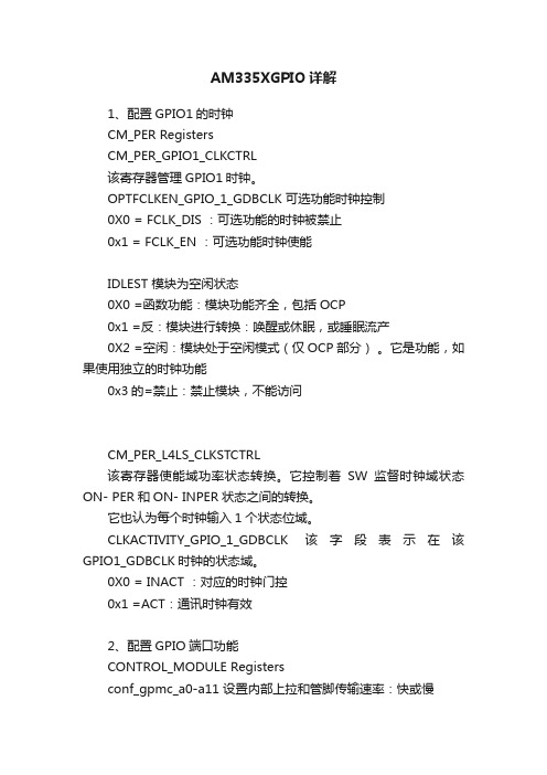
AM335XGPIO详解1、配置GPIO1的时钟CM_PER RegistersCM_PER_GPIO1_CLKCTRL该寄存器管理GPIO1时钟。
OPTFCLKEN_GPIO_1_GDBCLK 可选功能时钟控制0X0 = FCLK_DIS :可选功能的时钟被禁止0x1 = FCLK_EN :可选功能时钟使能IDLEST 模块为空闲状态0X0 =函数功能:模块功能齐全,包括OCP0x1 =反:模块进行转换:唤醒或休眠,或睡眠流产0X2 =空闲:模块处于空闲模式(仅OCP部分)。
它是功能,如果使用独立的时钟功能0x3的=禁止:禁止模块,不能访问CM_PER_L4LS_CLKSTCTRL该寄存器使能域功率状态转换。
它控制着SW监督时钟域状态ON- PER和ON- INPER状态之间的转换。
它也认为每个时钟输入1个状态位域。
CLKACTIVITY_GPIO_1_GDBCLK 该字段表示在该GPIO1_GDBCLK时钟的状态域。
0X0 = INACT :对应的时钟门控0x1 =ACT:通讯时钟有效2、配置GPIO端口功能CONTROL_MODULE Registersconf_gpmc_a0-a11 设置内部上拉和管脚传输速率:快或慢3、重启GPIO模块GPIO_SYSCONFIG 寄存器1 SOFTRESET R/W Software reset.This bit is automatically reset by the hardware. During reads, it always returns 0.0x0 = Normal mode0x1 = The module is rese软件复位。
该位由硬件自动复位。
在读取时,它总是返回0 。
0X0 =普通模式为0x1 =该模块复位4、设置GPIO方向GPIO_OE[0-31] 寄存器输出数据使能0X0 =相应的GPIO端口被配置为输出。
0x1 =相应的GPIO端口配置为输入。
电源管理芯片引脚定义

电源管理芯片引脚界说之老阳三干创作
1、 VCC 电源管理芯片供电
2、 VDD 门驱动器供电电压输入或低级控制信号供电源
3、VID-4 CPU与CPU供电管理芯片VID信号连接引脚, 主要指示
芯片的输出信号, 使两个场管输出正确的工作电压.
4、RUN SD SHDN EN 分歧芯片的开始工作引脚.
5、PGOOD PG cpu内核供电电路正常工作信号输出.
6、VTTGOOD cpu外核供电正常信号输出.
7、UGATE 高端场管的控制信号.
8、LGATE 低端场管的控制信号.
9、PHASE 相电压引脚连接过压呵护端.
10、VSEN 电压检测引脚.
11、FB 电流反馈输入即检测电流输出的年夜小.
12、COMP 电流赔偿控制引脚.
13、DRIVE cpu外核场管驱动信号输出.
14、OCSET 12v供电电路过流呵护输入端.
15、BOOT 次级驱动信号器过流呵护输入端.
16、VIN cpu外核...
CC:C=circuit 暗示电路的意思, 即接入电路的电压;。
am335x,GPIO学习
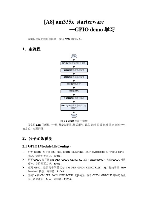
[A8] am335x_starterware—GPIO demo学习本例程实现功能比较简单,实现LED灯的闪烁。
1、主流程图1-1 GPIO程序主流程像常见LED闪烁程序一样,都是先配置,然后采取:置高-延时-拉低-延时-置高-延时……的方式,实现闪烁。
2、各子函数说明2.1 GPIO1ModuleClkConfig()配置GPIO1寄存器CM_PER_GPIO1_CLKCTRL(或上0x00000002),使能该GPIO1模块。
等待配置完毕。
P1049。
配置GPIO1寄存器CM_PER_GPIO1_CLKCTRL(或上0x00040000),使能GPIO1模块时钟。
等待配置完毕。
P1049。
检测GPIO1是否处于闲置状态CM_PER_GPIO1_CLKCTRL[17-16],若处于非fully functional状态,则等待。
P1049。
检测L4的CM_PER_L4LS_CLKSTCTRL的[19]位,查看GPIO1_GDBCLK时钟是否激活。
若未激活(Inact)则等待。
P1020。
2.2 GPIO1Pin23PinMuxSetup()GPIO1Pin23PinMuxSetup()配置GPMC_A7(GPIO1_23)引脚,配置为高速、下拉并使能。
Register=0x00000007。
p1278。
功能服用配置位为该寄存器[2:0],配置为111b,还未搞清楚。
2.3 GPIOModuleEnable()GPIOModuleEnable(GPIO_INSTANCE_ADDRESS)配置GPIO1时钟使能,GPIO_CTRL。
GPIO_CTRL[0]=0,使能GPIO1模块。
P4524。
2.4 GPIOModuleReset()GPIOModuleReset(GPIO_INSTANCE_ADDRESS)复位GPIO1各端口。
GPIO_SYSCONFIG。
GPIO_SYSCONFIG[1]=1,软件写1复位,复位GPIO1各端口。
AM335x IBIS Model使用指南说明书

How to use the AM335x IBIS ModelsIntroductionThe AM335x External Memory Interface is a very flexible interface which can be used with LPDDR, DDR2, DDR3, and DDR3L. There are many settings available to fine-tune the signal timing on this interface. These settings include ODT options, pullups, pulldowns, slew rate, etc. IBIS modeling can be used to fine tune the set of options for a given PCB. That said, understanding the mapping between the various IBIS models and the corresponding register configuration options is critical to doing this correctly. This article is intended to help bridge that gap so that AM335x users can properly model their memory interface and program the best options in the AM335x registers. NOTE: TI does not support timing analysis with IBIS simulations. Rather, customers are encouraged to use the IBIS models for Signal Integrity (SI) analysis. As far as the timing goes, please follow the routing guidelines and length/skew matching requirements in the Data Manual.IBIS StructureEvery pin on the device is listed with a corresponding "Selector". For example:P1 DDR_DQS0 Selector_1If you then go and look at the definition of that Selector you will find all of the available models for that given I/O cell. For example:[Model Selector] Selector_1Model_1000 INPUT,1.5V,FULLTERM, 1.00*RExt,IND,5%,DIFF_VREF_FULLTERM_8MA_5PER_1P5 Model_1001 INPUT,1.5V,Half Thevenin, 1.60*RExt,IND,5%,DIFF_VREF_HALFTERM_5MA_5PER Model_1002 INPUT,1.5V,FULLTERM, 0.88*RExt,IND,5%,DIFF_VREF_FULLTERM_9MA_5PER_1P5Each of the models above corresponds to the I/O cell behavior given a specific set of configuration options. Register MappingParameters for a typical modelEach model has the following structure:ReadsModel_xyz INPUT, <voltage>, <ODT>, <Impedance>, <Temperature>, <Voltage-tolerance> WritesModel_xyz 3-STATE, <voltage>, <ODT>, <slew>, <Impedance>, <Temperature>, <Voltage-tolerance>Parameter Options Register Setting TRM Reference<voltage>DDR3L (1.35V), DDR3 (1.5V), orDDR2/LPDDR (1.8V)<ODT>Reads:NOTERM_WEAK_PU_ON,NOTERM_WEAK_PD_ON,NOTERM_WEAK_PUPD_OFF,FULLTERM, Half TheveninWrites: ODT Off DDR_PHY_CTRL_1[reg_phy_rd_local_odt]Table 7-254.DDR_PHY_CTRL_1Register FieldDescriptions<slew>fastest, fast, slow, slowest ddr_cmd0_ioctrl, ddr_cmd1_ioctrl,ddr_cmd2_ioctrl, ddr_data0_ioctrl,ddr_data1_ioctrl ["sr" fields]Table 9-7. DDR Slew Rate Control Settings<Impedance>0.67*RExt0.73*RExt0.8*RExt0.88*RExt1.00*RExt1.14*RExt1.33*RExt1.6*RExt ddr_cmd0_ioctrl, ddr_cmd1_ioctrl,ddr_cmd2_ioctrl, ddr_data0_ioctrl,ddr_data1_ioctrl ["I" fields]Table 9-8. DDRImpedance ControlSettings<Temperature>IND = -40 to 125C, 25C nominal(In IBIS Comments)<Voltage-tolerance>(Power supply tolerance, not a register)5% or 10%Additional considerations for LPDDR vs DDR2LPDDR and DDR2 are both 1.8V interfaces. However, they use different signaling technologies:•LPDDR -> LVCMOS•DDR2 -> SSTLLet’s look at the pin DDR_D4 as an example…N3 DDR_D4 Selector_11So here is the corresponding snippet from Selector_11:|*****************************************************************************************| Usage I/O#1.35/1.5V/1.8V#X#X#BCSHTLTCSCDVPBFZ_SSDHV.PAD| Base model BCSHTLTCSCDVPBFZ_SSDHV|***************************************************************************************** [Model Selector] Selector_11<snip>Model_440 INPUT,1.8V,Pull-up/down off,IND,5%,VREF_NOTERM_PUPD_OFF_5PER_1P8<snip>Model_452 INPUT,1.8V,Pull-up/down off,IND,5%,LVCMOS_PUPD_OFF_5PER_1P8Model_440 and Model_452 above are nearly identical, but that is because both LPDDR and DDR2 are 1.8V interfaces. The final field holds the difference between them. Model_440 is of type VREF_NOTERM which3corresponds to DDR2 with no termination enabled (i.e. SSTL). Model_452 is of type LVCMOS, which is used for LPDDR.The register mapping that corresponds to this selection in the actual hardware is ddr_io_ctrl[mddr_sel]:•mddr_sel=0 -> DDR2/3 (SSTL)•mddr_sel=1 -> LPDDR (LVCMOS)Additional Notes on ioctrl Pin MappingThe ioctrl registers map to the actual pins as follows:Register[bits]Signalsddr_cmd0_ioctrl[9:5]ddr_ck, ddr_cknddr_cmd0_ioctrl[4:0]ddr_ba0, ddr_ba2, ddr_wen, ddr_a[9:8], ddr_a[6:3]ddr_cmd1_ioctrl[4:0]ddr_15, ddr_a[12:10], ddr_a7, ddr_a2, ddr_a0, ddr_ba1, ddr_casn, ddr_rasnddr_cmd2_ioctrl[4:0]ddr_cke, ddr_resetn, ddr_odt, ddr_csn0, ddr_[a14:13], ddr_a1ddr_data0_ioctrl[9:5]ddr_dqs1, ddr_dqsn1ddr_data0_ioctrl[4:0]ddr_d[15:8], ddr_dqm1ddr_data1_ioctrl[9:5]ddr_dqs0, ddr_dqsn0ddr_data1_ioctrl[4:0]ddr_d[7:0], dqm0ExampleIn AM335x EMIF Configuration tips the recommendation is to set all the IOCTRL registers to a value of 0x18B which breaks down as:•SR[9:8] = 01 slow•I[7:5] = 100 0.88*RExt•SR[4:3] = 01 slow•I[2:0] = 011 1.00*RExtAs an example, let's assume you would like to model this type of configuration for your own hardware. And let's assume for this example that you're using DDR3 (1.5V). Finally, we'll do this modeling using 5% power supply tolerance, though it could similarly be modeled using 10% tolerance (i.e. just choose the corresponding model).The IOCTRL settings above correspond to the slew rate for ALL signals being set to "slow". The Impedance is being configured differently for some of the signals. The breakdown of signals controlled by these registers can be found in Table 9-9. DDR PHY to IO Pin Mapping. The register descriptions of the IOCTRL specifies which signals are affected by SR[9:8]/I[7:5]. So in particular, the following use 0.88*RExt:•DQS•DQSn•CK•CKnCorrespondingly the signals above should choose models with Impedance of 0.88*RExt. The others should use1.00*RExt. So in this scenario we would use the following:4Signal Model DescriptionDQS Model_6553-STATE,1.5V,ODT off,slow, 0.88*RExt,IND,5%,SR01_9MA_PADP_5PER_1P5DQS#Model_8473-STATE,1.5V,ODT off,slow, 0.88*RExt,IND,5%,SR01_9MA_PADN_5PER_1P5CK Model_3433-STATE,1.5V,ODT off,slow, 0.88*RExt,IND,5%,SR01_9MA_5PER_1P5CK#Model_3433-STATE,1.5V,ODT off,slow, 0.88*RExt,IND,5%,SR01_9MA_5PER_1P5DQ Model_3523-STATE,1.5V,ODT off,slow, 1.00*RExt,IND,5%,SR01_8MA_5PER_1P5DM Model_3523-STATE,1.5V,ODT off,slow, 1.00*RExt,IND,5%,SR01_8MA_5PER_1P5Note that the write models always have ODT off since in that scenario ODT would be a function of the memory onthe other side. For reads, ODT would be the responsibility of AM335x and so that parameter is configurable for reads:Signal Model DescriptionDQS Model_1002INPUT,1.5V,FULLTERM, 0.88*RExt,IND,5%,DIFF_VREF_FULLTERM_9MA_5PER_1P5DQS#Model_1002INPUT,1.5V,FULLTERM, 0.88*RExt,IND,5%,DIFF_VREF_FULLTERM_9MA_5PER_1P5CK Model_3433-STATE,1.5V,ODT off,slow, 0.88*RExt,IND,5%,SR01_9MA_5PER_1P5CK#Model_3433-STATE,1.5V,ODT off,slow, 0.88*RExt,IND,5%,SR01_9MA_5PER_1P5DQ Model_496INPUT,1.5V,FULLTERM, 1.00*RExt,IND,5%,VREF_FULLTERM_8MA_5PER_1P5DM Model_3523-STATE,1.5V,ODT off,slow, 1.00*RExt,IND,5%,SR01_8MA_5PER_1P5Note that the DDR_CK, DDR_CKN, and DDR_DQM pins are always driven by the AM335x (not the memory) which is why it is of type "3-STATE" (output) for both write and read operations above.Verifying DDR ConfigurationAfter investing the effort to determine the best models for your board, it will be up to the software team to actually make the necessary changes. This final and most critical step of the process is often done improperly! In order to simplify the process, a JTAG based script was created to read important registers on the device and parse the contents to show what's actually being used. Here's how to use download and use this script:1.Download am335x-ddr-analysis.dss [1].unch CCS.3.Create an appropriate target configuration file for connecting to your board.•File -> New -> Target Configuration File•Supply a name/location for the file.•View -> Target Configurations to see the available target configurations (yours should now be among them!).•Double-click your file in the Target Configurations panel to open it for editing.•Select your emulator and processor. Be sure to select a processor and not a board, as we don't want any gel files to be part of the configuration. Save.unch the debugger, but do not connect to any CPUs.•In the Target Configurations window, right-click on your ccxml file and select "Launch Selected Configuration"unch the scripting console by going to View -> Scripting Console.6.Load am335x-ddr-analysis.dss in the scripting console by executing "loadJSFile<path-to-dss-file>/am335x-ddr-analysis.dss".57.It will use the Debug Access Port (DAP) unobtrusively behind the scenes such that the Cortex A8 is never halted.It will generate a am335x-ddr-analysis_yyyy-mm-dd_hhmmss.txt file on your desktop.References[1]https:///sitara-dss-files/am335x-dss-files/blobs/raw/master/am335x-ddr-analysis.dss6 Article Sources and ContributorsHow to use the AM335x IBIS Models Source: /index.php?oldid=235642 Contributors: BradGriffis。
关于AM335系列的板卡和相关模块产品常见问题
关于AM335系列的板卡和相关模块产品常见问题最近有客户在使用OK335x系列开发板中遇到了一些问题,所以在这里简单地总结了几点常见问题和解决方案,在这里分享一下。
如果您手中正好有飞凌的AM335x系列板卡,请仔细阅读,可能目前困扰您的问题答案就在这里!一.关于OK335x系列开发板,启动时,调试串口循环打印CCCCC问题分析以下为打印信息:建议从两方面进行问题排查:(1)OK335x系列开发板启动方式有2种:SD卡、nand. 请检查是否设置的SD卡启动,但是没有插SD卡或者SD卡中无程序。
底板上的拨码开关要拨到相应位置,参考以下说明:1. SD 卡启动设置:直接拨到 On2. NandFlash 启动设置:直接拨到 Off注:On 代表拨到上方,Off 代表拨到下方(2)飞凌OK335x系列开发板DI8-13的引脚,是boot启动项相关引脚。
如果您这几个引脚上接的外设模块电平跟uboot(下拉)启动电平相反,也可能会影响启动。
可以排查下是否是这几个引脚导致。
(3)如果排查以上两点还未解决问题,请联系飞凌技术支持************!二.关于OK335x系列开发板启动时,串口打印信息出现:please contact forlinx问题分析。
以下为打印信息:建议从两方面进行问题排查:(1)FET335x系列核心板上有个加密芯片:DS2406,通过IIC 接的CPU,这个芯片用户不能使用,因为出厂时里面已经写入了飞凌的加密信息,只有飞凌系统可以使用。
uboot在启动过程中会取读取保存在DS2460里的密码。
验证不通过的时候,会在串口打印信息里提示“Contact Forlinx….”,这种情况一般是加密芯片里的密码丢了,也可能是出厂没有烧写加密芯片。
(2)除了加密芯片用了一路IIC接口,核心板还支持2路,有些用户需要接自己的IIC外设模块。
如果您把设备挂载到加密芯片的这路IIC上,地址出现冲突,这样也可能会有影响,出现“please contact forlinx”信息。
03 AM335x处理器
北京交通大学
国家电工电子教学基地
Introduction to AM335x
AM335X 系列处理器
• 不同配置,引脚兼容
北京交通大学
国家电工电子教学基地
AM335x Processor
基于AM335x处理器的硬件系统
• AM335x介绍 • 主处理器
• 片上模块
• 硬件构成要点
• 开发资源
北京交通大学
国家电工电子教学基地
Main processor
存储器映射 (L3)
• GPMC (外接存储器)
– 0x0000_0000- 0x1FFF_FFFF, 512MB 8-/16-bit External Memory (ex/r/w)
• Boot ROM
– 0x4002_0000 0x4002_BFFF 48KB, (32b, ex/r)
北京交通大学 国家电工电子教学基地
Main processor
存储器子系统: EMIF
• 16-bit data width
• support DDR2/DDR3/mDDR • On-chip 128-bit interface
Cmd/addr 128-bit OCP DDR2/3/ mDDR Memory Controller DDR data
• 可应用于家庭自动化,工业自动化,工业平板,便携导 航设备和网络互联。
北京交通大学 国家电工电子教学基地
Introduction to AM335x
AM335X 功能模块
• 3个子系统
– A8 MPU 子系统 – POWERVR SGX 图形加速子系统 – PRU-ICSS 实时单元和工业 通信子系统
am335x双网络工控板原理图

B
GPIO0_26 GPIO0_27 GPIO0_28 GPIO0_29 GPIO0_30 GPIO0_31
B
A
深圳市盈鹏飞科技有限公司 设计 Bills 日期 2015.03.11 日期 Date 校对 Leo 审核 Ping 日期 Date 批准 Ping 日期 Date
Friday, September 04, 2015
名称 编号 说明 版本 页码 工业单板电脑 EVB-335X-II REVISION HISTORY V1.00 第 5 页 共 23 页
1 A
5
4
3
2
1
01 - CoM-335X STAMP CHIP 03 - RMII ETHERNET RMII_MDC RMII_MDIO SPI0_CLK SPI0_MISO SPI0_MOSI SPI0_CS0 AM33_INT0 SYS_NRST GPIO0_16 GPIO0_17
1 A
5
4
3
2
1
D
D
PIO MUX
GPIO0 GPIO0_0 GPIO0_1 GPIO0_2 GPIO0_3 GPIO0_4 GPIO0_5 GPIO0_6 GPIO0_7 GPIO0_8 GPIO0_9 GPIO0_10 GPIO0_11 GPIO0_12 GPIO0_13 GPIO0_14 GPIO0_15 GPIO0_16 GPIO0_17 GPIO0_18 GPIO0_19 GPIO0_20 GPIO0_21 GPIO0_22 GPIO0_23 GPIO1 GPIO1_0 GPIO1_1 GPIO1_2 GPIO1_3 GPIO1_4 GPIO1_5 GPIO1_6 GPIO1_7 GPIO1_8 LCD_D12 GPIO1_9 LCD_D13 GPIO1_10 LCD_D14 GPIO1_11 LCD_D15 GPIO1_12 I2C2_SDA GPIO1_13 I2C2_SCL GPIO1_14 UART1_RXD GPIO1_15 UART1_TXD GPIO1_16 CAN0_TX(RTC_SDA) GPIO1_17 CAN0_RX(RTC_SCL) GPIO1_18 USB0_DRVVBUS GPIO1_19 XDMA_INTR0 GPIO1_20 XDMA_INTR1 GPIO1_21 RMII1_TXD1 GPIO1_22 GPMC_D8 GPIO1_23 GPMC_D9 GPIO1_24 GPIO1_25 GPIO1_26 GPMC_D10 GPIO1_27 GPMC_D11 GPIO1_28 RMII1_TXD0 GPIO1_29 RMII1_REFCLK GPIO1_30 GPMC_WAIT0(rmii2_crs_dv) GPIO1_31 GPMC_WPn USAGE MDIO MDC SPI0_CLK SPI0_MISO SPI0_MOSI SPI0_CS0 MMC0_POW USAGE GPMC_D0(MMC1_D0) GPMC_D1(MMC1_D1) GPMC_D2(MMC1_D2) GPMC_D3(MMC1_D3) GPMC_D4(MMC1_D4) GPMC_D5(MMC1_D5) GPMC_D6(MMC1_D6) GPMC_D7(MMC1_D7) I2C1_SDA(UART4_RXD) I2C1_SCL(UART4_TXD) UART0_RXD UART0_TXD GPMC_D12 GPMC_D13 GPMC_D14 GPMC_D15 GPMC_A0(rmii2_txen) GPMC_A1 GPMC_A2 GPMC_A3 GPMC_A4(rmii2_txd1) GPMC_A5(rmii2_txd0) GPMC_A6 GPMC_A7 GPMC_A8 GPMC_A9 GPMC_A10(rmii2_rxd1) GPMC_A11(rmii2_rxd0) GPMC_BEn1 GPMC_CSn0 GPMC_CSn1(MMC1_CLK) GPMC_CSn2(MMC1_CMD) GPIO2 GPIO2_0 GPIO2_1 GPIO2_2 GPIO2_3 GPIO2_4 GPIO2_5 GPIO2_6 GPIO2_7 GPIO2_8 GPIO2_9 GPIO2_10 GPIO2_11 GPIO2_12 GPIO2_13 GPIO2_14 GPIO2_15 GPIO2_16 GPIO2_17 GPIO2_18 GPIO2_19 GPIO2_20 GPIO2_21 GPIO2_22 GPIO2_23 GPIO2_24 GPIO2_25 GPIO2_26 GPIO2_27 GPIO2_28 GPIO2_29 GPIO2_30 GPIO2_31 USAGE GPMC_CSn3 GPMC_CLK GPMC_ALE GPMC_RE GPMC_WE GPMC_CLE LCD_D0 LCD_D1 LCD_D2 LCD_D3 LCD_D4 LCD_D5 LCD_D6 LCD_D7 LCD_D8 LCD_D9 LCD_D10 LCD_D11 UART3_RXD UART3_TXD RMII1_RXD1 RMII1_RXD0 LCD_VS LCD_HS LCD_CLK LCD_DE MMC0_D3 MMC0_D2 MMC0_D1 MMC0_D0 MMC0_CLK MMC0_CMD GPIO3 GPIO3_0 GPIO3_1 GPIO3_2 GPIO3_3 GPIO3_4 GPIO3_5 GPIO3_6 GPIO3_7 GPIO3_8 GPIO3_9 GPIO3_10 USAGE RMII2_REFCLK RMII1_CRS_DV RMII1_RXERR RMII1_TXEN GPIO_BUZZ I2C0_SDA I2C0_SCL USER LED(RUN) CRYPTO UART2_RXD UART2_TXD
- 1、下载文档前请自行甄别文档内容的完整性,平台不提供额外的编辑、内容补充、找答案等附加服务。
- 2、"仅部分预览"的文档,不可在线预览部分如存在完整性等问题,可反馈申请退款(可完整预览的文档不适用该条件!)。
- 3、如文档侵犯您的权益,请联系客服反馈,我们会尽快为您处理(人工客服工作时间:9:00-18:30)。
管脚具体说明 电源地 电源地 RTC电源 USB1电源输出控制 USB0电源输出控制 USB0差分数据 USB0差分数据 USB0 OTG ID I2C0时钟 S时钟 串口5数据接收 串口2数据接收 串口4数据接收 串口0数据接收 串口1数据接收 串口3数据接收 CAN0接收数据 eRPWM0 B输出 I2C1数据 SPI1数据 SPI1片选 复位 电源地 模拟量输入 模拟量输入 模拟量输入 ADC地 推荐功能(底板使用) 电源地 电源地 RTC电源 USB1 USB0 USB0 USB0 USB1 I2C0 SD0卡信号 SD0卡信号 SD0卡信号 AUDIO 串口5 串口2 串口4 串口0 串口1 串口3 CAN0 eRPWM0 I2C1 SPI1 SPI1 复位 电源地 ADC ADC ADC ADC地 功能 电源地 电源地 RTC电源 USB1_DRVVBUS USB0_DRVVBUS USB0_DM USB0_DP USB1_ID I2C0_SCL MMC0_CLK MMC0_DAT0 MMC0_DAT2 GPIO3_21 UART5_RX UART2_RX UART4_RX UART0_RX UART1_RX UART3_RX DCAN0_RX eHRPWM0B 2C1_SDA SPI1_D0 SPI1_CS0 nRESETIN_OUT 电源地 AIN5 AIN3 AIN1 ADC地 IO管脚 DGND DGND VDD18_EXT_RTC F15 F16 N18 N17 P17 C16 G17 G16 F18 A14 H16 H17 E18 E15 D16 C15 D17 B17 B16 B13 C12 A10 DGND B8 A7 C7 GNDA_ADC 管脚 管脚 1 3 5 7 9 11 13 15 17 19 21 23 25 27 29 31 33 35 37 39 41 43 45 47 49 51 53 55 57 59 2 4 6 8 10 12 14 16 18 20 22 24 26 28 30 32 34 36 38 40 42 44 46 48 50 52 54 56 58 60 IO管脚 +3V3 +3V3 T18 P15 R18 R17 P16 C17 DGND G18 G15 F17 H18 J15 E17 E16 D15 C18 D18 A17 A16 A13 D12 D13 B18 A8 C8 B7 B6 VDD_ADC 功能 3V3电源 3V3电源 USB1_VBUS USB0_VBUS USB1_DM USB1_DP USB0_ID I2C0_SDA 电源地 MMC0_CMD MMC0_DAT1 MMC0_DAT3 UART5_TX UART2_TX UART4_TX UART0_TX UART1_TX UART3_TX DCAN0_TX eHRPWM0A I2C1_SCL SPI1_SCLK SPI1_D1 GPIO3_20 nNMI AIN6 AIN4 AIN2 AIN0 ADC电源 推荐功能(底板使用) 电源 电源 USB1 USB0 USB1 USB1 USB0 I2C0 电源地 SD0卡信号 SD0卡信号 SD0卡信号 串口5 串口2 串口4 串口0 串口1 串口3 CAN0 eRPWM0 I2C1 SPI1 SPI1 GPIO 外部中断 ADC ADC ADC ADC ADC电源 管脚具体说明 核心板3V3电源供电 核心板3V3电源供电 USB1电源 USB0电源 USB1差分数据 USB1差分数据 USB0 OTG ID I2C0数据 电源地 SD0卡控制信号 SD0卡数据 SD0卡数据 串口5数据发送 串口2数据发送 串口4数据发送 串口0数据发送 串口1数据发送 串口3数据发送 CAN0发送数据 eRPWM0 A输出 I2C1时钟 SPI1时钟 SPI1数据 AUDIO I2S 数据输入 外部中断输入信号 模拟量输入 模拟量输入 模拟量输入 模拟量输入 ADC电源
LCD_DATA7 T4 LCD_DATA5 T2 LCD_DATA3 R4 LCD_DATA1 R2 电源地 DGND RGMII1_TRN3 RGMII1_TRN3 RGMII1_TRN2 RGMII1_TRN2 RGMII1_TRN1 RGMII1_TRN1 RGMII1_TRN0 RGMII1_TRN0 RGMII1_LED_LINK RGMII1_LED_LINK
MYC-AM335X核心板CN2引脚定义表
管脚具体说明 管理数据输入输出信号 网口接收数据 网口接收数据 网口接收时钟 网口发送数据 网口发送数据 网口接收控制信号 电源地 WIFI时钟 WIFI数据 WIFI数据 LED控制信号 BlueTooth启动 电源地 LCD使能 LCD 垂直同步信号 LCD数据线(红) LCD数据线(红) LCD数据线(红) LCD数据线(绿) LCD数据线(绿) LCD数据线(绿) LCD数据线(蓝) LCD数据线(蓝) 电源地 网口差分数据 网口差分数据 网口差分数据 网口差分数据 网络链接指示灯 推荐功能(底板使用) 网口2 网口2 网口2 网口2 网口2 网口2 网口2 电源地 WIFI WIFI WIFI GPIO BLUETOOTH 电源地 LCD LCD LCD LCD LCD LCD LCD LCD LCD LCD 电源地 网口1 网口1 网口1 网口1 网口1 功能 MDIO_DATA RGMII2_RD0 RGMII2_RD2 RGMII2_RCLK RGMII2_TD0 RGMII2_TD2 RGMII2_RCTL 电源地 MMC2_CLK MMC2_DAT3 MMC2_DAT1 MMC2_DAT7 MMC2_DAT5 电源地 LCD_AC_BIAS_EN LCD_VSYNC LCD_DATA15 LCD_DATA13 LCD_DATA11 LCD_DATA9 IO管脚 M17 V17 U16 T15 V15 T14 V14 DGND V12 U13 R12 U12 T10 DGND R6 U5 T5 V3 U4 U2 管脚 管脚 1 3 5 7 9 11 13 15 17 19 21 23 25 27 29 31 33 35 37 39 41 43 45 47 49 51 53 55 57 59 2 4 6 8 10 12 14 16 18 20 22 24 26 28 30 32 34 36 38 40 42 44 46 48 50 52 54 56 58 60 IO管脚 M18 T16 V16 U15 R14 U14 R13 DGND T13 V13 T12 T11 U10 3 R5 V5 V4 V2 U3 U1 T3 T1 R3 R1 DGND RGMII1_TRP3 RGMII1_TRP2 RGMII1_TRP1 RGMII1_TRP0 RGMII1_LED_ACT 功能 MDIO_CLK RGMII2_RD1 RGMII2_RD3 RGMII2_TCLK RGMII2_TD1 RGMII2_TD3 RGMII2_TCTL 电源地 MMC2_CMD MMC2_DAT2 MMC2_DAT0 MMC2_DAT6 MMC2_DAT4 电源地 LCD_HSYNC LCD_PCLK LCD_DATA14 LCD_DATA12 LCD_DATA10 LCD_DATA8 LCD_DATA6 LCD_DATA4 LCD_DATA2 LCD_DATA0 电源地 RGMII1_TRP3 RGMII1_TRP2 RGMII1_TRP1 RGMII1_TRP0 RGMII1_LED_ACT 推荐功能(底板使用) 网口2 网口2 网口2 网口2 网口2 网口2 网口2 电源地 WIFI WIFI WIFI WIFI WIFI 电源地 LCD LCD LCD LCD LCD LCD LCD LCD LCD LCD 电源地 网口2 网口2 网口2 网口2 网口2 管脚具体说明 管理数据时钟信号 网口接收数据 网口接收数据 网口发送时钟 网口发送数据 网口发送数据 网口发送控制信号 电源地 WIFI控制信号 WIFI数据 WIFI数据 WIFI中断请求 WIFI启动 电源地 LCD 水平同步信号 LCD像素时钟 LCD数据线(红) LCD数据线(红) LCD数据线(绿) LCD数据线(绿) LCD数据线(绿) LCD数据线(蓝) LCD数据线(蓝) LCD数据线(蓝) 电源地 网口差分数据 网口差分数据 网口差分数据 网口差分数据 网络传送指示灯