Practical Power Analysis Attacks to RSA on a Large IP Portfolio SoC
英语演讲与辩论课件Lecture Two

Language Use in Debate
• Precision Vocabulary: Use accurate and specific vocabulary to express one's views and positions, avoiding the use of vague and vague words.
• Clear Expression: Maintain fluent and clear language, allowing the other party and audience to accurately understand their own viewpoints and arguments.
要点二
Addressing the challenges of globalization
With the accelerated development of globalization, English speaking and debating skills have become important skills for international communication and cooperation. This course aims to help students adapt to the challenges of globalization and enhance their international competitiveness.
Opening statement
Attract the audience's attention, establish a connection with them, and lay a solid foundation for the speech.
A low-noise, low-power VCO
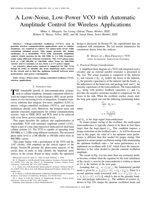
A Low-Noise,Low-Power VCO with AutomaticAmplitude Control for Wireless ApplicationsMihai A.Margarit,Joo Leong(Julian)Tham,Member,IEEE,Robert G.Meyer,Fellow,IEEE,and M.Jamal Deen,Senior Member,IEEE Abstract—Voltage-controlled oscillators(VCO’s)used inportable wireless communications applications,such as cellulartelephony,are required to achieve low phase-noise levels whileconsuming minimal power.This paper presents the designchallenges of a monolithic VCO with automatic amplitudecontrol,which operates in the300MHz to1.2GHz frequencyrange using different external resonators.The VCO phase-noiselevel is0106dBc/Hz at100-KHz offset from an800-MHzcarrier,and it consumes1.6mA from a2.7-V power supply.An extensive phase-noise analysis is employed for this VCOdesign in order to identify the most important noise sourcesin the circuit and tofind the optimum tradeoff between noiseperformance and power consumption.Index Terms—Phase noise,voltage-controlled oscillator(VCO),wireless applications.I.I NTRODUCTIONT HE remarkable growth in telecommunication systems,such as cellular telephony,demands continuous efforts to-ward the improvement of radio-frequency(RF)circuit perfor-mance at ever increasing levels of plete trans-ceiver solutions that integrate low-noise amplifiers(LNA’s),mixers,voltage-controlled oscillators(VCO’s),and transmitmodulators already exist.Moreover,the stringent noise andspurious emissions requirements for cellular communicationssystems,such as GSM,DCS,and PCS,need to be achievedwith even lower power-consumption levels.This paper describes the analysis and implementation ofa monolithic VCO with automatic amplitude control(AAC),which is part of a one-chip transceiver dedicated for dual-bandcellular systems[1].The VCO is capable of operating from300MHz to1.2GHz using different resonators.The measuredphase-noise level is(a)(b)Fig.1.(a)Simplified diagram of a voltage-controlled oscillator.(b)V oltage-controlled oscillator with damping resistor R s:has negligible effect on the fundamental mode[2].However,care needs to be taken in the design,since too large a valueoffor the differential amplifier in order to maintain constantMARGARIT et al.:LOW-NOISE,LOW-POWER VCO763Fig.2.Schematic of the VCO with AAC.gain.for minimum phase-noise levels largely independent of considerations for proper oscillation startup. In steady-state operation,the AAC loop forces the dc signal provided by the rectifier and the low-passfilter at the sensing input to track the reference level applied at the reference input.This leads to the second advantage of using the AAC circuit of enabling the VCO to provide constant output power independent of theresonator(3)Since the system is timevariant,and observation timein(3)with theequivalent noise source of each individual node,the phase-noise contribution of each node can be calculated[5].To explore the oscillator excess phase response,each nodeof the circuit needs to be excited at evenly distributed timesteps of the oscillation period.Due to thehighis an integer chosen such that the oscillation waveform hassettled before the next pulse is applied.The ramp generator isreset by thefirst positive-going zero crossing of the oscillation.The ramp is then compared in COMP2with a staircase voltage,which is incremented ateachis the number of pulses to be injected.In this way,pulses areinjected with a period equalto764IEEE JOURNAL OF SOLID-STATE CIRCUITS,VOL.34,NO.6,JUNE1999(a)(b)(c)Fig.3.(a)Sequence of pulses used to excite the oscillator.(b)Block diagram of the behavioral test generator.(c)VCO test points for phase sensitivity to injectedcharge.Fig.4.Impulse shape.is almost constant from DC to 25GHz,which is sufficient for this design that uses a bipolar processwithCurrentsourcethe effect of thenoise voltage generatedbytheeffect of the resistive losses in theresonator(5)(6)The collector shot noise oftransistormA).Thecyclostationarityofis8.6MARGARIT et al.:LOW-NOISE,LOW-POWER VCO765Fig.5.Tail-current noise spectrum.(a)(b)Fig.6.(a)VCO output waveform.(b)Simulated function h8;I(t; )(vertical axis in degrees/pC).across the nodes“out”and“outb”(Fig.2),and it has thevaluefor current pulsesinjected at the tail of the emitter-coupled pair.This functionhas a periodicity that is half the oscillation period.To obtainmore meaningful information on the phase sensitivity forperturbations in the tail current of the VCO,the functionis plotted together with the oscillation outputwaveform.It can be seen that for perturbations injectedaround the zero crossings and the peaks of the oscillation,the phase sensitivity is close to zero and reaches its maxima766IEEE JOURNAL OF SOLID-STATE CIRCUITS,VOL.34,NO.6,JUNE1999Fig.7.Frequency spectrum of h 8;I (t; )(vertical axis in dBV).forwhereis shown in Fig.7.As expected,there areharmonics at multiples of double the oscillation frequency.The harmonics mix with the noise around these frequencies and contribute to the total phase noise.For calculation of the phase-noise contribution from the tail current,the Fourier coefficientsof[4]th harmonic of the oscillation fre-quency.In this analysis,the summation is performed over the first five harmonics.Higher order harmonics have insignificant contribution to the phase noise.Of particular interest is the dc component,coefficientregion of the phase noiseintersectstheis definedas(9)In the aboveequation,andhas a period equalto the oscillation period.Again,in order to see the effect of this noise source,the oscillation output waveform and the collector currentofreaches its maximum when the collector currentis close to the peak,and it reaches the minimumwhenin Fig.9show that thecollector shot noise is mixed mostly with the first and second harmonics of the oscillation frequency to contribute to the total phase noise.However,the collector shot noiseofwas performed.Todo this,theratioMARGARIT et al.:LOW-NOISE,LOW-POWER VCO767(a)(b)(c)Fig.8.(a)VCO output waveform.(b)Collector current of Q1.(c)Simulated functions h8;IIt768IEEE JOURNAL OF SOLID-STATE CIRCUITS,VOL.34,NO.6,JUNE 1999Fig.9.Frequency spectrum of h 8e (t; )(vertical axis in dBV).Fig.10.Phase noise (continuous line)and figure of merit (dashed line)versus feedback ratio n:TABLE IN OISE C ONTRIBUTIONS AT100-kHz O FFSET FROM AN 800-MHz C ARRIERAlthough the noise contribution from the tail current is not important at this offset frequency,it becomes the major noise source at offset frequencies less than 3kHz.The factor of two for some of the noise sources in Table I accounts for noise sources that are considered twice due to the circuit symmetry [5].The sum of these values gives a noise-to-signal ratio ofregion of the spectrum.SpectreRFpredicts a phase-noise level ofMARGARIT et al.:LOW-NOISE,LOW-POWER VCO769parison of the phase noise calculated with phase noise simulated in SpectreRF.Fig.12.Microphotograph of the VCO with AAC.However,the current version of SpectreRF did not predictthe43dBc and the third harmonic is106dBc/Hz at100-770IEEE JOURNAL OF SOLID-STATE CIRCUITS,VOL.34,NO.6,JUNE1999Fig.13.VCO outputspectrum.Fig.14.Measured phase noise.kHz offset for a carrier frequency of 800MHz,which is in agreement with the analysis presented in this paper (Fig.14).The VCO core consumes 1.6mA from a 2.7-V power supply.The remaining circuits used for the AAC (rectifier,voltage reference,and amplifier)consume 0.25mA.If better phase-noise performance is desired,only the current consumption inthe VCO core needs to be increased,while the consumption of the AAC circuits remains unchanged.V.C ONCLUSIONSIn this paper,the possibilities of developing a low-noise,low-power VCO with capabilities for wireless applicationsMARGARIT et al.:LOW-NOISE,LOW-POWER VCO 771have been explored.An automatic amplitude control circuit was implemented,which allows the choice of the optimum oscillator feedback ratio for noise performance without being constrained by startup considerations.At the same time,the automatic amplitude control allows proper VCO operation for a wide range of the resonator quality factor.A novel method was used to study the phase-noise performance of the VCO.The method predicts results that are close to the measurements and allows the designer to obtain detailed information about the processes that contribute to oscillator phase noise.A CKNOWLEDGMENTThe authors would like to thank Dr.C.Hull and R.Magoon for helpful discussions.R EFERENCES[1]J.L.Tham,M.Margarit,B.Pregardier, C.Hull,and F.Carr,“A2.7V 900MHz/1.9GHz dual-band transceiver IC for digital wireless communication,”in Proc.CICC ,1998,p.559.[2]J.L.Tham,“Integrated radio frequency LC voltage-controlled oscil-lators,”College of Engineering,University of California,Berkeley,Electronics Research Laboratory Memo.,1995.[3]P.Davis,P.Smith,E.Campbell,J.Lin,K.Gross,G.Bath,Y.Low,M.Lau,Y.Degani,J.Gregus,R.Frye,and K.Tai,“Si-on-Si integration of a GSM transceiver with VCO resonator,”in Proc.ISSCC 1998,vol.41,Feb.1998,p.248.[4] A.Hajimiri and T.H.Lee,“A general theory of phase noise in electricaloscillators,”IEEE J.Solid-State Circuits ,vol.33,pp.179–194,Feb.1998.[5] C.D.Hull and R.G.Meyer,“A systematic approach to the analysisof noise in mixers,”IEEE Trans.Circuits Syst.I ,vol.40,pp.909–919,Dec.1993.Mihai A.Margarit received the Dipl.Ing.degree in electrical engineering from the “Politehnica”Uni-versity Bucharest,Romania,in 1984.He currently is pursuing the Ph.D.degree in electrical engineering at Simon Fraser University,Burnaby,B.C.,Canada.Since 1984,he has worked in analog circuit design for the National Institute for Microelectron-ics,Bucharest,the Fraunhofer Institute,Erlangen,Germany,and Simon Fraser University,Vancouver,Canada.He is currently with Rockwell Semicon-ductor Systems,Newport Beach,CA,where he isa Senior Design Engineer working on high-frequency circuits for wireless communicationapplications.Joo Leong (Julian)Tham (S’88–M’96)received the B.S.degree in electrical engineering (with high-est honors)from the University of California,Santa Barbara,and the M.S.degree in electrical engineer-ing from the University of California,Berkeley.He has worked at Raytheon and Trimble Navi-gation.His previous work includes autocalibration systems and global positioning system receivers.From 1993to 1999,he was with Rockwell Semi-conductor Systems,Newport Beach,CA,where he was a Principal Design Engineer and Managerworking on radio-frequency integrated circuits for wireless communication applications.He currently is with Maxim Integrated Products,Sunnyvale,CA.His current interests are in the areas of high-frequency circuit design and integrated transceiver architectures.Mr.Tham is a member of Eta Kappa Nu,Tau Beta Pi,and the Golden Key Honor Society.He was named Rockwell Semiconductor Systems Engineer of the Year in1995.Robert G.Meyer (S’64–M’68–SM’74–F’81)was born in Melbourne,Australia,on July 21,1942.He received the B.E.,M.Eng.Sci.,and Ph.D.degrees in electrical engineering from the University of Melbourne in 1963,1965,and 1968,respectively.In 1968,he was an Assistant Lecturer in electrical engineering at the University of Melbourne.Since September 1968,he has been with the Department of Electrical Engineering and Computer Sciences,University of California,Berkeley,where he is now a Professor.His current research interests are high-frequency analog integrated-circuit design and device fabrication.He has been a Consultant on electronic circuit design for numerous companies in the electronics industry.He is a coauthor of Analysis and Design of Analog Integrated Circuits (New York:Wiley,1993)and Editor of Integrated Circuit Operational Amplifiers (New York:IEEE Press,1978).Dr.Meyer was President of the IEEE Solid-State Circuits Council and was an Associate Editor of the IEEE J OURNAL OF S OLID -S TATE C IRCUITS and of the IEEE T RANSACTIONS ON C IRCUITS AND S YSTEMS.M.Jamal Deen (S’81–M’86–SM’92)was born in Georgetown,Guyana.He received the B.Sc.degree in physics and mathematics from the University of Guyana in 1978and the M.S.and Ph.D.degrees in electrical engineering and applied physics from Case Western Reserve University,Cleveland,OH,in 1982and 1985,respectively.From 1978to 1980,he was an Instructor of physics at the University of Guyana.From 1980to 1983,he was a Research Assistant at Case Western Reserve University.He was a Research Engineer(1983–1985)and an Assistant Professor (1985–1986)at Lehigh University,Bethlehem,PA.In 1986,he joined the School of Engineering Science,Simon Fraser University,Vancouver,BC,Canada,as an Assistant Professor and since 1993has been a full Professor.He was a Visiting Scientist at the Herzberg Institute of Astrophysics,National Research Council,Ottawa,Ont.,Canada,in summer 1986,and he spent his sabbatical leave as a Visiting Scientist at Northern Telecom,Ottawa,in 1992–1993.He was also a Guest Professor in the Faculty of Electrical Engineering,Delft University of Technology,The Netherlands,in summer 1997and a CNRS scientist at the Physics of Semiconductor Devices Laboratory,Grenoble,France,in summer 1998.His current research interests include integrated devices and circuits;device physics,modeling,and characterization;and low-power,low-noise,high-frequency circuits.Dr.Deen is a member of Eta Kappa Nu,the American Physical Society,and the Electrochemical Society.He was a Fulbright-Laspau Scholar from 1980to 1982,an American Vacuum Society Scholar from 1983to 1984,and an NSERC Senior Industrial Fellow in 1993.。
模幂算法的功耗攻击与双线性对密码算法的故障攻击分析

ABSTRACTCryptography is widely used in mobile internet, internet of things, finance, na-tional defense and other areas of information security. It makes high demands for the security of Cryptosystem. Public key cryptography is an important branch of cryptog-raphy and has been widely used in cryptography. With the emergence of side channel attack, hardware implementations of many algorithms are no longer safe. Therefore, the study of the security of the existing algorithms becomes very important. Increas-ing the defensive measures for the encryption products has become a problem that must be considered before designing. As the core operation of many classical public key cryptosystem, modular exponentiation algorithm has attracted much more atten-tion. At the same time, some new public key cryptosystems are also emerging. The academic research on the safety of these algorithms is still in its initial stage. Among them, the bilinear cryptographic algorithm has been widely studied because of its ex-cellent features and greater security.For modular exponentiation algorithm, this thesis studies the power analysis at-tack. Based on the N-1 attack, we proposed extended attacks. What’s more, we carried out experiment against ASIC implementation of two modular exponentiation algo-rithms. For the pairing algorithms, this thesis makes a study in fault attack and pre-sents a branch-based fault attack. We use Magma to prove the correctness of the at-tack. The work content and innovation of this thesis are as follows: (1) We made an in-depth study of the N-1 attack and proposed the extended N-1 attack. The values of x which meet the equation x2 mod n=1can be used by the chosen-message attack. With these values, we have successfully attacked Boscher's algorithm and Montgom-ery powering ladder. (2) The thesis has proposed countermeasures which can defense the extended N-1 attack. (3) This thesis proposed a branch-based fault attack against Miller loop of pairing algorithms which is suitable for all pairing algorithms that con-tain the Miller loop and has the advantage of possessing a variety of ways to inject faults. (4) Targeted preventive measures have been proposed. It will provide a refer-ence to the physical security of cryptographic systems.Key words:power analysis attack, N-1 attack, fault attack, modular exponentiation, bilinear pairing目录第一章绪论 (1)1.1 课题研究背景和意义 (1)1.2 模幂算法的功耗分析攻击研究现状 (2)1.3 双线性对密码算法的故障攻击研究现状 (3)1.4 论文的研究内容 (4)1.5 论文的章节安排 (5)第二章算法简介 (6)2.1 数论基础 (6)2.1.1 有限域算术 (6)2.1.2 椭圆曲线算术 (7)2.2 模幂算法 (7)2.2.1 Boscher的模幂算法 (9)2.2.2 蒙哥马利阶梯算法 (9)2.3 双线性对密码算法 (10)2.4 本章小结 (12)第三章旁路攻击 (13)3.1 功耗分析攻击 (13)3.1.1 CMOS电路的能量消耗 (13)3.1.2 能量碰撞介绍 (14)3.1.3 选择明文(N-1)攻击 (15)3.2 故障攻击 (17)3.3 本章小结 (18)第四章攻击与防御方法分析 (19)4.1 针对模幂算法的功耗攻击分析 (19)4.1.1 针对Boscher的模幂算法的功耗攻击分析 (19)4.1.2 针对蒙哥马利阶梯算法的功耗攻击分析 (21)4.2 针对模幂算法功耗攻击的防御措施 (24)4.2.1 Boscher的模幂算法的防御措施及算法改进 (24)4.2.2 蒙哥马利阶梯算法的防御措施 (24)4.3 针对双线性对密码算法的故障攻击分析 (25)4.3.1 故障注入点选择 (25)4.3.2 P为密钥点,Q为公共参数点 (26)4.3.3 Q为密钥点,P为公共参数点 (27)4.3.4 针对故障植入的讨论 (28)4.4 针对双线性对算法的防御措施 (28)4.5 本章小结 (29)第五章实验结果与分析 (31)5.1 针对模幂算法功耗攻击 (31)5.1.1 功耗信息的采集方式 (31)5.1.2 模幂算法的硬件实现 (32)5.1.3 针对Boscher的模幂算法的功耗攻击 (34)5.1.4 针对蒙哥马利阶梯算法的功耗攻击 (36)5.2 针对双线性对密码算法的故障攻击 (37)5.3 本章小结 (39)第六章总结与展望 (40)6.1 工作总结 (40)6.2 工作展望 (41)参考文献 (42)发表论文和参加科研情况说明 (45)致谢 (46)第一章绪论1.1课题研究背景和意义随着3G、4G移动互联网、物联网和云计算等新技术的迅猛发展,人类的生活正在变得越来越信息化、智能化。
TUG

Analysis of MO-1 (4)
Table 2: Conditional p(00|DD) = p(01|DD) = p(10|DD) = p(11|DD) = probabilities for “DD” and “ADAD” 1/2 p(00|ADAD) = 0 0 p(01|ADAD) = 1/4 1/4 p(10|ADAD) = 1/4 1/4 p(11|ADAD) = 1/2
P=P+Q
1
1 0 P=P+Q Q=4Q
P=P−Q Q=4Q 1
1
2
11 P=P+Q
0
0 0 Q=2Q P=P+Q Q=2Q 1 Q=2Q
M = 1 2 0 0 1 0 1 2 2 Figure 2: Transition matrix for FSM-MO-1
7
1 2
1 2
Figure 1: FSM-MO-1
DPA @ A-SIT/IAIK
DPA@IAIK
IAIK
Motivation (1)
TUG
• Recent paper of R¨ omer et. al. ”Information Leakage Attacks against Smart Card Implementations of the ECDSA” • They show how to calculate the secret key of the ECDSA by knowing some keybits of some ephemeral keys. • More precisely : At most 12 (consecutive) keybits, from about 50 ephemeral keys, for a 160-bit curve. • These are worst case bounds. • Extension of the attack is possible → arbitrary located keybits.
Fault Attacks on Dual-Rail Encoded Systems

Fault Attacks on Dual-Rail Encoded SystemsJason Waddle and David Wagner Department of Computer Science University of California, Berkeley jwaddle@, daw@AbstractFault induction attacks are a serious concern for designers of secure embedded systems. An ideal solution would be a generic circuit transformation that would produce circuits that are robust against fault induction attacks. We develop a framework for analyzing the security of systems against single fault attacks and apply it to a recent proposed method (dual-rail encoding) for generically securing circuits against single fault attacks. Ultimately, we find that the method does not hold up under our threat models: n-bit cryptographic keys can be extracted from the device with roughly n trials. We conclude that secure designs should incorporate explicit countermeasures to either directly address or attempt to invalidate our threat models. Table 1. Summary of our attacks for extracting an n-bit key from a dual-rail encoded system.Fault Type Set Reset Flip Set Reset Flip Fault Persistence Steady Steady Steady Transient Transient Transient Required Trials Expected Worst-Case n trials n trials 1.125n trials 1.5n trials n trials n trials n trials n trials (no attack) (no attack) n trials n trials1 IntroductionSecuring embedded systems is exceedingly difficult due to the fact that potential adversaries have physical access. In this paper, we focus on fault induction attacks. Recently, dual-rail logic, a scheme previously used in asynchronous circuit designs, has been suggested as a countermeasure for fault induction attacks [2, 3]. In this article, we analyze, in a variety of threat models, the effectiveness of dual-rail encoding as a countermeasure against single fault induction attacks.As these attacks are so effective, we conclude that designs for secure embedded systems must take these threat models into account. The system should either be designed to be robust in our threat models or some other explicit countermeasures should be incorporated for the purpose of invalidating our models.1.2 Overview of sequel1.1 Summary of resultsIn Section 4, we describe a series of attacks against dualrail encoded systems in the presence of adversaries capable of inducing a variety of types of faults. Each of the attacks attempts to recover an n-bit secret key from the dual-rail encoded device. We measure the efficiency of our attacks by the number of trials required to recover the entire key. Table 1 summarizes the effectiveness of our attacks in the various threat models.We present the necessary background to understand our results in Section 2. In Section 3 and Section 4, we construct the framework in which we analyze the dual-rail encoded systems and present our attacks against these systems in that framework. We conclude and suggest some directions for future research into securing embedded systems against fault induction attacks in Section 5. Finally, to justify our threat models and help convince the reader of the practicality of fault induction attacks, Appendix A discusses some of the physics behind optical fault induction and gives an example with the CMOS digital logic family.2 Background2.1 AttacksSecuring embedded systems is complicated by the fact that an adversary may have unfettered physical access to the target system. As a result, several types of attacks that are impractical without physical access have emerged as primary considerations in the design of secure embedded systems. 2.1.1 Side-channel attacks Side-channel attacks are typically passive: an adversary usually just observes the target system under normal operation. What the attacks exploit is the presence of a sidechannel, an unintentional source of information about the internal operation of the target system. Power analysis, the observation of the power consumption of a target system, has emerged as one of the the most effective, practical, and consequently well-studied type of side-channel attack. Other types of side-channels have been successfully exploited, as well; examples include electromagnetic emission analysis and timing analysis. 2.1.2 Fault attacks Unlike side-channel attacks, fault attacks are fundamentally active: these attacks require the induction of some sort of fault during the operation of the target system. Intuitively, it seems like it might be difficult to extract useful information from a target system by inducing faults. However, several fault attacks have proved surprisingly effective and practical, requiring relatively little technical sophistication of the attacker [8]. An instructive example is the fault attack on RSA decryption using the Chinese Remainder Theorem: an attacker can recover the target system’s entire key by observing only one faulty computation [4]. Fault attacks have applied to other systems, including elliptic curve systems [6] and AES [7]. Skorobogatov and Anderson describe optical fault attacks [1], a precise and practical method for exercising finegrained control over digital logic. This suggests that some very powerful threat models may be realistic, motivating the consideration of attacks that require much more finesse than the RSA-CRT attack. We focus on these types of precision attacks against systems that employ dual-rail encoding as a defense against fault induction. Table 2. Logical values (0,1), metadata values (quiet, alarm), and their corresponding dualrail encodings. Logical or Metadata Value 0 1 quiet alarm Dual-rail Encoding (0,1) (1,0) (0,0) (1,1)each wire carries a single bit-value, dual-rail encoded circuits use two wires to carry each bit. Table 2 summarizes the encoding. 2.2.1 Notation Throughout this text, we will use lowercase variables such as x and y to denote logical values and subscripted lowercase variables such as x1 , x0 , y1 , and y0 to denote the values on the dual-rail lines. For example, when x = 1, its dual-rail encoding is (x1 , x0 ) = (1, 0). 2.2.2 Asynchronous circuits Dual-rail encoding seems unnecessarily more complicated and expensive than classical encoding, but dual-rail circuits have the advantage of being able to carry the metadata (in particular the quiet state) necessary to realize asynchronous circuits. In classical circuits, there is no way to tell when a wire is carrying valid data, so components have to be coordinated by a common clock: components have an additional “clock” input that indicates when valid data is present on the inputs. In dual-rail circuits, on the other hand, it is possible to tell when inputs contain valid data—when they are no longer in a quiet (0,0) state—and so the components synchronize automatically. Asynchronous circuits are attractive since they have some inherent robustness against side-channel and fault attacks (they can be balanced and they detect single bit errors). For these reasons they have been suggested for use in secure embedded systems [2, 3]. 2.2.3 Generic transformation We can think of dual-rail logic as a generic transformation that converts a high-level logical description of a circuit in terms of AND, OR, and NOT gates into a dual-rail encoded circuit where each high-level logic gate is realized by a collection of OR gates and C-elements (explained below) that compute the appropriate logic function in dual-rail encoding. Figure 1 gives an example transformation of a logical OR gate into its dual-rail implementation.2.2 Dual-rail encodingDual-rail encoding is an alternate method for encoding bits in hardware. In contrast with classical encoding, where011 001C C C0 0 00Finally, to prepare the circuit for another computation, the quiet state is again applied to the inputs; this state should propagate through the device and return all internal values back to quiet as well.1C C C1 0 0 12.2.6 Robustness against side-channel attacks Due to their effectiveness and the relative ease with which they can be mounted, power analysis attacks are a major motivation for the use of dual-rail encoded systems. The power consumption of a device using CMOS digital logic is mostly a function of the number of transitions in the values on wires and at the inputs and outputs of its gates. A carefully designed dual-rail circuit (with balanced gate design and equalized wire-lengths) can minimize the data dependence of the power consumption during a computation: just as many transitions are required with a dual-rail value (0,1) as with (1,0). On the other hand, at least one empirical test suggests that electromagnetic profiles of computation in dual-rail circuits may be more highly correlated to data than in clocked circuits. This surprising result is possibly due to the absence of noise from clock lines [3].Figure 1. A logical OR gate and a dual-rail implementation.The dual-rail implementation of a logical AND gate is similar: one is depicted in Figure 2. While the logical AND and OR gates have dual-rail implementations that require several C-elements and OR gates, it is easy to verify that a logical NOT can be performed on dual-rail encoded bits by simply crossing the wires: in our notation, if x is encoded (x1 , x0 ), then x is (x0 , x1 ). It is instructive to consider the similarities between the dual-rail implementations of the logical AND and OR gates in Figure 2. In particular, note that one can easily be obtained from the other by applying DeMorgan’s laws and crossing the dual-rail wires to implement the NOTs. 2.2.4 C-elements The gates that look like AND gates with a letter ‘C’ in the middle are C-elements. Unlike typical logic gates, they maintain some state: when their output is 0, they act like AND gates, and when their output is 1, they act like OR gates. C-elements are used in asynchronous circuits to address the problem of unsteady input signals, and we will leverage their stateful behavior in some of our attacks. 2.2.5 Dual-rail circuit operation In a typical computation in a dual-rail circuit, all wires start in a quiet state. When valid inputs are supplied to the device, the gates start to compute and intermediate wires driven by these gates go from the quiet state to a valid data state. Finally, when all inputs are supplied and the data has had time to propagate, the outputs will be in valid data states. If something unexpected happens during the computation (such as an attacker introducing a fault), the alarm state might appear in some intermediate value. A secure implementation will propagate this value to all of the outputs in order to prevent a possible attacker from learning some partial results of a faulty computation.2.2.7 Robustness against fault attacks Dual-rail encoding is an instance of m-of-n encoding. In particular, “dual-rail logic” is another name for 1-of-2 encoding. In m-of-n coding, valid data (as opposed to metadata) codewords have exactly m 1’s. Such codes are called immutable: flipping any single bit in a valid data codeword results in invalid data [2]. In the case of dual-rail logic, changing one bit of a valid data encoding (either (0,1) or (1,0)) results in one of the metadata states: quiet (0,0) or alarm (1,1). Thus single faults are detected. The device can halt with an error indication instead of giving the attacker an erroneous output that might leak secret information. On the other hand, an error indication may be all an attacker needs. As we will show, it is apparently important whether errors are corrected or just detected. If an attacker can observe whether carefully induced faults result in valid or erroneous computations, he can deduce some information on internal values (e.g., cryptographic key bits).3 ModelsIn this section, we discuss both our models for the systems being analyzed and the classes of induced faults we will be considering.3.1 Target systemsThe target systems we consider are the dual-rail implementations of logical circuits consisting of AND, OR, and NOT gates. In particular, they consist of the dual-rail gates depicted in Figure 2 along with the simple wire-swap for logical NOTs. 3.1.1 Assumed behavior of dual-rail encoded systems We assume that the dual-rail systems perform a computation on some given input and output the result if no error is detected. In the case of an error, whether it is the result of the presence of an alarm (1,1) state or a deadlock condition (quiet (0, 0) after some timeout), the only output is an error indicator. A system that indicated the type of error would only make our attacks easier. We assume that the timing of the computation is deterministic and known to the adversary. While randomized timing may complicate some of our attacks, its effectiveness as a countermeasure is highly implementation-specific. It is also possible that an adversary could use a side-channel such as power consumption or electromagnetic radiation to determine the computation timing in real-time. 3.1.2 The secret We assume that the systems we consider contain some sort of secret key that is used in computation. The motivating situation is where the secret is a key to a block cipher: the device takes the plaintext as input, performs encryption using the secret key, and outputs the resulting ciphertext. An attacker would like to extract the key from the device. Typically, a key is hard-coded in the circuitry or stored in program memory. While attacks on the stored key can be quite devastating [5], we prefer a more general approach and make no assumptions about how the key is stored in the device. Our attacks focus instead on the initial computations involving the secret bits. Finally, we assume that each bit of the secret is used in every computation, as is usual with a block cipher key.3.2.1 Effectiveness of attacks The canonical task of the attacker is to extract a fixed nbit secret from a device by repeatedly using the device to compute on known inputs and optionally inducing single faults during each computation. Our primary measure of the efficiency of an attack is the number of iterations required to deduce the target system’s secret as a function of n. 3.2.2 Faults and assumptions We think of an induced fault in a circuit as a possible deviation in the value at the output or input of a single OR or C-element gate in the dual-rail implementations of the AND or OR logic gates.1 We allow exactly one fault per computation and we assume the adversary has complete control over the absolute timing of the fault and the location (i.e., which gate) of the fault. We assume the adversary has complete knowledge of the layout and operation of the system (with the obvious exception of the value of the secret, however it is stored). These assumptions are admittedly strong, but recent results in fault induction indicate that at least the precision assumptions are not outlandish [1]. Our classification of faults is partially motivated by a similar one used by Bl¨ mer and Seifert in their fault-attack o analysis of AES [7]. We classify faults using two parameters: the type of fault and the persistence of the fault. 3.2.3 Fault type The type of fault indicates what kind of deviation the fault induces at its target. We consider three types: set and reset faults set the target value to 1 or 0, respectively, while a flip fault toggles the target value. 3.2.4 Fault persistence The persistence of a fault models the duration of the effect of a fault as well as the level of control the attacker has over when the effect occurs. We consider two levels of fault persistence: • A transient fault affects its target in an erratic manner, causing it to swing between the fault and natural states. We assume only that fault state does occur at least once. • A steady fault forces the target to assume the fault state for the entire interval during which the attacker applies the steady fault.this is similar to fault models where there is a possible change in the value carried on a single wire. Physical considerations suggest deviations at inputs and outputs of gates as the most reasonable fault model, at least with CMOS.1 Except where fanout is concerned,3.2 Threat modelsWe are concerned with the behavior of systems when subjected to single arbitrary faults. In practice, these faults are induced in the transistors at the physical level, but we model them as occurring in the OR and C-element gates of the dual-rail implementations of the logical AND and OR gates of the original circuit. In Appendix A, we discuss how faults induced in transistors motivate our threat models. For our purposes here, we do not consider fault attacks on the bus to external RAM or to the instruction memory.4 Attacks on dual-rail encoded systemsWe describe how to efficiently extract secret bits in our various threat models. In all cases, the attacker learns a particular secret bit by deducing an internal value in the dual-rail implementation of the first logical gate that takes that secret bit as an input. Inducing a fault in a well-chosen OR or C-element gate reveals something about the bit in question. The same approach is repeated for each of the n bits. Figure 2 shows the encoding-level implementation of both an AND and an OR gate for dual-rail logic and indicates the sites relevant to our attacks. Table 3. Summary of the steady set-fault attack.a 0 0 1 1 b 0 1 0 1 Before set-fault at Sa (a1 , a0 ) (b1 , b0 ) (0,1) (0,1) (0,1) (1,0) (1,0) (0,1) (1,0) (1,0) After set-fault at Sa C-elt In (r1 , r0 ) Result (1,1) (1,1) error (1,1) (1,1) error (1,0) (0,1) no error (1,0) (1,0) no errorSince a1 is already 1, setting the Sa input to 1 has no effect, and the entire computation terminates normally with a valid output. • Case 2: The a input has a logical value 0. Then (a1 , a0 ) = (0, 1). Since a0 is 1, the output value r0 is 1 regardless of the b input’s logical value. Furthermore, we have set to 1 the C-element input marked Sa. The other input to that C-element is a0 . Thus, that C-element will have output 1, driving the output r1 = 1. At this point, the output of this dual-rail AND gate is the (1, 1) alarm state, which propagates, and the computation finishes in an error state. The cases are also summarized in Table 3. Notice that the computation halts with an error if and only if the logical value of a was originally 0, so the value of a (and bit i) is revealed. Repeating this attack once for each secret bit allows the attacker to learn the entire n-bit secret with n iterations. 4.1.2 Transient set, steady and transient flip faults We will argue that inducing a steady flip, transient flip, or transient set fault at the same target site as in the steady set-fault attack above also allows the attacker to deduce the logical input value. Suppose, as above, that bit i of the secret is first used as input a to an AND gate. Referring again to Figure 2, we would like to induce a fault at the Sa site that will result in either a valid computation or halting in an error state depending on the value of the C-element’s other input, a0 . Of course, once a0 is determined, the logic value of a follows. It is easy to see that the above attack works with a steady flip fault: • If a = 1, then (a1 , a0 ) = (1, 0) and the target Celement has output 0. Flipping the input at Sa makes both C-element inputs 0, and the output remains 0. The expected, error-free, computation follows. • If a = 0, then (a1 , a0 ) = (0, 1) and the target Celement has output 0. Flipping the input at Sa makes4.1 Set and flip faultsWe show how an attacker who can induce set or flip faults can recover the secret. The trick is to cause datadependent activation of the C-elements intended for propagating alarm signals, ultimately revealing a logical input value in whether or not the circuit terminates in error. Due to the stateful, sticky nature of the C-elements, steady and transient flip- and set-faults can be employed in the same way to reveal the secret bit. We first describe the attack in the steady set-fault threat model, then argue that this attack works in the other threat models. 4.1.1 Steady set faults Suppose the attacker wants to learn bit i of the secret. She will focus her attack on the first gate that takes bit i as an input. In particular, if bit i is the a input to the gate, she will induce a fault at the C-element input marked Sa in Figure 2 for that type of gate, while for a b input she would induce a fault at Sb. Suppose the attacker is interested in the a input of a dualrail logical AND gate (the b and OR gates are similar), and that both the a and b inputs contain valid data: each is in either a logical 0 (dual-rail encoded (0, 1)) or a logical 1 (dual-rail encoded (1, 0)) state.2 In this case, the suggested attack is to set to 1 the Sa input to the C-element, as indicated in Figure 2. Let us consider the resulting output of the dual-rail AND gate. There are two possibilities, depending on the logical value of a: • Case 1: The a input has logical value 1. (a1 , a0 ) = (1, 0). Then2 Our fault models require that at most one fault happens per computation, and since we have not introduced a fault yet, both inputs will contain valid data, so our assumption is reasonable.a1 a0b1 b0a1 a0b1 b0 SbR0CR1 Sa r0C C CR0 R3 r0CR2CCSa SbCR1 r1C CCR2r1CR3ANDORFigure 2. Dual-rail AND and OR gates. Set/Flip attack target sites are labeled Sa and Sb. Reset attack target sites are R0 through R3 .CSaCSaor alarm. Casual observation of the device will not reveal which error state resulted from the induced fault, but an attacker that also observes power consumption may well be able to distinguish quiet and alarm states, and thereby determine the target logic value. 4.1.4 Summary of attack in set and flip modelsFigure 3. Depending on the value of the other input, a C-element may latch high from a transient signal at the Sa input.both C-element inputs 1, and the output also goes to 1, also driving the r1 output to 1. Since a0 = 1, we already have r0 = 1. Thus, this AND gate has a (1, 1) alarm state output, and the computation results in an error. As for the transient set and transient flip fault models, we need only point out that the only case where the fault must effect a change in the output value of the C-element is when a = 0 (and (a1 , a0 ) = (0, 1)). With a0 = 1, any brief setting of a1 to 1 will cause the C-element to give a 1 output, and it will remain 1 even after a1 drops back to 0 as long as a0 remains at 1. This effect occurs in both the transient flip and transient set threat models, and is depicted in Figure 3. 4.1.3 Steady flip model and power consumption In general, the difficulty with a single steady flip is that it will always induce one of the two types of error states, quietThe attack is quite efficient: each experiment yields a bit of the secret. Thus, an attacker can recover an n-bit secret by observing and inducing faults in just n computations. We see that with our assumptions, dual-rail logic is not secure against steady or transient set- and flip-faults.4.2 Steady reset fault modelAs we saw in Section 4.1, an attacker who can cause value to change from 0 to 1 can leverage the alarm propagation aspects of the dual-rail gate design to cause the system to divulge the logical values of gate inputs. In the reset fault models, however, the induced faults can only change a 1 to a 0, and this presents the attacker with a slightly trickier problem. The reason for this problem is that the proposed dual-rail gates are monotonic: once there is an input present that causes an output to be 1, setting other inputs to 1 will never cause the output to go to 0. Likewise, clearing input bits of a gate that is producing a 0 output will not cause that output to become 1. Thus, the attacker can only hope to alter a computation by having it result in a deadlock ((0, 0) quiet state) error. 3 The trick is to produce3 Thislimitation is mostly an artifact of our chosen model. PhysicalTable 4. Outputs from Figure 2, minterms, and implications. Active Output R0 R1 R2 R3 Active Minterm a0 b 0 a0 b 1 a1 b 0 a1 b 1 Logical Implication a=b=0 (a = 0) ∧ (b = 1) (a = 1) ∧ (b = 0) a=b=1input bits simultaneously. This immediately suggests that in 3 the worst case, an adversary has to run at most 2 n computations to discover n bits. However, if the attacker attacks gates with two unknown inputs by randomly selecting the order of attack on the R0 , . . . , R3 sites, he can expect to run fewer tests. Let Xi stand for the event that the active site is known after i trials, and we compute:3E[trials to deduce two bits] =i=1i · Pr[Xi ] 1· 1 3 1 1 +2· · +3· 4 4 3 2these errors in a data dependent way that allows the attacker to deduce internal logical values. Suppose the attacker wishes to learn bit i of the secret, which is fed as an input to a dual-rail AND gate, as depicted in Figure 2. The attacker will attempt to learn the logic values of the input by clearing the output of one of the four C-elements with outputs labeled R0 , R1 , R2 , or R3 . Notice that when both the a and b inputs contain valid dual-rail data values ((0, 1) or (1, 0)), exactly one of these C-elements will be producing a 1 output. This is because each of the C-elements is responsible for detecting one minterm. As summarized in Table 4, knowing which of the R0 , . . . , R3 outputs is 1, and therefore which minterm is active, reveals the logic values of the a and b inputs. Suppose the attacker guesses which of the the R0 , . . . , R3 outputs is 1 and then clears that output. If he guesses incorrectly, the fault will have no effect because that bit is already fixed at 0. If he guesses correctly, however, he will change the operation of the circuit: what would have been a 1 is now replaced by a 0. This will cause the dual-rail AND gate to output (0, 0), indicating no data present and ultimately causing the computation to deadlock, confirming his guess. Therefore, by clearing each of the Ri sites across several computations and observing whether each computation deadlocks or not, the attacker can learn the logical values carried on both inputs to any logical dual-rail gate. Now all that is left is for the attacker to decide in what order to attack the four output sites. The most effective choice of the order for attacking the output sites depends on what the attacker knows about the inputs. In the case that the logical value of one of the inputs is known (as when a gate is mixing a key bit with a known plaintext bit), he can narrow the candidate active outputs down to two (e.g., if he knows b = 1, he need only determine whether R1 or R3 is 1), and only one trial is necessary to determine which is active. On the other hand, if both inputs are unknown, the attacker may be unlucky and run up to three computations before discovering the active output site and deducing the inputs’ logic values. As a consolation prize, he learns bothand implementation considerations suggest that the ability to induce reset faults implies the ability to induce set faults. Appendix A provides a more detailed discussion.= =1 2 . 4Thus, even if none of the secret bits are taken as inputs to gates along with known bits (where the attacks can learn the secret bit in 1 trial), the attacker can expect to run only 1 about 1 8 trials per secret bit. 4 4.2.1 Reset fault model summary We have shown that dual-rail logic is not secure against steady reset faults. It takes only about 1.125n trials to learn n secret key bits. For some circuit configurations, the number of trials can be reduced to n. We are unable to find any workable attack in our transient reset fault model.5 Conclusion and RecommendationsWe have proposed some threat models and analyzed the efficacy of dual-rail logic as a countermeasure against a variety of types of induced faults. Since we have found efficient attacks against dual-rail encoded systems, we must conclude that dual-rail encoding is not a sufficient countermeasure against single fault attacks under the assumptions of our models.5.1 Recommendations within our modelsOur attacks utilize induced faults to effectively probe internal logic values, and their success depends on the deterministic nature of the target systems. This observation immediately suggests that randomization, a commonly suggested defense against probing attacks, may perhaps be employed to defend against our fault attacks. Alternatively, one may note that dual-rail logic is effectively computing with an error-detecting code. This allows dual-rail logic to detect errors and halt in an error state4 Here was assume that all unknown bits are interesting (i.e., only the n secret bits are unknown). If uninteresting unknown bits are present, it may take twice as many trials for the adversary to learn all secret bits.。
旁路攻击

18
DES算法
64 IP f
f
16 f
function DESK (M ) // |K|= 56 and |M|= 64 (K1 , . . . , K16 ) ← KeySchedule(K ) M ← IP(M ) Parse M as L0‖R0 //|L0|= |R0|= 32 for r = 1 to 16 do Lr ← Rr−1 ; Rr ← f (Kr , Rr−1 )⊕Lr−1 C ← IP−1(L16 ‖R16 ) return C
Paul Kocher, Joshua Jae, and Benjamin Jun. Differential Power Analysis 21
jump
No jump
SPA trace showing individual clock cycles. This shows even higher resolution views of the trace showing power consumption through two regions, each of seven clock cycles at 3.5714 MHz. The visible variations between clock cycles result primarily from differences in the power consumption of different microprocessor instructions. The upper trace shows the execution path through an SPA feature where a jump instruction is performed, and the lower trace shows a case where the jump is not taken. The point of divergence is at clock cycle 6 and is clearly visible. 22
CISSP培训笔记

CISSP 最新学习笔记此文是我班2014年高分考生袁同学在准备CISSP考试过程中的边看书边整理的一个学习笔记,整理的非常细致到位,特借此供各位备考学员参考。
第1章节到第10章节主要是学习all in one第六版资料时笔记;第11章到18章节主要是在学习完all in one后做cccure网站上面练习题后,补充的知识点;第19章到25章节为学习officeial guide教材后补充的知识点;最后第26章是总复习时作actual练习题时补充的知识点。
在看书3遍all in one后,主要补充学习了pre guide的学习笔记,cccure练习题和official guide进行知识点的补充,最后总复习阶段(1周左右)以本复习笔记为基础,配合actual 练习题进行。
目录一.Chapter 3:Security management practices记住几个公式P65ARO是年发生概率,10年发生一次,则ARO=1*SLE是发生一次造成的损失,如37500,那么ALE=*37500=3750EF(暴露因素)*sset value = SLESLE*ARO=ALE(年损失期望)Data owner等多种角色的职责商业公司和政府的集中分级(4、5)1.1 安全管理1. 安全管理需要自顶向下(T op-Down approach)的来进行,高层引起足够的重视,提供足够的支持、资金、时间和资源。
In contrast, bottom-up approach。
P482. 安全评估分为定性和定量评估,方法有:人员访谈、问卷调查,技术评估等等。
解决风险的4种办法:降低风险reduce、接受风险accept、转嫁风险transfer、和拒绝风险reject。
3. 安全控制有一个说法是,三种类型的控制,物理、技术和管理should work in asynergistic manner to protect a company’s assets.1) 物理:cd-rom,优盘,警卫,环境,IDS,cctv2) 技术:acl、加密、安全设备、授权与鉴别3) 管理:策略、标准、方针、screening personnel、培训1.2 风险管理4. 弱点、威胁、风险、暴露、对策1) Vulnerability:weakness,have unauthorized access to resources.2) Threat:threat agent,威胁因素,hacker、worm…3) Risk:threat利用vulnerability造成危害的一种可能性。
Differential_Power_Analysis1

Differential Power AnalysisTom Caddytcaddy@April28,2003Differential Power Analysis utilizes power consumption of a cryptographic de-vice such as a smartcard as side-channel information.In Simple Power Analysis (SPA)an attacker directly observes a device’s power consumption.It is known that the amount of power consumed by the device varies depending on the data operated on and the instructions performed during different parts of an algorithm’s execution.Define a power trace as a set of power consumption mea-surements during a cryptographic operation.By simply examining power traces, it is possible to determine major characteristic details of a cryptographic device and the implementation of the cryptographic algorithm being used.SPA can therefore be used to discover implementation details,such as DES rounds and RSA operations.Moreover,SPA can reveal differences between multiplication and squaring operations,which can be used to recover the private key in RSA implementations.SPA can also reveal visible differences within permutations and shifts in DESimplementations,which might lead to recovering the secret DESkey.While SPA attacks use primarily visual inspection to identify relevant power fluctuations,Differential Power Analysis(DPA)exploits characteristic behavior (e.g.,power consumption behavior of transistors and logic gates)[KJJ99].DPA uses an attacking model and statistical analysis to extract hidden information from a large sample of power traces obtained during”controlled”cryptographic computations.In case of SPA,direct observations of a device’s power consump-tion would not allow identifying the effects of a single transistor switching.The use of statistical methods in a controlled DPA environment allows identifying small differences in power consumption,which can be used to recover specific in-formation such as the individual bits in a secret key.This means secret key material can be recovered from tamper-resistant devices such as smartcards (smartcard tamper resistance).To execute an attack based on DPA,an attacker does not need to know as many details about how the algorithm is implemented.The basis of a DPA attack is the use of an abstract model based on the power consumption characteristics of the logic that includes the noise compo-nents.When measuring the power consumption,various noise components are superimposed on the power traces.The main noise sources are external,intrin-sic,quantization and algorithmic noise.Intrinsic and quantization noise are small compared to the power consumption.The external noise can be reduced by care-ful use of the measurement equipment.The algorithmic noise can be averaged out by the DPA strategy itself.To reduce the influence of noise in DPA one can increase the number of samples required to detect variations.Analysis can take place in the time and frequency domain.The basis DPA technique is as follows.Assume that a sufficient number N of random power traces have been collected(e.g.,N samples of ciphertexts obtained using the same encryption key).Each power trace is a collection of power samples PS(n,t),which represent the power consumption at time t in trace n as the sum of the power dissipated by all circuitry.In practice,the number of measurements t in each power trace depends on the sampling rate and the memory capacity as well as the duration of the cryptographic operation.Next,partition the power samples PS(n,t)into two sets S0and S1according to the outcome0or1of a partitioning or discrimination function D.The outcome value of the partitioning function D can be simply the value of a specific ciphertext bit.In general,the size of set S0will be roughly the same as the size of S1.Next,compute the average power signal for each set S at time t.By subtracting the two averages, we obtain the DPA bias signal B(t).Selecting an appropriate D-function will result in a DPA bias signal that an attacker can use to verify guesses of the secret key.The D-function is chosen such that at some point during implementation the device needs to calculate the value of this bit.When this occurs or any time data containing this bit is manipulated,there will be a slight difference in the amount of power dissipated depending on whether this bit is a zero or a one. Let denote this difference,and the instruction manipulating the D-bit occurs at time t ,then the value is equal to the expectation differenceE[S|(D=0)]−E[S|(D=1)]for t=t .When t=t the device is manipulating bits other than the D-bit,and assuming that the power dissipation is independent of the D-bit,the difference in expec-tation of the two sets equals zero for sufficiently large N.Thus the bias function B(t)will show power spikes of height at times t and will appearflat at all other times.If the proper D-function was chosen,the bias signal will show spikes whenever the D-bit was manipulated and otherwise the resulting B(t)will not show any ing this approach an attacker can verify guesses for the hidden key bit information using the D-function.Repeating this approach for different D-bits,the secret key can be obtained bit by bit.Variants or improvements of the classical DPA attack exist that use signals from multiple sources,use different measuring techniques,combine signals with different temporal offsets,use specific and more powerful differential functions, and apply more advanced signal processing functions and models.To enlarge the peak a multiple-bit attack can be used.A DPA attack involves hundreds to thousands of samples.After processing and statistical analysis,the DPA process can reconstruct the full secret or private key within several minutes.The whole process is easy to implement and requires only standard measurement equipment,which cost lies between a few hundred to a few thousand dollars.DPA attacks are non-invasive,which makes them difficult to detect.DPA requires little or no information about the target device and can be automated.DPA and SPA has successfully been applied to attack a large number of smartcards and PCMCIA cards[MDS99].References[KJJ99]Paul Kocher,Joshua Jaffe,and Benjamin Jun:Differential Power Analysis;in Advancesin Cryptology-CRYPTO’99,LNCS1666,Springer-Verlag,Berlin1999,388–397.[MDS99]Thomas S.Messerges,Ezzy A.Dabbish,Robert H.Sloan:Investigations of Power Analysis Attacks on Smartcards,Proceedings of USENIX Workshopon Smartcard Technology,May1999,151–161.[CJRR99]Suresh Chari,Charanjit Jutla,Josyula R.Rao and Pankaj Rohatgi:To-wardsSound Approachesto CounteractsPower-Analys isAttacks;in Ad-vancesin Cryptology-CRYPTO’99,LNCS1666,Springer-Verlag,Berlin1999,389–412.。
- 1、下载文档前请自行甄别文档内容的完整性,平台不提供额外的编辑、内容补充、找答案等附加服务。
- 2、"仅部分预览"的文档,不可在线预览部分如存在完整性等问题,可反馈申请退款(可完整预览的文档不适用该条件!)。
- 3、如文档侵犯您的权益,请联系客服反馈,我们会尽快为您处理(人工客服工作时间:9:00-18:30)。
Practical Power Analysis Attacks to RSA on a Large IP Portfolio SoCGuido Marco BertoniSTMicroelectronics Agrate Brianza,Milan,ItalyLuca BreveglieriPolitecnico di MilanoMilan,ItalyAlessandro CominolaValue TeamMilan,ItalyFilippo MelzaniSTMicroelectronics Agrate Brianza,Milan,ItalyRuggero SusellaSTMicroelectronics Agrate Brianza,Milan,ItalyAbstractThe RSA algorithm is the most widely used public-key cryptosystem.For this reason it is important to protect RSA-based cryptosystems from the threat of Side Channels At-tacks and particularly from Power Analysis.This article presents the application of Power Analysis attacks based on real power measurements and describes the main experimental results obtained by attacking soft-ware implementations of the RSA algorithm executed on an ARM926processor running at266MHz.Few practical re-sults of similar type are reported in the literature,and none of them targets a complex SoC running at such a high fre-quency as that considered in this paper.Keywords:cryptography,RSA,side channel attacks,power analysis attack,DPA.1.IntroductionThe public-key cryptographic algorithm RSA[9]was publicly described in1977by Rivest,Shamir and Adleman. It is widely used in many practical applications for provid-ing both secrecy(IPSec,SSL,Smartcards,etc)and authen-tication by the use of digital signatures.The RSA algorithm can be made resistant to theoretical attacks(e.g.Chosen Cipher Text attacks)through the application of particular standards(PKCS#1)and a suitable length of the modulus can protect them from factorization.However,in recent years a new typology of attacks has become public:the so-called Side Channel Attacks(SCA). Firstly proposed in1995by Kocher et al.[5],these attacks exploit some information generated and leaked by the hard-ware device during the execution of a cryptographic func-tion.After the publication of the DPA paper by Kocher et al. in1999[6],a massive research activity in thefield of side channel attacks has taken place.Part of it has been focused on new types of attacks like those based on fault injection, electromagnetic emission,and similar ones.Other authors have refined the processing of power traces;in particular we highlight the Correlation Power Analisys of Brier et al.pre-sented in2004[2].Most of the focus of power analysis has been put on symmetric algorithms like DES and AES.Some publications are available on RSA,modular exponentiation in general and other public key cryptosystems like ECC. Messenger et al.presented some attacks against modular exponentiation,thus addressing RSA,in1999[7].In this case the device was a generic smart card with a hardware coprocessor performing modular exponentiation.The exact clock frequency of the device is not reported,but it is possi-ble to suppose that it is within10Mhz at most,and that no real operating system or other processes are running in the device while modular exponentiation is being computed.Apart from the paper presented by Messenger et al.,there have been more sophisticated attacks targeting the Mont-gomery multiplication in the modular exponentiation:as presented by Dhem et al.in[3],a conditionalfinal sub-traction at the end of the multiplication can be used to suc-cessfully mount a timing attack.Walter and Thomson[13] investigated the probability of thisfinal subtraction while a complete analysis has been done by Sato et al.[10].This article specifically describes the SCA based on the analysis of power consumption.The literature provides some documentation about Power Analysis Attacks,but al-most all the presented results are obtained by simulation or considering cryptosystems executed on a low frequency CPU,typical of smartcards.To our knowledge,there does not exist any publication about power analysis attacks based on the elaboration of data obtained by real measurements of the power consump-tion of RSA SW implementations executed on the CPU of a reasonably complex device.The results presented in this article are obtained by per-2009 Sixth International Conference on Information Technology: New Generationsforming different types of power attacks against various RSA implementations,focusing in particular on the Mont-gomery multiplication.Here RSA is executed on the266 MHz CPU of an evaluation board designed and used mainly for system development,not for side channel analysis.The rest of the article is organized as follows.In section 2,a recap of the RSA SW implementation is given.Sec-tion3describes the attacked evaluation board and the used acquisition equipment.Section4presents the considered types of power attacks,while section5gives the results of the various power analysis attacks executed,and summa-rizes them.In section6,a series of conclusive considera-tions about the work and a few potential further develop-ments,are provided.2.RSA AlgorithmThefirst step to be executed in order to generate any type of power attack is the study of the mathematical prin-ciples the target algorithm is based on and how they are concretized in the software implementation.In the case of RSA,the basic operation is the modular exponentiation,ob-tained as a series of modular squarings and multiplications. In the developed work,modular exponentiation has been implemented with the following characteristics:•Left-to-right:the exponent is processed one bit at a time,starting from the most significant one•Square and multiply:at every iteration of the expo-nentiation,a square is always computed while a mul-tiplication is executed only if the exponent bit actually processed is set to oneStarting from a base(a ciphertext in case of decryption),the sequence of powers of the base(squarings and multiplica-tions)directly depends on the values of the single bits of the processed exponent.Therefore it is possible to exploit such a correlation to generate power attacks in order to reveal the entire RSA secret key(i.e.the exponent).The modular mul-tiplication operation can be implemented in different ways. In order to avoid the problem represented by the computa-tion of the remainder of the division of the multiplication result(the product)by the RSA modulus,the Montgomery multiplication method has been used[8].There are differ-ent options for the Montgomery multiplication:Dusse et al. report an overview of the different methods in[4];here the CIOS method has been selected since it is one of the fastest.Afterfinishing the multiplication,dependently on the specific implementation the Montgomery method may want to compute a subtraction between the result and the RSA modulus if the former is greater than or equal to the lat-ter.It is possible to avoid suchfinal subtraction,as ex-plained by Walter[11,12].Squaring is computed simply using multiplication and not an optimized dedicated func-tion.The modular exponentiation was coded in plain C without the use of inline assembler.Big integer numbers are expressed as arrays of32-bit words and the basic oper-ations as addition,subtraction,and multiplication are per-formed on words of32bits.3.Platform and Acquisition Bench DescriptionThe system considered in this work is an evaluation board containing a few support chips and a complex SoC, SPEAr Head200[1],which is the main target of the attacks. The SoC contains an ARM926CPU running at266MHz,is fabricated in110nm HCMOS technology and is packaged in a PBGA package.The SoC also contains a few different auxiliary and peripheral devices:a Multilayer AMBA2.0 compliant Bus at133MHz,an embedded16KB single port SRAM,an interface for DDR SDRAM,an SPI interface for ROM and Flash,an Ethernet10/100with MII management interface,three USB2.0interfaces(PHY included),three UARTs,one I2C,six General Purpose I/Os,a Real Time Clock,a Watchdog,four General Purpose Timers,and an8 bit ADC with16analog input channels.The evaluation board allows to run an operating system on the CPU of the SoC;in this case Linux2.6.15has been installed.Thus the RSA algorithm runs on the top of such an OS.This may give additional noise due to the processes that are scheduled concurrently with the cryptographic op-eration.No particular care has been taken in order to avoid or reduce this perturbation effect.In order to acquire the power traces,a resistor of1ohm has been placed in series with the main power supply of the SoC.Once the resistor has been inserted,the board has been powered via an Agilent E3630A power supply.Notice that differently from smart cards,the SoC does not have single ground and Vcc pins,but that it has about20pins with such functions.In this work the resistor is connected at board level to the power supply main line and does not target a specific SoC pin.It would be possible to target specific power lines that are closer to the core CPU power supply,and in this way the attack would probably succeed more efficiently,but the aim of this paper is to be as general and as less invasive as possible at board level.The digital oscilloscope that has been used to acquire the power traces is an Agilent Infiniium80000series.The probe used for measuring the signals is a differential probe from Agilent,specifically an Infiniimax1131A with a band-width of3.5GHz.The practical acquisition of the power traces is performed through the use of two probes:a simple probe to detect the triggers generated by the board GPIOs and a differential probe put on the abovementioned resistor connected with the core CPU power supply.Once the probes have been correctly connected to theboard,the program running on the CPU executes the SW implementation of RSA for m·n times,where m represents the number of different inputs,ciphertexts in case of decryp-tion,that are considered and n is the number of times the program is executed with the same input in order to reduce the noise component through an average function provided by the oscilloscope.The trigger events are used to inform the oscilloscope to consider one execution for the average function and to store the resulting power traces.In order to collect power traces that can be successfully processed to reveal the bits of the secret key,it is important to properly define the acquisition window through the setup of the oscilloscope.Specifically,two variables have to be set:the Sampling Rate(the number of samples per second that the oscilloscope is able to acquire)and the Number of Samples(that represents the definition of each single trace). The width,in time,of the acquisition window is obtained as the ratio between the latter and the former element.A suitable tradeoff between these two variables has to be found.It has been decided to set the acquisition fre-quency at250Msample/s.With this setting almost a sample per clock cycle is available.The number of samples avail-able on the used oscilloscope is thus1M,and the size of the power tracefile produced with these settings is4.1MB. This allows to fully sample about8Montgomery multipli-cations.The complete exponentiation requires a number of samples of about100Msample.The oscilloscope used in this work does not reach such a very high performance,but Agilent produces devices with a sampling window up to128 Msample.Starting from the assumption that every iteration of the modular exponentiation implies the execution of at most two multiplications(actually one square and one mul-tiplication),a set of such power traces can be processed to reveal at least4bits and at most8bits of the secret key.For practical reasons,a modulus length of512bits has been used in this work.However the presented methods are independent of the modulus length,since only one bit of the exponent at a time is attacked.Therefore RSA versions with1024or2048bits that are commonly used in nowadays commercial applications can be attacked as well.The dif-ference will be only in a larger number of samples that may notfit entirely in the window of the oscilloscope and could require an acquisition in two or three steps.4.Power Analysis AttacksAs previously specified,power analysis attacks are a par-ticular category of SCA,based on the analysis of power consumption.Several types of power attacks exist.From a complexity point of view,power attacks are divided into:•Simple Power Analysis(SPA).It consists of a visual(or possibly automated)analysis of the power trace,or ofa small set of power traces,tofind in the trace a par-ticular behavior that clearly depends on the operation performed and is linked to the value of the key or to part of it.In modular exponentiation or scalar multi-plication(in the case of ECC)this is applied when it is possible to highlight the difference of a squaring froma multiplication(or a sum from a doubling for additivegroups like in ECC).•Differential Power Analysis(DPA).Starting from guesses on a properly selected intermediate result,the power traces are split into two subsets by a selection function.The selection function has to be chosen such that the two subsets are as homogeneous as possible and different from each other.For both subsets associated with each guess,the av-erage of the traces is computed and the two resulting average traces are compared by subtraction.The re-sult of this process is a differential trace,one for each guess,and the information about the value of the bit of the secret key that has been attacked manifests itself as one or more evident peaks in the differential trace correspondent to the correct guess.•Correlation Power Analysis(CPA).The basic idea of the Correlation Power Analysis is the computation of the Pearson correlation between the power traces(or parts of them)and the values of the intermediate re-sult for each key guess.The elements of the result-ing correlation matrix are plot in a cartesian diagram that has the number of considered traces on the x-axis and the correlation values on the y-axis.A CPA attack is successful if the trace correspondent to the correct guess shows correlation values greater in modulo than zero and greater than those correspondent to the wrong guesses.Independently of the specific type of power attack,two main phases have to be performed:the acquisition of data that describe the power consumption of the cryptosystem exe-cution(power traces)and their elaboration.4.1.Applied AttacksIn this section the results of the previously described at-tacks are reported.In all the cases the secret exponent has been kept constant and randomly chosen bases have been processed by the modular exponentiation function.4.1.1.Simple Power Analysis(SPA).Figure1depicts the acquisition of the modular exponentiation averaged over64 executions.In the trace it is possibile to identify the8Montgomery multiplications,but it is impossible to notice any differenceFigure1.Single trace averaged over64exe-cutionsbetween squaring and multiplication.We can then conclude that SPA is not practically applicable in this case.4.1.2.Differential Power Analysis(DPA).In order to per-form a DPA attack,guesses have to be formulated.The ex-ponent(i.e.the secret key)is processed serially,one bit at a time.Since a bit can be set either to1or0,only two guesses have to be made(one correct and the other one wrong).In this work,two particular RSA implementations have been attacked:basic(Montgomery withfinal subtraction) and optimized(Montgomery withoutfinal subtraction).In thefirst implementation,the differential trace of the cor-rect guess is represented by thefirst and most evident peak that appears in correspondence with the end of the attacked Montgomery multiplication(Figure2).Different selection functions,targeting various bits of the intermediate result,have been tested,but the only ones able to succeed with the attack are those that target thefirst and second most significant bits.This is due to the fact that these two most significant bits are closely related with the condi-tional subtraction operation at the end of the Montgomery multiplication.In fact,further analysis has demonstrated that the best selection function is the prediction of the actual presence of thefinal subtraction.When this selection function is used, the differential trace corresponding to the correct guess ex-hibits a peak of1.87·10−2V,while the differential trace of the wrong guess looks like white noise with mean of0V olt and amplitude of2.5·10−4V.The small peaks that follow the most evident one are caused by”shifting phenomena”due to the fact that the se-quence of software operations is not the same for every in-put.Figure3highlights the two sets,the differential trace, and shows how the average computed in a set exhibits a dif-ferent timing computation compared to the other set.This is due to the subtraction computed in one case and not in the other one.Once thefinal subtraction has been identified as avul-Figure 2.Differential trace of the correctguess.The selection function is the predic-tion of thefinalsubtractionFigure3.Sets and resulting differential trace(in the middle)of the correct guess nerability,the software function for computing the Mont-gomery multiplication has been modified in order to avoid such an operation.The result is an improved version of the RSA algorithm that has been attacked as well,which happens to be still vul-nerable to power analysis.It is important to note that this second version exhibits on the differential trace a peak that is much smaller compared to that in the previous version. With an attack using3600power traces,almost two times than the previous case,the peak of the correct differential trace is of1.88·10−4V,while the noise of the differen-tial trace of the wrong guess has an amplitude of1·10−4 V.This could mean that such a version is stronger,but it should be noted that the previous version has been success-fully attacked only using as selection functions the value of thefirst or the second bit of the intermediate result,because only these ones are closely related with the conditional ex-ecution of thefinal subtraction.This second version can be attacked using the Hamming weight of each word of the intermediate result,or even of more words.Specifically,the differential peak always ap-pears in correspondence with the point where the guessed value is used as input.This fact is confirmed by the re-sults of the DPA attacks that are based on different selection functions.In the case the selection function is the Ham-ming weight of one significant word of the intermediate re-sult (Figure 4),the success peak appears in correspondence with the iteration of the Montgomery multiplication where the square of that word is computed and less evident peaks appear in correspondence with each one of the remaining iterations where that word is anyway processed (e.g.,if the selection function is the 12-th significant word,the success peak appears in correspondence with the 12-th iteration of the multiplication).Furthermore,it is possible to use as se-lection function the Hamming weight of the entire interme-diate result (Figure 5);the differential trace shows a few ev-ident peaks in correspondence with the entire Montgomery multiplication that uses the intermediate result asinput.Figure 4.Differential trace of the correct guess.Selection function:Hamming weight of the least significant word of the intermedi-ate result4.1.3.Correlation Power Analysis (CPA).This typology of power attack is also useful for making an estimation of the amount of power traces that have to be processed for a successful attack.Considering the number of traces to be collected,gen-erally a CPA attack requires a number smaller than that needed for performing a correspondent DPA attack.More-over,CPA attacks have the advantage to consider each dif-ferent correlation value,differently from the DPA attacks where the power traces are split into only two sets.In Figure 6,it is possible to see the correlation traces for the two guesses and how the trace corresponding to the cor-rect guess,after processing about 2000traces,starts being higher than the other one and remains stable as thenum-Figure 5.Differential trace of the correct guess.Selection function:Hamming weight of the entire intermediateresultFigure 6.CPA attack to the implementation without final subtraction.Selection function:value of the least significant bit of the inter-mediate resultber of traces increases,while the trace of the wrong guess decreases.The DPA on the first RSA implementation was realized with 2000power traces,and the execution time of the at-tack,not including the acquisition time,was 4.5hours,while the DPA on the second RSA implementation,with-out final subtraction,was made with 3600power traces and required 7.5hours of execution time.Regarding CPA,the attack time is comparable to DPA (case by case).All the attacks have been executed using the Python programming language on a common desktop computer with an Intel Pen-tium 4CPU 2.40GHz and 768MB of RAM,running a Mi-crosoft Windows XP OS.Table1.Summary of DPA attacks to the Mont-gomery multiplication withfinal subtraction Selection Function Peak Value[V]SNR Value MSB0.74·10−235.09 Value2nd MSB0.2·10−224.39 Computation of subtraction1.87·10−249.84 Table2.Summary of DPA attacks withoutfi-nal subtractionSelection Function Peak Value[V]SNRValue MSB0.135·10−3 1.768Value LSB0.14·10−3 1.931HW(MSW)0.189·10−3 2.202HW(LSW)0.188·10−3 2.377HW(partial result)0.144·10−3 1.984.2.Attacks SummaryTables1and2summarize the results of the attacks,re-porting the absolute values of the peaks and the Signal-Noise Ratio,an indicator of the effectiveness of the attacks. It is possible to note that in the case of the Montgomery multiplication withfinal subtraction,the value of the peak in the differential trace is much higher compared to the case withoutfinal subtraction.But only three selection func-tions are capable of showing a peak in the differential trace, namely:the value of the most significant bit(MSB),that of the second most significant bit,and the presence or not of thefinal subtraction.In the second case several selection functions are capable of showing a peak in the differential trace;thus an attack can choose to point a single bit,the Hamming weight of a word,or the Hamming weight of the entire intermediate result.All the results reported for the former case are obtained with2000traces,each trace being computed as the average of64RSA executions.In the latter case3500traces are needed in order to exhibit well defined peaks;still every trace is the average of64computations.5.Conclusion and Further DevelopmentThis article shows the main results of the conducted at-tack campaign,where various types of power analysis have been successfully carried out against incrementally stronger software implementations of the RSA algorithm executed on a complex system(CPU of an evaluation board),which previously had not been attacked by anybody.All the at-tacks are successful and more or less efficient depending on how refined the exponentiation algorithm is,and they succeed even if the power consumption is measured at the board level and therefore is certainly affected by consider-able noise.This appears to be thefirst study of the effec-tiveness of DPA against SW RSA executed on a real and somewhat complex commercial system.Since the success of the attacks is principally due to the vulnerability of the modular multiplication operation,a first possible further development would be to perform the same power attacks to cryptosystems different from RSA, but based on the same operations of modular exponentia-tion and multiplication.References[1]STMicroelectronics SPEAr Head200SoC,URL:/stonline/products/families/computer/customizableproc/spearhead.htm.[2] E.Brier,C.Clavier,and F.Olivier.Correlation power anal-ysis with a leakage model.In M.Joye and J.-J.Quisquater, editors,CHES,volume3156of Lecture Notes in Computer Science,pages16–29.Springer,2004.[3]J.-F.Dhem, F.Koeune,P.-A.Leroux,P.Mestr´e,J.-J.Quisquater,and J.-L.Willems.A practical implementation of the timing attack.In CARDIS,pages167–182,1998. [4]S.R.Duss´e and B.S.K.Jr.A cryptographic library forthe motorola dsp56000.In EUROCRYPT,pages230–244, 1990.[5]P.C.Kocher.Timing attacks on implementations of diffie-hellman,rsa,dss,and other systems.In CRYPTO,pages 104–113,1996.[6]P.C.Kocher,J.Jaffe,and B.Jun.Differential power analy-sis.In M.J.Wiener,editor,CRYPTO,volume1666of Lec-ture Notes in Computer Science,pages388–397.Springer, 1999.[7]T.S.Messerges,E.A.Dabbish,and R.H.Sloan.Poweranalysis attacks of modular exponentiation in smartcards.In C¸etin Kaya Koc¸and C.Paar,editors,CHES,volume 1717of Lecture Notes in Computer Science,pages144–157.Springer,1999.[8]P.L.Montgomery.Modular multiplication without trial di-p.,44(170):519–521,1985.[9]R.L.Rivest,A.Shamir,and L.M.Adleman.A method forobtaining digital signatures and public-key cryptosystems.Commun.ACM,21(2):120–126,1978.[10]H.Sato,D.Schepers,and T.Takagi.Exact analysis of mont-gomery multiplication.In A.Canteaut and K.Viswanathan, editors,INDOCRYPT,volume3348of Lecture Notes in Computer Science,pages290–304.Springer,2004. [11] C.D.Walter.Montgomery exponentiation needs nofinalsubtractions.IEE Electronics Letters,35(21):1831–1832, 1999.[12] C.D.Walter.Montgomery’s multiplication technique:Howto make it smaller and faster.In CHES,pages80–93,1999.[13] C.D.Walter and S.Thompson.Distinguishing exponentdigits by observing modular subtractions.In D.Naccache, editor,CT-RSA,volume2020of Lecture Notes in Computer Science,pages192–207.Springer,2001.。