GS3660外置MOS升压IC datasheet
3v升5v电路图 大电流2A GS3660外置MOS低成本

关键词:笔记本车载适配器方案DC/DC升压器大电流电路
1引言
在许多应用场合,都需要将低电压升至适合用电设备使用的较高电压。如太阳能电池供电电路,常需要将其2.2~5.0V的低电压升至可供使用的12V,甚至更高的电压。再如3.7V锂电池升压到5V给便携设备供应较大电流,必须将这么低的电压升至可供使用的5V、12V或24V等标准电压,而一般小轿车轿车为12V蓄(电池亏电和充满电电压范围Байду номын сангаас10.5V~14.5V)之间,这样低的电压无法使19V供电笔记本正常工作。而且要求DC/DC变换器的输出功率在几十W以上。因而有必要开发出一种低电压、大电流DC/DC升压变换器。
中广芯源推出GS3660升压芯片,该控制器采用独特的控制方案,PWM(脉冲宽度调制)的优越性,提供一个高效、较宽电压调节范围的电源。具有较小的静态电流,在重载情况下具有较高的效率,噪声小。采用很小体积的外围元件就可获得满意的输出纹波,这样便于降低电路成本及电路的尺寸。该电路PWM输出直接驱动N沟道场效应管驱动升压,宽电压供电2.2V-15V,宽工作频率50KHZ-1MHZ振荡频率,具有欠压保护功能、软启动及短路保护功能。使电路工作更稳定!
中广芯源-就开发了一款利用高效开关器件MOSFET及高性能IC控制器,其框图如图1示。
3v升5V 1A时效率93% 1.5A负载时效率89% 2A负载效率85%
GS3660应用的典型电路,芯片的输入范围为2.2~15V,该控制器采用独特的控制方案,PWM(脉冲宽度调制)的优越性,提供一个高效、较宽电压调节范围的电源。具有较小的静态电流,在重载情况下具有较高的效率,噪声小。采用很小体积的外围元件就可获得满意的输出纹波,这样便于降低电路成本及电路的尺寸。该电路PWM输出直接驱动N沟道场效应管驱动升压实现大电流输出,宽电压供电2.2V-15V,宽工作频率50KHZ-1MHZ振荡频率,具有欠压保护功能、软启动及短路保护功能。使电路工作更稳定!
MGate MB3660系列固件发布说明书
Firmware for MGate MB3660 Series Release NotesSupported Operating SystemsNotesChangesApplicable ProductsBugs Fixed• Vulnerability issues (higher level or above) have been fixed, following a Nessus and Defensics scan.• Supports MXconfig v2.6 and MXview v3.1.8.• Enhanced the System Log display.• Strengthened the TLS cipher suite for security enhancement.• Enhanced MOXA commands under the account login process.• Adjusted Telnet default settings from enable to disable.• Disabled unsecure TLS 1.0 and TLS 1.1.• Enhanced Accessible IP List feature.• Added CSRF attack protection for login webpage.• Serial parameters might have been incorrect when switching between ASCII and RTU modes.• Fixed the incomplete display in the web console.• Fixed SNMPv3 issues.• Fixed the MGate's failure to get an IP address under DHCP mode.• Fixed https connections that might have caused the web service to stop working.EnhancementsN/AN/AN/ANew FeaturesN/AN/ASupported Operating SystemsNotesChangesApplicable ProductsBugs FixedN/AN/AEnhancementsN/AN/ASupports MGate MB3660I-8-2AC and MGate MB3660I-16-2AC new hardware version v1.1.New FeaturesN/AN/ASupported Operating SystemsNotesChangesApplicable ProductsBugs Fixed• Accessible IP List supports denying Web/Telnet console access.• In Agent mode as a Modbus ASCII master, MGate would hang after plugging and unplugging a serial cable.EnhancementsN/AMGate MB3660-8-J-2AC, MGate MB3660I-16-2AC, MGate MB3660-16-J-2AC, MGate MB3660-8-2AC, MGate MB3660-8-2DC, MGate MB3660I-8-2AC, MGate MB3660-16-2AC, MGate MB3660-16-2DC• Supports security features based on IEC-62443.New FeaturesN/AN/ASupported Operating SystemsNotesChangesApplicable ProductsBugs Fixed• Enhanced the complexity of token generation to protect against CSRF attacks.• Enhanced the complexity of the key for password encryption in the web console login process.• Encrypts sensitive information in exported configuration file.• Enhanced the display of auto detection results in MODBUS transparent mode.• Firmware version check problem when upgrading firmware for MGate MB3660I-16-2AC, MB3660-8-J-2AC, and MB3660-16-J-2AC.• Modbus RTU communication would fail if FIFO was disabled.• The FIFO setting would not be activated after clicking the “Submit” button.• Stack-based buffer overflow issue in web console which may cause web service corruption.• Challenge ID generation problem which may cause web console login failure.EnhancementsN/AMGate MB3660-8-J-2AC, MGate MB3660I-16-2AC, MGate MB3660-16-J-2AC, MGate MB3660-8-2AC, MGate MB3660-8-2DC, MGate MB3660I-8-2AC, MGate MB3660-16-2AC, MGate MB3660-16-2DCN/ANew FeaturesN/AN/ASupported Operating SystemsNotesChangesApplicable ProductsBugs Fixed• Improved security of the TCP sequence number.• Improved beeper behavior in DHCP mode.• Modbus RTU diagnose error in agent mode.• Initial error relay state when powered on.EnhancementsN/AMGate MB3660-8-J-2AC, MGate MB3660I-16-2AC, MGate MB3660-16-J-2AC, MGate MB3660-8-2AC, MGate MB3660-8-2DC, MGate MB3660I-8-2AC, MGate MB3660-16-2AC, MGate MB3660-16-2DC• Supports MGate MB3660I-16-2AC, MGate MB3660-8-J-2AC, MGate MB3660-16-J-2AC models.New FeaturesN/AN/ASupported Operating SystemsNotesChangesApplicable ProductsBugs Fixed• The Modbus master in agent mode supports up to 256 commands for each serial port.• Supports multi-master in "routing by IP address" and "routing by TCP port" modes.• Supports sorting of commands in the I/O mapping page.• Supports auto internal memory assign in the command page.• Supports Modbus slave ID 255 in transparent mode.• User password and SNMP community name may be exposed by a buffer overflow issue.EnhancementsN/AMGate MB3660-8-2AC, MGate MB3660-8-2DC, MGate MB3660I-8-2AC, MGate MB3660-16-2AC,MGate MB3660-16-2DC• Supports Auto Device Routing in Modbus transparent mode.• Supports Modbus TCP traffic logs.New FeaturesN/AN/ASupported Operating SystemsNotesChangesApplicable ProductsBugs FixedN/A• Bug in Modbus Master mode which may cause the MGate to reboot under some conditions.EnhancementsN/AMGate MB3660-8-2AC, MGate MB3660-8-2DC, MGate MB3660I-8-2AC, MGate MB3660-16-2AC,MGate MB3660-16-2DCN/ANew FeaturesN/AN/ASupported Operating SystemsNotesChangesApplicable ProductsBugs FixedN/A• Initial delay issue which would stop Modbus communication.EnhancementsN/AMGate MB3660-8-2AC, MGate MB3660-8-2DC, MGate MB3660I-8-2AC, MGate MB3660-16-2AC,MGate MB3660-16-2DCN/ANew FeaturesN/AN/ASupported Operating SystemsNotesChangesApplicable ProductsBugs FixedN/A• Fix the algorithm which may cause Modbus transparent mode to stop communication.• Serial port 13 interface initialization problem.• Modbus traffic exceptions in the serial port are not handled well, which might cause the serial port to stop transmitting data.• When the "Read memory address" is greater or equal to 8192 for the "01 - Read Coils" or "02 -Read Discrete Inputs" functions, data will be written to the wrong internal memory address.EnhancementsN/AMGate MB3660-8-2AC, MGate MB3660-8-2DC, MGate MB3660I-8-2AC, MGate MB3660-16-2AC,MGate MB3660-16-2DCN/ANew FeaturesN/AN/ASupported Operating SystemsNotesChangesApplicable ProductsBugs FixedN/AN/AEnhancementsN/AMGate MB3660-8-2AC, MGate MB3660-8-2DC, MGate MB3660I-8-2AC, MGate MB3660-16-2AC,MGate MB3660-16-2DC• First release.New FeaturesN/AN/A。
iw3616、3617、3630datasheet中文翻译(绝对真实)
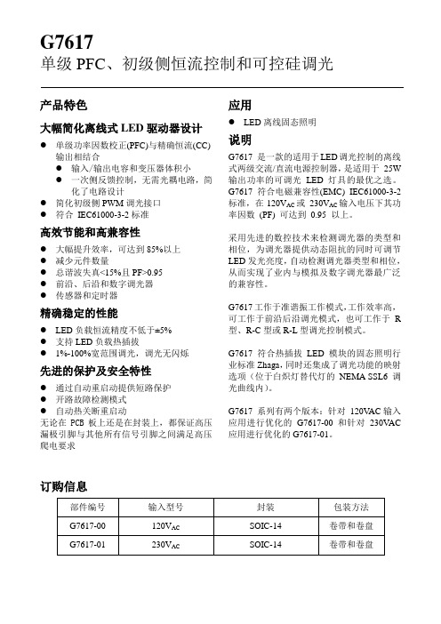
产品特色大幅简化离线式LED驱动器设计●单级功率因数校正(PFC)与精确恒流(CC)输出相结合●输入/输出电容和变压器体积小●一次侧反馈控制,无需光耦电路,简化了电路设计●简化初级侧PWM调光接口●符合IEC61000-3-2标准高效节能和高兼容性●大幅提升效率,可达到85%以上●减少元件数量●总谐波失真<15%且PF>0.95●前沿、后沿和数字调光器●传感器和定时器精确稳定的性能●LED负载恒流精度不低于±5%●支持LED负载热插拔●1%-100%宽范围调光,调光无闪烁先进的保护及安全特性●通过自动重启动提供短路保护●开路故障检测模式●自动热关断重启动无论在PCB板上还是在封装上,都保证高压漏极引脚与其他所有信号引脚之间满足高压爬电要求应用●LED离线固态照明说明G7617 是一款的适用于LED调光控制的离线式两级交流/直流电源控制器,是适用于25W 输出功率的可调光LED 灯具的最优之选。
G7617符合电磁兼容性(EMC) IEC61000-3-2 标准,在120V AC或230V AC输入电压下其功率因数(PF) 可达到0.95 以上。
采用先进的数控技术来检测调光器的类型和相位,为调光器提供动态阻抗的同时可调节LED发光亮度,自动检测调光器类型和相位,从而实现了业内与模拟及数字调光器最广泛的兼容性。
G7617工作于准谐振工作模式,工作效率高,可工作于前沿后沿调光模式,也可工作于R 型、R-C型或R-L型调光控制模式。
G7617 符合热插拔LED 模块的固态照明行业标准Zhaga,同时还集成了调光功能的映射选项(位于白炽灯替代灯的NEMA SSL6 调光曲线内)。
G7617 系列有两个版本:针对120V AC输入应用进行优化的G7617-00 和针对230V AC 应用进行优化的G7617-01。
订购信息应用框图图1典型应用内部框图Vcc VinVcbVT CFGASU BisenseBdrvFdrvFisensePGNDAGND C O R E图2 内部框图引脚功能描述BV SENSE V IN BI SENSE B DRV CFG ASU V CCV CBV TFV SENSEFI SENSEF DRVAGNDPGND 图3. 引脚布局BV SENSE引脚:PFC电感电压反馈点,用于感知Boost电感的磁通状态。
GS3406自动升降压同步600MA芯片
oscillator free running frequency is set slower than the desired synchronized switching frequency to
guarantee sync. The oscillator RT component value required is given by:
80 70 60 50 40 30 20
10
0
1
10
100
1000
output current
VIN=2.7V VIN=3.6V VIN=4.2V
Conversion Efficiency
100
90
80
efficiency
70 60 50 40 30
20
10
0
1
10
100
1000
output current
On Switches B and C
PMOS Switch On Resistance Input Current Limit
Maximum Duty Cycle
Minimum Duty Cycle Frequency Accuracy
升压芯片之34063A_DataSheet
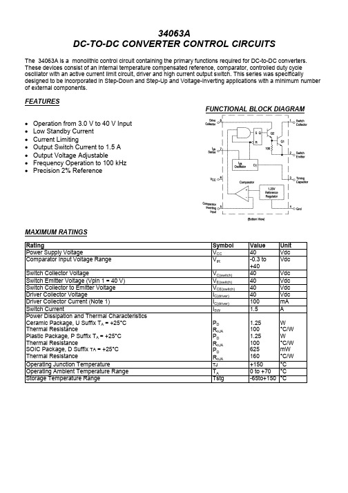
34063ADC-TO-DC CONVERTER CONTROL CIRCUITSThe 34063A is a monolithic control circuit containing the primary functions required for DC-to-DC converters.These devices consist of an internal temperature compensated reference, comparator, controlled duty cycleoscillator with an active current limit circuit, driver and high current output switch. This series was specificallydesigned to be incorporated in Step-Down and Step-Up and Voltage-Inverting applications with a minimum numberof external components.FEATURESFUNCTIONAL BLOCK DIAGRAM• Operation from 3.0 V to 40 V Input • Low Standby Current • Current Limiting • Output Switch Current to 1.5 A • Output Voltage Adjustable • Frequency Operation to 100 kHz • Precision 2% ReferenceMAXIMUM RATINGS Rating Symbol Value Unit Power Supply Voltage V CC 40 VdcComparator Input Voltage Range V IR -0.3 to +40VdcSwitch Collector Voltage V C(switch) 40 VdcSwitch Emitter Voltage (Vpin 1 = 40 V) V E(switch) 40 VdcSwitch Collector to Emitter Voltage V CE(switch) 40 VdcDriver Collector Voltage I C(driver) 40 VdcDriver Collector Current (Note 1) I C(driver) 100 mASwitch Current I SW 1.5 APower Dissipation and Thermal Characteristics Ceramic Package, U Suffix T A = +25°C Thermal Resistance Plastic Package, P Suffix T A = +25°C Thermal Resistance SOIC Package, D Suffix TA = +25°C Thermal Resistance P D R θJAP D R θJA P D R θJA1.25 100 1.25 100 625 160W°C/W W °C/W mW °C/W Operating Junction Temperature TJ +150 °COperating Ambient Temperature Range T A 0 to +70 °CStorage Temperature Range Tstg -65to+150°CORDERING INFORMATIONDevice Temperature RangePackage 34063AD 0° to +70°CSO-8 34063AP1Plastic DIPELECTRICAL CHARACTERICISTICS (V CC = 5.0 V, T A = 0 to +70o C unless otherwise specified.)Characteristics Symbol Min Typ Max UnitOSCILLATORFrequency (V Pin 5 = 0 V, C T = 1.0 nF, T A = 25°C) f osc 24 33 42 kHzCharge Current (V CC = 5.0 V to 40 V, T A = 25°C) I chg 24 33 42 µADischarge Current (V CC = 5.0 V to 40 V, T A = 25°C) I dischg 140 200 260 µADischarge to Charge Current Ratio (Pin7 to Vcc, T A =25°C) I dischg /I chg 5.2 6.2 7.5 —Current Limit Sense Voltage (Ichg = Idischg, T A = 25°C) V lpk (sense) 250300 350 mV OUTPUT SWITCH (Note 3)Saturation Voltage, Darlington Connection (I SW = 1.0 A, Pins 1, 8 connected)V CE (sat) — 1.0 1.3 V Saturation Voltage (I SW = 1.0 A, R Pin 8 = 82 Ω to V CC . Forced β = 20) V CE (sat) — 0.45 0.7 VDC Current Gain (I SW = 1.0 A, V CE = 5.0 V, T A = 25°C) h FE 50 120 — —Collector Off-State Current (V CE = 40V) I C (off) — 0.01 100 µACOMPARATORThreshold Voltage (T A = 25°C) (T A = T LOW to T HIGH ) Vth 1.225 1.21 1.25 — 1.275 1.29V Threshold Voltage (T A = 25°C) ** Vth 1.2375 1.251.2625 VThreshold Voltage Line Regulation (V CC = 3.0 V to 40 V) V REG line 1.4 5.0 mVInput Bias Current (Vin=0V) I IB — -40 -400 nATOTAL DEVICESupply Current (V CC = 5 0 V to 40 V, C T = 1 0 nF, V pin7 = V CC . V Pin5 > Vth, Pin 2 = Gnd, Remaining pins open) I CC2.5 4.0 mANOTES:1. Maximum package power dissipation limits must be observed.2. Low duty cycle pulse techniques are used during test to maintain Junction temperature as close to ambienttemperature as possible3. If the output switch is driven into hard saturation (non Darlington configuration) at low switch currents (< 300 mA) andhigh driver currents (>30 mA), it may take up to 2.0 µs to come out of saturation This condition will shorten the off' timeat frequencies > 30 kHz, and is magnified at high temperatures This condition does not occur with a Darlington configuration,since the output switch cannot saturate If a non Darlington configuration is used, the following output drive condition isrecommendedForced β of output switch = I C , output/(Ic, driver -7.0 mA*) > 10*The 100 Ω. resistor in the emitter of the driver device requires about 7.0 mA before the output switch conducts**Possible version for shipmentPin connection。
IXGH60N60C3;中文规格书,Datasheet资料

GenX3TM 600V IGBTHigh Speed PT IGBT for 40-100kHz SwitchingCES I C110= 60A V CE(sat) ≤ 2.5V t fi (typ)= 50nsSymbol Test Conditions Characteristic Values (T J = 25°C, Unless Otherwise Specified) Min. Typ. Max.BV CES I C = 250μA, V GE = 0V 600V V GE(th)I C= 250μA, V CE = V GE3.05.5VI CES V CE = V CES, V GE = 0V50μAT J = 125°C 1 mA I GES V CE = 0V, V GE = ±20V ±100 nAV CE(sat)I C= 40A, V GE = 15V2.2 2.5 V T J = 125°C1.7 VSymbol Test ConditionsMaximum Ratings V CES T J = 25°C to 150°C600V V CGR T J = 25°C to 150°C, R GE = 1M Ω 600V V GES Continuous ±20V V GEM Transient±30V I C25T C = 25°C (Limited by Leads) 75A I C110T C = 110°C 60A I CM T C = 25°C, 1ms 360A I A T C = 25°C 40A E AST C = 25°C400mJ SSOA V GE = 15V, T VJ = 125°C, R G = 3ΩI CM = 125A (RBSOA) Clamped Inductive Load V CE ≤ V CES P C T C = 25°C380W T J -55 ... +150°C T JM 150°C T stg -55 ... +150°CT LMaximum Lead Temperature for Soldering 300°CT SOLD 1.6 mm (0.062in.) from Case for 10s 260 °C M d Mounting Torque 1.13/10Nm/lb.in.Weight6gFeaturesz Optimized for Low Switching Losses z Square RBSOA z Avalanche ratedzInternational Standard PackageAdvantagesz High Power DensityzLow Gate Drive RequirementApplicationszHigh Frequency Power Inverters z UPSz Motor Drives z SMPSz PFC Circuits z Battery Chargers z Welding Machines zLamp BallastsG = Gate C = Collector E = Emitter Tab = CollectorTO-247 ADTabIXYS Reserves the Right to Change Limits, Test Conditions, and Dimensions.Symbol Test Conditions Characteristic Values (T J = 25°C, Unless Otherwise Specified)fs I C = 40A, V CE ies oes V CE = 25V, V GE res Q g Q ge I C = 40A, V GE Q gc d(on)Notes:1. Pulse test, t ≤ 300μs, duty cycle, d ≤ 2%.2. Switching times & energy losses may increase for higher V CE (Clamp), T J or R G .Inductive Load, TFig. 1. Output Characteristics @ T 304050607080I C - A m p e r e sIXYS Reserves the Right to Change Limits, Test Conditions, and Dimensions.Fig. 7. Transconductance3040506070g f s - S i e m e n sFig. 12. Inductive Switching Energy Lossvs. Gate Resistance1.52.02.53.03.54.0E o f f - M i l l i J o u l e sE off E on - - - -T J = 125ºC , V GE = 15V V CE = 480VIXYS Reserves the Right to Change Limits, Test Conditions, and Dimensions.Fig. 18. Inductive Turn-on Switching Timesvs. Gate Resistance6080100120140 r - N a n o s e c o n d st r t d(on) - - - -T J = 125ºC, V GE = 15V V CE = 480V分销商库存信息: IXYSIXGH60N60C3。
GS3660设计参考资料

GS3660升压电路设计参考
图1TOP层
图2BOTT层
1、图1和图2为PCB layout的版图,GS3660附近走线不要覆铜,要远离MOS管和肖特基整流管和电感这三个器件。
大功率应用中三个元件升温速度快,由于热传导作用,会使GS3660周边RC振荡器件参数发生变化,造成PWM输出波形失真。
2、大电流走线要尽量粗,一般建议使用直接铺成铜皮走线,方便放置过孔的最好可以加过孔。
输入电容的放置建议放在电源输入供电电感附近,输出电容放置在肖特基整流管后面电源输出端,要考虑输入输出电流回路之间尽量短。
3、肖特基二极管和MOS管的选型问题,耐压选择最好高出输出电压的1.1.55倍到两倍的耐压值。
最大通过电流要有足够的余量。
MOS管选择RDS值越小越好,建议选择在10毫欧左右的。
图1中PCB为12V升19V3.5A应用电路,肖特基选择的是STPS2045CT MOS管选择的是AP9974GP。
4、设计时请严格按照我司提供的原理图参数设计,以减少调试中遇到的麻烦。
也可以将设计好的PCB和原理图发到我司相关业务人员的邮箱,我司技术部会协助审核设计文件。
深圳市中广芯源科技有限公司。
思力微GSL3692_DataSheet_Chinese_RevA1.2
4.5. 电路元件...........................................................................................................................................16
3
Silead Inc. 上海思立微电子科技有限公司-多点电容触控 IC
GSL3692 Capacitive Touchscreen Controller
4.3.5. SDA, SCL.....................................................................................................................................15
1.1. 管脚图 .................................................................................................................................................6 1.2. 管脚说明.............................................................................................................................................6 1.3. 原理示意图.........................................................................................................................................9 2. 概述..............................................................................................................................................................9 2.1. 简介 .....................................................................................................................................................9 2.2. 资源 ...................................................................................................................................................11 3. 电容式触控基础.......................................................................................................................................11 3.1. 传感器和节点结构 ..........................................................................................................................11 3.2. 扫描顺序...........................................................................................................................................12 3.3. 触摸屏的灵敏度 ..............................................................................................................................12 4. 操作细节 ...................................................................................................................................................13 4.1. 上电和复位.......................................................................................................................................13 4.2. 校准 ...................................................................................................................................................13 4.3. 通讯 ...................................................................................................................................................13
- 1、下载文档前请自行甄别文档内容的完整性,平台不提供额外的编辑、内容补充、找答案等附加服务。
- 2、"仅部分预览"的文档,不可在线预览部分如存在完整性等问题,可反馈申请退款(可完整预览的文档不适用该条件!)。
- 3、如文档侵犯您的权益,请联系客服反馈,我们会尽快为您处理(人工客服工作时间:9:00-18:30)。
--
Output source current Output sink current
ISOURCE ISINK
VCOMP=450mV
MIN. 495
-1.0 0.78 24
TYP. 500
5 1 -0.2 100 6 0.87 0.05 -40 40
MAX. UNIT
505 mV
20 mV
-
%
1.0 μA
Oscillation frequency Frequency change with voltage Frequency change with temperature
SYMBOL TEST CONDITIONS MIN. TYP. MAX. UNIT
f
RT=3.0KΩ,CT=270pF 400 500 600 KHz
TEL:0755-27668758/29469758
webONAL BLOCK DIAGRAM
3
7
Reference voltage supply
1.25V
0.8V 0.1V
Sawtooth wave oscillator
VCOMP=450mV VCC=2V to 15V Ta = -10℃to 85℃
Input bias current
IB
--
Voltage Gain
Av
--
Frequency bandwidth
BW
Av=0 dB
Output voltage Positive
VPOS
--
Swing
Negative
VNEG
PARAMETER
SYMBOL TEST CONDITIONS
Input source current
ISCP
VSCP= 0V
S.C.P. threshold voltage
VSCP
--
MIN. -1.5 0.7
TYP. -1.0 0.8
MAX. UNIT -0.7 μA 0.9 V
Oscillator section PARAMETER
PARAMETER
SYMBOL TEST CONDITIONS MIN. TYP. MAX. UNIT
Low threshold voltage
VLOW
--
-
-
0.9
V
Upper threshold voltage
VUPPER
--
1.1 1.3 1.5 V
Soft Start section (S.S.) PARAMETER
Input source current Soft start threshold voltage
SYMBOL ISS VSST
TEST CONDITIONS VSCP= 0V --
MIN. -1.5 0.8
TYP. MAX. UNIT -1.0 -0.7 μA 0.9 1.0 V
Short Circuit Protection section (S.C.P.)
0.1V
PWM
1
36kΩ
+ Error Amp.
Comp. + + +
Output drive control circuit
0.5V
500KΩ
DTC 0.6V
0.22V
8
Soft start & SCP circuit
6
2
4
5 30kΩ
MARK VIEW
1 2
GS3660
3 4
PIN DESCRIPTION
GS3660
BOOST CONVERT CONTROL IC
GENERAL DESCRIPTION
The GS3660B is a boost topology switching regulator control IC for battery-used applications field. The GS3660B includes a totem-pole single output stage for driving NPN transistor or N-MOS, high precision reference (0.5V) for comparing output voltage with feedback amplifier, an internal dead-time control for controlling the minimum duty cycle, programmable soft start with short circuit protection function and logic level control for operating mode or standby mode.
Error Amplifier section
PARAMETER
SYMBOL TEST CONDITIONS
Input threshold voltage VT change with voltage VT change with temperature
VFB ΔVFB / ΔV ΔVFB / ΔT
390
-
MAX. UNIT 0.3 V
5000 Ω
0
μA
-45 μA
-0.1 mA
TEL:0755-27668758/29469758
web:
TYPICAL CHARACTERISTICS
Supply Current (mA)
Supply Voltage VS Supply Current
-20 -30
-40 -50
High Level Output Current Iout (mA)
IAVE
RB=390Ω,VCC=0~20V -
TYP. -
5.0
MAX. UNIT
1
μA
10 mA
TEL:0755-27668758/29469758
web:
GS3660
DC ELECTRICAL CHARACTERISTICS (Cont.)
Ambient Temperature Ta (℃)
Figure 3
Input Threshold Voltage Variation △V/V(%)
Low Level Output Voltage Vout (V)
Low Level Output
600
VCC=2V
500
RB=390Ω
Ta=25℃
400
6 OUT 5 O Totem-pole output
GND 6 P IC ground
5
OSC 7
I
Capacitor and resistor connected for the frequency of oscillation
COMP 8 O Error amplifier compensation output
RO
--
MIN. 1.0
0.8
-
-
30 20
TYP. 1.2
1.0
0.1
0.1
-40 40 30
MAX. UNIT
-
V
-
V
0.2 V
0.2 V
-20 mA
-
mA
40 kΩ
Output Current Setting / Control section
PARAMETER
SYMBOL TEST CONDITIONS
Name No. I/O
Description
FB 1 I Error amplifier inverting input pin
8
SCP 2
I
Connected a capacitor Soft start and SCP function pin
7
VCC 3
EN/OFF 4
P IC power supply I Output current setting and control pin
SYMBOL TEST CONDITIONS
VOH1 VOH2 VOL1 VOL2 IOSOURCE IOSINK
RB=390Ω, IO=-15mA RB=750Ω, IO=-10mA, VCC= 1.8V RB=390Ω, IO=15mA RB=750Ω, IO=10mA, VCC= 1.8V RB=390Ω, Vo=0.9V RB=390Ω, Vo=0.3V
FEATURES
˙Wide supply voltage operating range: 1.8 to 15V ˙Reference voltage precision: 2% ˙Low current consumption: Operation Mode 5.5mA
Standby-by Mode 1μA ˙High speed oscillator frequency: 1MHz max. ˙Programmable Soft Start function (SS) ˙Short Circuit Protection function(SCP) ˙Totem-pole output with adjustable on/off current
- V/V
- MHz
V
0.2
-24 μA
-
μA
Output section PARAMETER
Output high voltage
Output high voltage
Output saturation voltage
Output saturation voltage