Jz4755硬件设计指南Jz4755_Board_Design Guide_EN
5G基站建设图纸设计及审核要求
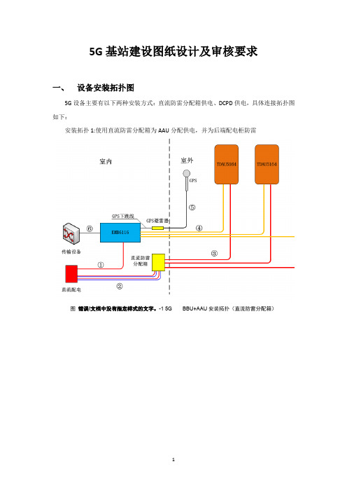
5G基站建设图纸设计及审核要求一、设备安装拓扑图5G设备主要有以下两种安装方式:直流防雷分配箱供电、DCPD供电,具体连接拓扑图如下:安装拓扑1:使用直流防雷分配箱为AAU分配供电,并为后端配电柜防雷图错误!文档中没有指定样式的文字。
-1 5G BBU+AAU安装拓扑(直流防雷分配箱)安装拓扑2:使用DCPD为AAU分配供电,并为后端配电柜防雷。
图错误!文档中没有指定样式的文字。
-2 5GBBU+AAU安装拓扑(DCPD)二、主设备参数2.1 EMB6116参数2.2 TDAU5164N78参数2.3主设备线缆参数三、配套需求设计3.1室内配套设计1、机房平面图需如实反映本次工程机房大小及室内所有设备的尺寸及安装位置,新增设备加粗表示,尺寸标注需齐全、准确。
2、壁挂设备需注明距地高度,并保证所需安装、维护、散热空间,具体要求如下:(1)BBU侧面挂墙面板朝下方式:正前方≥600mm操作空间,顶部≥150mm安全距离,距离地面≥600mm,推荐1200cm-1500mm,距离遮挡物≥500mm操作空间,侧面出风口≥500mm散热空间,进风口≥300mm散热空间。
(2)BBU侧面挂墙面板出风口朝上方式:正前方≥600mm操作空间,顶部≥500mm 散热空间,距离地面≥600mm,推荐1200cm-1500mm,距离遮挡物≥350mm,左侧≥600mm操作空间,右侧≥150mm安全距离。
(3)直流防雷箱挂墙安装,安装空间不小于300mm×245mm×105mm,防雷箱周围足够的走线空间3、设备表需完整反映本机房内所有设备名称、型号、尺寸、数量以及安装属性(原有、新增),此表内容需与预算保持一致。
4、图纸说明需清楚描述本次工程相关信息,主要有以下几点要求:项目归属:描述本次工程归属项目情况站点配置:描述本站设备类型、小区参数配置(EMB6116,TDAU5164N78)机房归属:描述本站机房归属(移动自有、铁塔租用)设备供电:描述本次新增设备需占用的空开大小、数量、位置,核算新增设备功耗并明确是否需新增/更换电源模块、空开,注意:(1)如果使用直流防雷箱进行电源分配,S111配置时,給3个AAU同时供电,双路供电,每路所需最大电流63.75A,直流防雷箱需2路80A空开,BBU需1路63A 空开。
硬件设计技术手册

硬件设计技术手册第一章:引言硬件设计技术手册是一份详细介绍硬件设计技术的文档,旨在为硬件设计工程师提供指导和帮助。
本手册将涵盖硬件设计的各个方面,包括电路设计、PCB设计、硬件测试等内容。
它将涵盖从概念证明到制造的整个硬件生命周期。
第二章:电路设计2.1概述电路设计是硬件设计的核心部分之一。
它包括了模拟电路设计、数字电路设计和混合信号电路设计。
在电路设计过程中,需要了解电路理论、器件特性、损耗、噪音、干扰、时序等相关知识。
2.2模拟电路设计模拟电路设计涵盖了大量的电路设计技术。
包括了放大器设计、滤波器设计、参考源设计等。
此外,还需要熟悉各种电路拓扑结构,并能够根据设备需求进行相应的选择。
2.3数字电路设计数字电路设计应该覆盖数字电路家族的所有基本逻辑门,芯片电路整合、数码电路整合等,需要掌握各类逻辑设计语言和软件,如Verilog、VHDL及各种模拟器等。
2.4混合信号电路设计混合信号电路设计在数字电路和模拟电路的基础上实现模拟和数字混合信号的融合,其中包含硬件的AD、DA转换、软件的仿真等方面的内容。
第三章:PCB设计3.1概述电路板(PCB)是一个重要的硬件配件,PCB的设计影响到硬件的性能、稳定性和可靠性。
在PCB设计中,一定要考虑到PCB板形、布局、层数、连线方式以及PCB排布等各个方面的内容。
3.2PCB设计工具常见的PCB设计工具有Altium Designer、CircuitMaker、Eagle等。
其中Altium Designer是最流行的PCB设计工具之一,其拥有强大的功能和易用的界面,可以帮助用户更快地完成PCB设计。
3.3PCB设计规范在PCB设计中,必须遵守一些规范,以确保PCB具有良好的尺寸、性能和可靠性。
其中包括电路板层数、PCB板形、PCB排布规律、布线方向等。
第四章:硬件测试4.1概述硬件测试是硬件设计的最后一个阶段,目的是确保硬件符合预期的性能和规格。
测试过程中的各种测试手段将涵盖到电路板的功能测试、稳定性测试、可靠性测试以及兼容性测试等内容。
bq20z75 95 PCB 布线指南说明书
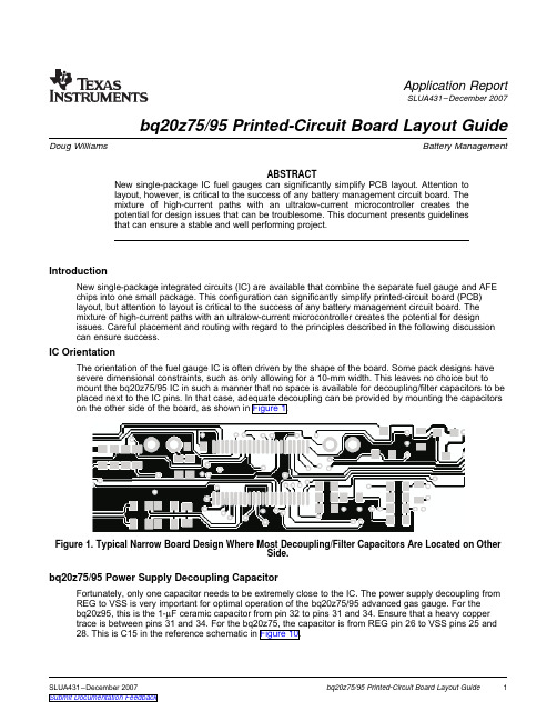
Application ReportSLUA431–December2007 bq20z75/95Printed-Circuit Board Layout Guide Doug Williams Battery ManagementABSTRACTNew single-package IC fuel gauges can significantly simplify PCB layout.Attention tolayout,however,is critical to the success of any battery management circuit board.Themixture of high-current paths with an ultralow-current microcontroller creates thepotential for design issues that can be troublesome.This document presents guidelinesthat can ensure a stable and well performing project.IntroductionNew single-package integrated circuits(IC)are available that combine the separate fuel gauge and AFE chips into one small package.This configuration can significantly simplify printed-circuit board(PCB)layout,but attention to layout is critical to the success of any battery management circuit board.Themixture of high-current paths with an ultralow-current microcontroller creates the potential for designissues.Careful placement and routing with regard to the principles described in the following discussion can ensure success.IC OrientationThe orientation of the fuel gauge IC is often driven by the shape of the board.Some pack designs have severe dimensional constraints,such as only allowing for a10-mm width.This leaves no choice but tomount the bq20z75/95IC in such a manner that no space is available for decoupling/filter capacitors to be placed next to the IC pins.In that case,adequate decoupling can be provided by mounting the capacitors on the other side of the board,as shown in Figure1.Figure1.Typical Narrow Board Design Where Most Decoupling/Filter Capacitors Are Located on OtherSide.bq20z75/95Power Supply Decoupling CapacitorFortunately,only one capacitor needs to be extremely close to the IC.The power supply decoupling from REG to VSS is very important for optimal operation of the bq20z75/95advanced gas gauge.For thebq20z95,this is the1-µF ceramic capacitor from pin32to pins31and34.Ensure that a heavy copper trace is between pins31and34.For the bq20z75,the capacitor is from REG pin26to VSS pins25and28.This is C15in the reference schematic in Figure10.SLUA431–December2007bq20z75/95Printed-Circuit Board Layout Guide1 Ground SystemTo keep the loop area small,place both terminals of this capacitor within3mm of the IC,and centered around pin32(bq20z95)or pin26(bq20z75).Use the shortest possible traces.A large loop area renders the capacitor useless and forms a little loop antenna for noise pickup.Ground SystemThe bq20z75/95requires a low-current ground system separate from the high-current PACK(–)path.Refer to the ground symbols in the bq20z75/95reference designs,and provide the separate low-current ground system accordingly.It is important that the low-current ground system only connects to PACK(–)at the sense resistor Kelvin pick-off point as shown in Figure2.The use of an optional inner layer ground plane is recommended,but not required,for the ground system.Figure2.Diagram Showing bq20z75/95Using Low-Current Ground System for Its Vss Pins andAssociated Components2SLUA431–December2007 bq20z75/95Printed-Circuit Board Layout GuideKevin Connections Kevin ConnectionsKelvin voltage sensing is extremely important in order to accurately measure current and top and bottom cell voltages.Figure3and Figure4demonstrate correct and incorrect techniques,respectively.Figure3.Incorrect Kelvin Voltage Sensing TechniqueIn Figure3,sensing through high-current copper traces produces measurement errors.SLUA431–December2007bq20z75/95Printed-Circuit Board Layout Guide3 RBI and LED CapacitorsFigure4.Correct Kelvin Voltage Sensing TechniqueAs Figure4shows,in some cases,the top and bottom cell voltage sensing may be extended out to the cells.RBI and LED CapacitorsThe3.3-V LEDOUT(pin8)output requires a4.7-µF ceramic capacitor when LEDs are used,but stillrequires2.2µF capacitance for loop stability when LEDs are not used,as with the bq20z75.Thiscapacitor also should be placed as close to the IC as is practical,but several millimeters of copper trace is not a problem.Placement of the RBI capacitor is not as critical.It can be placed further away from the IC.MRST ConnectionRESET and MRST are connected to allow the internal AFE to control the gas gauge reset state.Theconnection between these pins must be as short as possible in order to avoid any incoming noise.The recommended direct interconnection presents no problem.If unwanted resets are found,one or more of the following solutions may be effective:•Add a0.1-µF capacitor between MRST and ground.•Provide a1-kΩpullup resistor to2.5V at RESET.•Surround the entire circuit with a ground pattern.Normally,these steps are not required.If a test pin is added at MRST,provide it with a10-kΩseriesresistor.Communication Line Protection ComponentsThe5.6-V zener diodes,used to protect the communication pins of the bq20z75/95from ESD,should be located as close to the pack connector as possible.Return the grounded end of these zener diodes to the Pack(–)node,rather than to the low-current digital ground system.In this manner,ESD is diverted away from the sensitive electronics as much as possible.4SLUA431–December2007 bq20z75/95Printed-Circuit Board Layout GuideProtector FET Bypass and Pack Terminal Bypass Capacitors Protector FET Bypass and Pack Terminal Bypass CapacitorsThe general principle is to use wide copper traces to lower the inductance of the bypass capacitor circuits.In Figure5,an example layout demonstrates this technique.ing Wide Copper Traces Lowers the Inductance of Bypass Capacitors C1,C2,C3Board Offset ConsiderationsAlthough the most important component for board offset reduction is the decoupling capacitor for REG(2.5V REG),additional benefit is possible by using this recommended pattern for the Coulomb Counterdifferential low-pass filter network.Maintain the symmetrical placement pattern shown for optimum current offset e symmetrical shielded differential traces,if possible,from the sense resistor to the 100-Ωresistors as shown in Figure6.If the current sense leads are long,ensure that the100-Ωresistors are within10–15mm from the IC.Figure6.Differential Filter Components With Symmetrical LayoutSLUA431–December2007bq20z75/95Printed-Circuit Board Layout Guide5 ESD Spark GapESD Spark GapProtect SMBus Clock,Data,and other communication lines from ESD with a spark gap at the connector.The pattern shown in Figure7is recommended,with0,2-mm spacing between the points.Figure7.Recommended Spark Gap Pattern Helps Protect Communication Lines From ESDRadio Frequency InterferenceNormally,strong RF signals have no effect on gas gauge performance.However,any silicon structure can rectify RF signals,producing unwanted voltages and currents at critical nodes.In fact,any copper trace or battery connection has a frequency where it becomes an effective half-wave or quarter-wave receiving antenna.For example,the1900-MHz cell phone band has a quarter wavelength of only3,9cm.A3-watt cell phone,held next to a battery management circuit board,can induce significant errors under the right conditions.Full sweep RF testing for every new design is strongly yout modificationand/or the use of small bypass capacitors can usually mitigate the problem.The most vulnerable node on the bq20z75/95reference design is the SAFE output,which feeds into a signal diode,followed by a FET gate and shunt capacitor.This type of network demodulates an RF signal and can produce enough DC on the gate of the fuse ignition FET to actually ignite the chemical fuse.The solution is to keep the trace from the SAFE output to the diode as short as possible to reduce itseffectiveness as an antenna.Alternately,both sides of the trace can be guarded with grounded copper. Unwanted Magnetic CouplingA battery fuel gauge circuit board is a challenging environment due to the fundamental incompatibility ofhigh-current traces and ultralow-current semiconductor devices.The best way to protect against unwanted trace-to-trace coupling is with a component placement such as that shown in Figure8,where thehigh-current section is on the opposite side of the board from the electronic devices.This is not possible in many situations due to mechanical constraints;nevertheless,every attempt should be made to routehigh-current traces away from signal traces,which enter the bq20z75/95directly.IC voltage references and registers can be disturbed and,in rare cases,damaged due to magnetic and capacitive coupling from the high-current path.Note that during surge current and ESD events,thehigh-current traces appear inductive and can couple unwanted noise into sensitive nodes of the gasgauge electronics,as illustrated in Figure9.6bq20z75/95Printed-Circuit Board Layout Guide SLUA431–December2007Thermal ConsiderationsFigure8.Separating High-and Low-Current Sections Provides an Advantage in Noise ImmunityFigure9.Avoiding Close Spacing Between High-Current and Low-Level Signal LinesThermal ConsiderationsAvoid thermal problems by placing the sense resistor,protection FETS,and high-current traces well away from the ICs.SLUA431–December2007bq20z75/95Printed-Circuit Board Layout Guide7 Reference SchematicReference SchematicFigure10is a reference schematic for a4-series-cell bq20z95battery management fuel gaugeThe bq20z75schematic is similar,but has no LEDs.Figure10.bq20z954-Series-Cell Reference Schematic8bq20z75/95Printed-Circuit Board Layout Guide SLUA431–December2007IMPORTANT NOTICETexas Instruments Incorporated and its subsidiaries(TI)reserve the right to make corrections,modifications,enhancements, improvements,and other changes to its products and services at any time and to discontinue any product or service without notice. Customers should obtain the latest relevant information before placing orders and should verify that such information is current and complete.All products are sold subject to TI’s terms and conditions of sale supplied at the time of order acknowledgment.TI warrants performance of its hardware products to the specifications applicable at the time of sale in accordance with TI’s standard warranty.Testing and other quality control techniques are used to the extent TI deems necessary to support this warranty.Except where mandated by government requirements,testing of all parameters of each product is not necessarily performed.TI assumes no liability for applications assistance or customer product design.Customers are responsible for their products and applications using TI components.To minimize the risks associated with customer products and applications,customers should provide adequate design and operating safeguards.TI does not warrant or represent that any license,either express or implied,is granted under any TI patent right,copyright,mask work right,or other TI intellectual property right relating to any combination,machine,or process in which TI products or services are rmation published by TI regarding third-party products or services does not constitute a license from TI to use such products or services or a warranty or endorsement e of such information may require a license from a third party under the patents or other intellectual property of the third party,or a license from TI under the patents or other intellectual property of TI. Reproduction of TI information in TI data books or data sheets is permissible only if reproduction is without alteration and is accompanied by all associated warranties,conditions,limitations,and notices.Reproduction of this information with alteration is an unfair and deceptive business practice.TI is not responsible or liable for such altered rmation of third parties may be subject to additional restrictions.Resale of TI products or services with statements different from or beyond the parameters stated by TI for that product or service voids all express and any implied warranties for the associated TI product or service and is an unfair and deceptive business practice.TI is not responsible or liable for any such statements.TI products are not authorized for use in safety-critical applications(such as life support)where a failure of the TI product would reasonably be expected to cause severe personal injury or death,unless officers of the parties have executed an agreement specifically governing such use.Buyers represent that they have all necessary expertise in the safety and regulatory ramifications of their applications,and acknowledge and agree that they are solely responsible for all legal,regulatory and safety-related requirements concerning their products and any use of TI products in such safety-critical applications,notwithstanding any applications-related information or support that may be provided by TI.Further,Buyers must fully indemnify TI and its representatives against any damages arising out of the use of TI products in such safety-critical applications.TI products are neither designed nor intended for use in military/aerospace applications or environments unless the TI products are specifically designated by TI as military-grade or"enhanced plastic."Only products designated by TI as military-grade meet military specifications.Buyers acknowledge and agree that any such use of TI products which TI has not designated as military-grade is solely at the Buyer's risk,and that they are solely responsible for compliance with all legal and regulatory requirements in connection with such use.TI products are neither designed nor intended for use in automotive applications or environments unless the specific TI products are designated by TI as compliant with ISO/TS16949requirements.Buyers acknowledge and agree that,if they use anynon-designated products in automotive applications,TI will not be responsible for any failure to meet such requirements. Following are URLs where you can obtain information on other Texas Instruments products and application solutions:Products ApplicationsAmplifiers AudioData Converters AutomotiveDSP BroadbandInterface Digital ControlLogic MilitaryPower Mgmt Optical NetworkingMicrocontrollers SecurityRFID TelephonyLow Power Video&ImagingWirelessWirelessMailing Address:Texas Instruments,Post Office Box655303,Dallas,Texas75265Copyright©2007,Texas Instruments Incorporated。
国家仪器(National Instruments)产品快速参考指南说明书
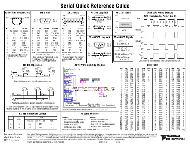
ASCII Table
Dec Hex Char 32 0x20 (sp) 33 0x21 ! 34 0x22 “ 35 0x23 # 36 0x24 $ 37 0x25 % 38 0x26 & 39 0x27 ‘ 40 0x28 ( 41 0x29 ) 42 0x2A * 43 0x2B + 44 0x2C , 45 0x2D 46 0x2E . 47 0x2F / 48 0x30 0 49 0x31 1 50 0x32 2 51 0x33 3 52 0x34 4 53 0x35 5 54 0x36 6 55 0x37 7 56 0x38 8 57 0x39 9 58 0x3A : 59 0x3B ; 60 0x3C < 61 0x3D = 62 0x3E > 63 0x3F ?
1 0011 0110
Idle
RS-232 +5 V
S 0 1 2 3 4 5 6 7 P S Idle
RS-485/422 Signals
If '–' < '+' then MARK, '1'
If '–' > '+' then SPACE, '0' RS-422 Voltage: ±7 V RS-485 Voltage:
Pin 14
Pin 25
Pin
232
2
TXD
3
RXD
4
RTS
5
CTS
6
DSR3
7
GND
8
DCD3
20
DTR3
22
RI3
422/485 RTS+ (HSO+) CTS+ (HSI+) RTS– (HSO–)
心率检测在智能手表上的应用_李志强
信号,然后接收组织的反射光信号。测量组织容积在 心脏搏动时的微小变化造成的反射光强度变化,来获
得脉搏波信号,通过检测峰值获得心率。 理论上还有一种做法是使用双波长光信号,通过
光电容积法测量获得血氧饱和度值,光信号需要进行
调制,双波长光线轮流照射组织,获得了每一时刻组 织对两种不同波长光线的反射光强度。然后进行解调 并根据朗伯比尔定律计算出血氧饱和度值。但是由于 该检测方法在手表上运用准确度不够,目前比较少产 品有做血氧检测。
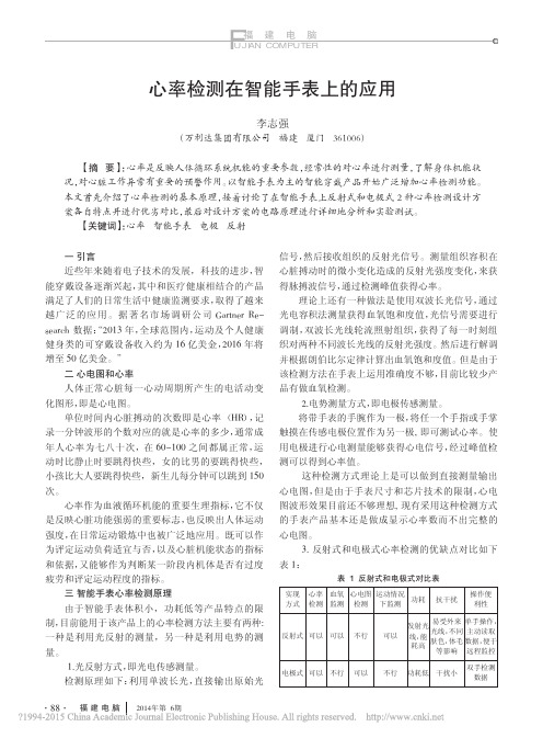
心电图。 3. 反射式和电极式心率检测的优缺点对比如下
表 1:
表 1 反射式和电极式对比表
实现 心率 血氧 心电图 运动情况
操作便
功耗 抗干扰
方式 检测 监测 检测 下监测
利性
反射式 可以 可以 不行
可以
易受外来 单手操作, 发射光
光线,不同 主动读取 线,能
肤色,体毛 数据,便于 耗高
等影响 远程监控
参考文献:
[1]1. 神念科技官网 / [2]2. 北京君正官网 /cn/cn/proinfo.php? id=14&pid=782&fid=782
[3]3. 德 州 仪 器 官 网014 年第 6 期
F福 建 电 脑 UJIAN COMPUTER
心率检测在智能手表上的应用
李志强
(万利达集团有限公司 福建 厦门 361006)
【摘 要】:心率是反映人体循环系统机能的重要参数,经常性的对心率进行测量,了解身体机能状 况,对心脏工作异常有重要的预警作用。以智能手表为主的智能穿戴产品开始广泛增加心率检测功能。 本文首先介绍了心率检测的基本原理,接着讨论了在智能手表上反射式和电极式 2 种心率检测设计方 案各自特点并进行优劣对比,最后对设计方案的电路原理进行详细地分析和实验测试。
475 说明书
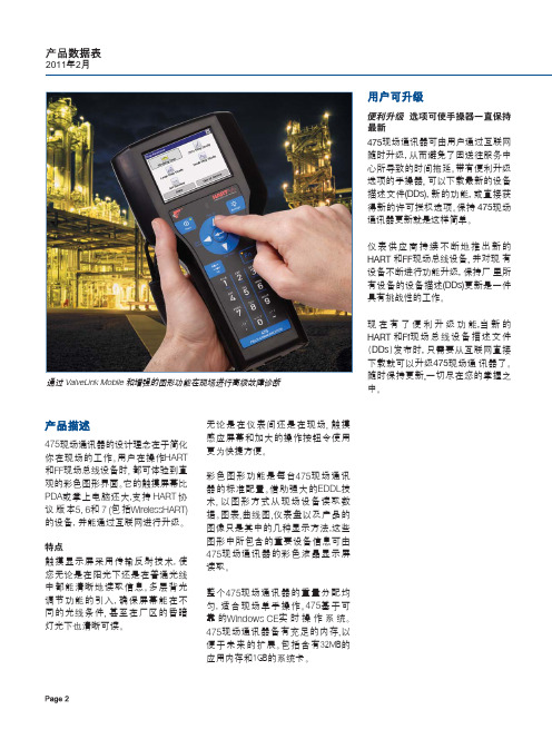
现 在 有 了 便 利 升 级 功 能,当 新 的 HART 和Ff现 场 总 线 设 备 描 述 文 件 (DDs)发布时, 只需要从互联网直接 下载就可以升级475现场通 讯器了。 随时保持更新,一切尽在您的掌握之 中。
使用 -10°C (14°F ) 到+50°C (122°F ) 0% to 95% RH (无凝结) 从0°C (32°F) 到+50°C (122°F )
充电 10°C (32°F ) 到+40°C (104°F )
带电池储存 -20°C (-4°F ) 到+55°C (131°F )
无电池储存 -20°C (-4°F ) 到+55°C (131°F )
外壳保护级别 IP51(前部)
防撞击 测试通过1米自由落体到水泥表面
便利升级要求
使用 有Internet连接的PC CD Rom驱动器 IrDA口(或红外适配器) 蓝牙接口(或适配器) SD 读卡器(对某些升级需要) WindowsXP(SP2 或SP3)或 Windows Vista 商务版(SP1) 操作系统
键盘 共25键,包括4个动作键,12个数字字母键, tab键,功能键,背光键,电源键,和4个光标 控制(箭头)键
电池 可充电锂离子电池模块
电池运行时间 连续运行-20小时 常规使用-40小时 待机状态-80小时
电池充电器选项 输入电压100-240VAC,50-60Hz 包括电源线,插头有美国,欧洲,和英国选择
对 于HART回 路, 475现 场 通 讯 器 能 确认回路中的DC信号是否正确。
通信电子线路课程设计--调频发射系统整机电路设计

通信电子线路课程设计--调频发射系统整机电路设计随着人类的文明不断进步,科学技术不断的发展,人们之间的交流越来越多,相互交换的信息也日益剧增,要传送的信息类型也是越来越多样化。
科技的进步也使得通信的技术得到了发展,特别是无线电波的使用,使我们的通信更加实时、高效。
科技的快速发展,将使人们的通信更方便快捷。
随着科技的发展和人民生活水平的提高,无线电发射机在生活中得到广泛应用,最普遍的有电台、对讲机等。
人们通过无线电发射机可以把需要传播出的信息发射出去,接收者可以通过特制的接收机接受信息,最普通的模式是:广播电台通过无线电发射机发射出广播,收听者通过收音机即可接收到电台广播。
调频发射机目前处于快速发展之中,在很多领域都有了很广泛的应用。
它可以用于演讲、教学、玩具、防盗监控等诸多领域。
关键字:高频电子线路,Multisim仿真,调频发射。
一、前言 (1)二、设计指标 (2)2.1题目 (2)2.2设计任务及主要技术指标和要求 (2)2.3内容和要求 (2)2.4主要技术指标 (2)三、系统总述 (3)3.1 调频基本概念 (3)3.2 工作原理 (3)3.3整体原理框图 (5)四、单元电路设计与仿真 (6)4.1压控振荡器调频电路 (6)4.2变容二极管直接调频电路 (8)4.3上混频电路 (10)4.4三极管倍频电路 (11)4.5丙类谐振功率放大电路 (12)五、整机电路设计 (13)六、高频实验平台整机联调 (14)七、设计总结 (16)八、参考文献 (17)一、前言频率的调制和解调是通信电子线路中非常重要且比较关键的一部分,调频电路在通信电子线路中运用非常广泛且作用很大,如何学好此部分对我们来说非常重要。
本课程设计的内容是学习基于Multisim的调频电路设计与仿真。
用Multisim仿真软件进行调频电路调频和解调,得到仿真结果。
从仿真结果中更好地理解频率的调制和解调。
由于一般的低频信号无法进行远距离传输,所以得经过调频搬到高频信号上传输,这个过程就是我们常说的调频。
产品硬件详细设计规范

收文:XXX * 非经本公司同意,严禁影印*XXXXXXXX有限公司收文:05-02C* 非经本公司同意,严禁影印*收文:05-03C * 非经本公司同意,严禁影印*文:*非经公司同意, 严禁影印*文:*非经公司同意, 严禁影印**非经公司同意, 严禁影印*文:*非经公司同意, 严禁影印*文:*非经公司同意, 严禁影印*文:*非经公司同意, 严禁影印*文:*非经公司同意, 严禁影印*文:*非经公司同意, 严禁影印*□硬件模块调试报告□产品硬件测试报告收文:05-05C * 非经公司同意, 严禁影印**非经公司同意, 严禁影印**非经公司同意, 严禁影印**非经公司同意, 严禁影印**非经公司同意, 严禁影印**非经公司同意, 严禁影印*收文:05-05C *非经公司同意, 严禁影印*收文:05-05C *非经公司同意, 严禁影印*收文:05-05C *非经公司同意, 严禁影印*收文:05-05C *非经公司同意, 严禁影印*收文:05-05C * 非经公司同意, 严禁影印*05-05C *非经公司同意, 严禁影印*收文:05-05C *非经公司同意, 严禁影印*收文:05-05C *非经公司同意, 严禁影印*收文:05-05C *非经公司同意, 严禁影印*收文:05-05C *非经公司同意, 严禁影印*收文:05-05C *非经公司同意, 严禁影印*收文:05-05C *非经公司同意, 严禁影印*收文:05-05C *非经公司同意, 严禁影印*收文:05-05C *非经公司同意, 严禁影印*收文:05-05C *非经公司同意, 严禁影印*收文:05-05C *非经公司同意, 严禁影印*收文:05-05C *非经公司同意,严禁影印*收文:05-05C *非经公司同意, 严禁影印*收文:05-05C *非经公司同意, 严禁影印*收文:05-05C *非经公司同意, 严禁影印*收文:05-05C*非经公司同意, 严禁影印*XXXXXXXX有限公司收文:05-05C *非经公司同意, 严禁影印*收文:05-05C *非经公司同意, 严禁影印*]收文:05-05C *非经公司同意, 严禁影印*收文:05-05C *非经公司同意, 严禁影印*收文:05-05C *非经公司同意, 严禁影印*收文:05-05C *非经公司同意, 严禁影印*收文:05-05C *非经公司同意, 严禁影印*收文:05-05C *非经公司同意, 严禁影印*收文:05-05C *非经公司同意, 严禁影印*XXXXXXXX有限公司收文: 05-05C。
- 1、下载文档前请自行甄别文档内容的完整性,平台不提供额外的编辑、内容补充、找答案等附加服务。
- 2、"仅部分预览"的文档,不可在线预览部分如存在完整性等问题,可反馈申请退款(可完整预览的文档不适用该条件!)。
- 3、如文档侵犯您的权益,请联系客服反馈,我们会尽快为您处理(人工客服工作时间:9:00-18:30)。
All information in this document should be treated as preliminary. Ingenic may make changes to this document without notice. Anyone relying on this documentation should contact Ingenic for the current documentation and errata.
Ingenic® Jz4755
Board Design Guide
Revision: 1.0 Date: Sep. 2009
Ingenic Jz4755
Board Design Guide
Copyright © Ingenic Semiconductor Co. Ltd 2009. All rights reserved.
3 External Memory Interface Design Guidelines .................................. 7
3.1 Overview ................................................................................................................................. 7 3.2 Memory sub-system................................................................................................................ 7
2 Platform Stack-Up and Placement ..................................................... 3
2.1 General Design Considerations.............................................................................................. 3 2.2 Nominal 4-Layer Board Stack-Up ........................................................................................... 3 2.3 PCB Technology Considerations ............................................................................................ 4
5 Video Design Guidelines ................................................................. 15
5.1 Video Power.......................................................................................................................... 15 5.2 VIDEO Out ............................................................................................................................ 15
3.2.1 Boot Memory ................................................................................................................... 7 3.2.2 NAND Flash Connection ................................................................................................. 8 3.3 SDRAM ................................................................................................................................... 8
9.1 Touch Screen ........................................................................................................................ 23 9.2 Battery Voltage Measurement..................................................................................y
Date Sep. 2009
Revision
1.0
First release
Change
Disclaimer
This documentation is provided for use with Ingenic products. No license to Ingenic property rights is granted. Ingenic assumes no liability, provides no warranty either expressed or implied relating to the usage, or intellectual property right infringement except as provided for by Ingenic Terms and Conditions of Sale.
8 Camera ............................................................................................ 21
9 SAR A/D Controller .......................................................................... 23
Ingenic Semiconductor Co., Ltd.
Room 108, Information Center Block A Zhongguancun Software Park, 8 Dongbeiwang west Road, Haidian District, Beijing China, 100193 Tel: 86-10-82826661 Fax: 86-10-82825845 Http: //
6 USB Design Guidelines ................................................................... 17
7 LCD ................................................................................................. 19
Content
Content
1 Overview............................................................................................ 1
1.1 Introduction ............................................................................................................................. 1 1.2 Reference Platform ................................................................................................................. 2
4 Audio Design Guidelines ..................................................................11
4.1 Audio Power...........................................................................................................................11 4.2 Headphone Out......................................................................................................................11 4.3 Mic In..................................................................................................................................... 12 4.4 Line In ................................................................................................................................... 12 4.5 Layout Guideline ................................................................................................................... 12