LDQ-M282RI, 规格书,Datasheet 资料
2SC2881-Y(TE12L,CF;中文规格书,Datasheet资料

TOSHIBA Transistor Silicon NPN Epitaxial Type (PCT process)2SC2881Voltage Amplifier Applications Power Amplifier Applications• High voltage: V CEO = 120 V• High transition frequency: f T = 120 MHz (typ.) • Small flat package• P C = 1.0 to 2.0 W (mounted on ceramic substrate) • Complementary to 2SA1201Absolute Maximum Ratings (Ta = 25°C)Characteristics Symbol Rating UnitCollector-base voltage V CBO 120 V Collector-emitter voltage V CEO 120 V Emitter-base voltage V EBO 5 V Collector current I C 800 mA Base currentI B 160 mA P C500 Collector power dissipationP C (Note 1)1000mWJunction temperature T j 150 °C Storage temperature rangeT stg−55 to 150°CNote 1: Mounted on a ceramic substrate (250 mm 2 × 0.8 t)Note 2: Using continuously under heavy loads (e.g. the application of high temperature/current/voltage and the significant change in temperature, etc.) may cause this product to decrease in the reliability significantly even if the operating conditions (i.e. operating temperature/current/voltage, etc.) are within the absolute maximum ratings.Please design the appropriate reliability upon reviewing the Toshiba Semiconductor Reliability Handbook (“Handling Precautions”/Derating Concept and Methods) and individual reliability data (i.e. reliability test report and estimated failure rate, etc).Unit: mmPW-MINI JEDEC―JEITA SC-62 TOSHIBA 2-5K1AWeight: 0.05 g (typ.)Electrical Characteristics (Ta = 25°C)Characteristics Symbol TestCondition MinTyp.Max UnitCollector cut-off current I CBO V CB = 120 V, I E = 0 ―― 0.1 μAEmitter cut-off current I EBO V EB = 5 V, I C = 0 ――0.1 μA Collector-emitter breakdown voltage V (BR) CEO I C = 10 mA, I B = 0 120 ―― V Emitter-base breakdown voltage V (BR) EBO I E = 1 mA, I C = 0 5 ―― VDC current gain h FE(Note 3)V CE = 5 V, I C = 100 mA 80 ―240―Collector-emitter saturation voltage V CE (sat)I C = 500 mA, I B = 50 mA ―― 1.0 V Base-emitter voltage V BE V CE = 5 V, I C = 500 mA ―― 1.0 V Transition frequency f T V CE = 5 V, I C = 100 mA ― 120 ― MHz Collector output capacitance C ob V CB = 10 V, I E = 0, f = 1 MHz ―― 30 pF Note 3: h FE classification O: 80 to 160, Y: 120 to 240MarkingNote 4: A line under a Lot No. identifies the indication of product Labels.Not underlined: [[Pb]]/INCLUDES > MCVUnderlined: [[G]]/RoHS COMPATIBLE or [[G]]/RoHS [[Pb]]Please contact your TOSHIBA sales representative for details as to environmental matters such as the RoHScompatibility of Product. The RoHS is the Directive 2002/95/EC of the European Parliament and of the Council of 27 January 2003 on the restriction of the use of certain hazardous substances in electrical and electronic equipment.Ambient temperature Ta (°C)P C – TaC o l l e c t o r p o w e r d i s s i p a t i o n P C (W )Collector-emitter voltage V CE (V)I C – V CEC ol l e ct o r c u r r e n t I C(m A )Collector current I C (mA)h FE – ICD C c u r r e n t g a i nh F ECollector current I C (mA)V CE (sat) – I CC o l l e c t o r -e m i t t e r s a t u r a t io n vo l t a g e V C E (s at ) (V )Base-emitter voltage V BE (V)I C – V BECol l e c t o r c u rr e n tI C (A )Collector-emitter voltage V CE (V)Safe Operating AreaC o ll e c t o r c u r r e n t I C (m A )0.3 3 1 10 10030 300RESTRICTIONS ON PRODUCT USE•Toshiba Corporation, and its subsidiaries and affiliates (collectively “TOSHIBA”), reserve the right to make changes to the information in this document, and related hardware, software and systems (collectively “Product”) without notice.•This document and any information herein may not be reproduced without prior written permission from TOSHIBA. Even with TOSHIBA’s written permission, reproduction is permissible only if reproduction is without alteration/omission.•Though TOSHIBA works continually to improve Product’s quality and reliability, Product can malfunction or fail. Customers are responsible for complying with safety standards and for providing adequate designs and safeguards for their hardware, software and systems which minimize risk and avoid situations in which a malfunction or failure of Product could cause loss of human life, bodily injury or damage to property, including data loss or corruption. Before customers use the Product, create designs including the Product, or incorporate the Product into their own applications, customers must also refer to and comply with (a) the latest versions of all relevant TOSHIBA information, including without limitation, this document, the specifications, the data sheets and application notes for Product and the precautions and conditions set forth in the “TOSHIBA Semiconductor Reliability Handbook” and (b) theinstructions for the application with which the Product will be used with or for. Customers are solely responsible for all aspects of their own product design or applications, including but not limited to (a) determining the appropriateness of the use of this Product in such design or applications; (b) evaluating and determining the applicability of any information contained in this document, or in charts, diagrams, programs, algorithms, sample application circuits, or any other referenced documents; and (c) validating all operating parameters for such designs and applications. TOSHIBA ASSUMES NO LIABILITY FOR CUSTOMERS’ PRODUCT DESIGN OR APPLICATIONS.•Product is intended for use in general electronics applications (e.g., computers, personal equipment, office equipment, measuring equipment, industrial robots and home electronics appliances) or for specific applications as expressly stated in this document.Product is neither intended nor warranted for use in equipment or systems that require extraordinarily high levels of quality and/or reliability and/or a malfunction or failure of which may cause loss of human life, bodily injury, serious property damage or serious public impact (“Unintended Use”). Unintended Use includes, without limitation, equipment used in nuclear facilities, equipment used in the aerospace industry, medical equipment, equipment used for automobiles, trains, ships and other transportation, traffic signaling equipment, equipment used to control combustions or explosions, safety devices, elevators and escalators, devices related to electric power, and equipment used in finance-related fields. Do not use Product for Unintended Use unless specifically permitted in this document.•Do not disassemble, analyze, reverse-engineer, alter, modify, translate or copy Product, whether in whole or in part.•Product shall not be used for or incorporated into any products or systems whose manufacture, use, or sale is prohibited under any applicable laws or regulations.•The information contained herein is presented only as guidance for Product use. No responsibility is assumed by TOSHIBA for any infringement of patents or any other intellectual property rights of third parties that may result from the use of Product. No license to any intellectual property right is granted by this document, whether express or implied, by estoppel or otherwise.•ABSENT A WRITTEN SIGNED AGREEMENT, EXCEPT AS PROVIDED IN THE RELEVANT TERMS AND CONDITIONS OF SALE FOR PRODUCT, AND TO THE MAXIMUM EXTENT ALLOWABLE BY LAW, TOSHIBA (1) ASSUMES NO LIABILITYWHATSOEVER, INCLUDING WITHOUT LIMITATION, INDIRECT, CONSEQUENTIAL, SPECIAL, OR INCIDENTAL DAMAGES OR LOSS, INCLUDING WITHOUT LIMITATION, LOSS OF PROFITS, LOSS OF OPPORTUNITIES, BUSINESS INTERRUPTION AND LOSS OF DATA, AND (2) DISCLAIMS ANY AND ALL EXPRESS OR IMPLIED WARRANTIES AND CONDITIONS RELATED TO SALE, USE OF PRODUCT, OR INFORMATION, INCLUDING WARRANTIES OR CONDITIONS OF MERCHANTABILITY, FITNESS FOR A PARTICULAR PURPOSE, ACCURACY OF INFORMATION, OR NONINFRINGEMENT.•Do not use or otherwise make available Product or related software or technology for any military purposes, including without limitation, for the design, development, use, stockpiling or manufacturing of nuclear, chemical, or biological weapons or missile technology products (mass destruction weapons). Product and related software and technology may be controlled under the Japanese Foreign Exchange and Foreign Trade Law and the U.S. Export Administration Regulations. Export and re-export of Product or related software or technology are strictly prohibited except in compliance with all applicable export laws and regulations. •Please contact your TOSHIBA sales representative for details as to environmental matters such as the RoHS compatibility of Product.Please use Product in compliance with all applicable laws and regulations that regulate the inclusion or use of controlled substances, including without limitation, the EU RoHS Directive. TOSHIBA assumes no liability for damages or losses occurring as a result of noncompliance with applicable laws and regulations.分销商库存信息: TOSHIBA2SC2881-Y(TE12L,CF。
实验四、三层交换机的使用
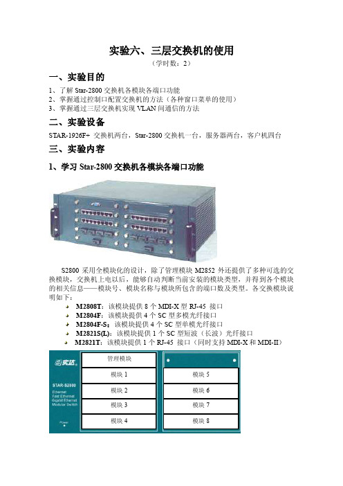
实验六、三层交换机的使用(学时数:2)一、实验目的1、了解Star-2800交换机各模块各端口功能2、掌握通过控制口配置交换机的方法(各种窗口菜单的使用)3、掌握通过三层交换机实现VLAN 间通信的方法二、实验设备STAR-1926F+ 交换机两台,Star-2800交换机一台,服务器两台,客户机四台三、实验内容1、学习Star-2800交换机各模块各端口功能S2800采用全模块化的设计,除了管理模块M2852外还提供了多种可选的交换模块,交换机上电以后,能够自动判断当前安装的模块类型,并得到各个模块的相关信息——模块号、模块名称与模块所包含的端口数及类型。
各交换模块说明如下:M2808T :该模块提供8个MDI-X 型RJ-45 接口M2804F :该模块提供4个SC 型多模光纤接口M2804F-S :该模块提供4个SC 型单模光纤接口M2821S(L):该模块提供1个SC 型短波(长波)光纤接口M2821T :该模块提供1个RJ-45 接口(同时支持MDI-X 和MDI-II )管理模块 模块1 模块4模块3 模块2 模块8模块7 模块6 模块5M2808T1)10Mbps-半双工2)10Mbps-全双工3)100Mbps-半双工4)100Mbps-全双工M2804F Array M2804F模块提供了4个SC型快速以太网光纤接口,这些端口支持100Mbps-半双工与100Mbps-全双工2种工作模式。
M2821S(L) Array M2821S/L模块提供了1个SC型的千兆以太网光纤接口,端口支持1000Mbps-半双工与1000Mbps-全双工2种工作模式。
M2821T Array M2821T模块提供了1个10/100/1000M自适应RJ45口,端口支持6种工作模式:1)10Mbps-半双工2)10Mbps-全双工3)100Mbps-半双工4)100Mbps-全双工5)1000Mbps-半双工6)1000Mbps-全双工2、通过Console口配置交换机●将交换机通过Console口与一计算机的COM1口相联●启动登录:开始→程序→附件→通讯→超级终端三层交换机STAR2800配置窗口Port VLAN工作方式方式窗口Tag VLAN工作方式方式窗口3、通过三层交换机实现VLAN 间通信(1) 对于实验环境一Switch A Switch BS-2800实验过程1、连接:用交叉线将S-2800的8/7端口与Switch A的端口24相连;用交叉线将S-2800的8/8端口与Switch B的端口24相连。
INH281M-2[1]
![INH281M-2[1]](https://img.taocdn.com/s3/m/f29855166edb6f1aff001fab.png)
INH281M(I)-2 Series Product InformationDescription(描述)直流瞬态浪涌电压是指在直流供电网络中,受系统中各种负载干扰产生的超出正常供电的过压/欠压浪涌脉冲。
若不加保护,过高的瞬态浪涌电压会导致用电设备电子器件的损伤或失效。
直流浪涌保护模块,应用于用电设备电源输入端,采用有源器件对过高瞬态浪涌电压进行跟踪并抑制,保证输出电压始终维持在设备允许的供电范围之内,超出正常供电部分的电压能量被浪涌保护模块转化为热能吸收掉,从而达到净化供电的目的,保证系统可靠地工作。
来自瑞典MAGIC公司的DC浪涌保护模块系列产品具有体积小、功耗低、带载能力强、可靠性高、自失效保护及防反接自动保护等优点,对航空、航天等领域供电输入端瞬态浪涌抑制具有显著的效果。
已被全球众多航空电子设备供应商广泛采用。
Feature(功能)宽电源输入范围,无需额外提供电源INH281M-2:8~32VINH281M-2-H:8~36V16×26×9mm超小体积,低功耗,高可靠性,PCB安装方式2A额定工作电流下能承受80V/100ms或100V/50ms浪涌冲击80V过压浪涌发生时输出电压箝位INH281M-2:< 35VINH281M-2-H:< 38V8V欠压浪涌发生时输出电压跟随输入电压出色的尖峰浪涌吸收能力出色的自我保护功能。
自身损坏时能自动切断电源输出,保护自身和系统不受损伤电源输入反接自保护。
电源输入端极性反接时能自动切断输出,避免系统受反压冲击损坏 良好的单向通过性,连续导通工作时仅损耗50mV/A的压降符合MIL-STD-704A/D/E/F,DO160E cat A/B/ Z,EN2282,AIR2021EABSOLUTE MAXIMUM RATINGS (极限环境)瞬态浪涌输入电压/持续时间(I OUT =2A ): 100V/70ms ,80V/100ms 极限持续输入电压V IN : INH281M-2:8~32VINH281M-2-H :8~36V极限持续输出电流I OUT : 3A 极限工作温度: 工业级:-40℃~+70℃军用级:-55℃~+85℃ 宇航级:-55℃~+105℃贮存温度: -65℃~+125℃ 焊接温度(3秒): 280℃Electrical Characteristics, TA=25℃(电参数特性)存储温度-65℃~+125℃ 测试条件(T A =+25℃)参数最小 典型 最大 单位输入/输出隔离耐压 150 V 输入/外壳隔离耐压 1500 V 输出纹波(20MH 带宽) 50 mV P-P INH281M-2 8 28 32额定工作电压V ININH281M-2-H8 28 36V输入-输出压差 (非浪涌阶段) △V 40 42 50 mV/A 额定输出电压V OUTV IN -△VV稳态输出电流I OUT 2 2.5 A 瞬态浪涌输入电压V INS 8 80 V 欠压浪涌输出电压V OUTV IN -V△ VINH281M-2 33 35过压浪涌输出电压V OUTINH281M-2-H36 38 V瞬态浪涌持续时间(V INS =80V)50100 ms瞬态峰值功率110 W 耗散功率(V IN =28V ,I OUT =2A) 560 600 660 mW 相邻浪涌间隔时间10 60 sTypical Application (典型应用电路)注: 1. 为避免欠压浪涌期间储能电容通过反向回路将能量释放到电网上,建议在电网输入端接入相应的大功率肖特基二极管。
D2MQ系列微型基本切换器说明书

D 2M QUltra Slim Snap-actionSwitch with 2.7 mm in depth●Excellent electrical characteristics and snap action mechanism in spite of its ultra small size. ●Ideal for applications where size is extremely limited and high reliability is demanded.RoHS CompliantModel Number Legendthe Switch is viewed from the direction of the arrow in the drawing below.Contact Form●SPDTContact SpecificationsD2MQ-1@@@ 3. Terminal s None : PCB termin a l s (S tr a ight) -TL : PCB Termin a l s (Left-a ngled) -TR : PCB Termin a l s (Right-a ngled)1. ActuatorNone : Pin pl u nger L : Le a f lever 2. S witchin g capacity None : 30 VDC 0.5A -105 : 30 VDC 50mA<Hinge lever>D2MQ-@@-1@ 3. Terminal s None : PCB termin a l s (S tr a ight) -L : PCB Termin a l s (Left-a ngled) -R : PCB Termin a l s (Right-a ngled)1. Actuator4L: Hinge lever 2. Ratin gsNone : 30 VDC 0.5A -105 : 30 VDC 50mA123123ItemModel0.5 A models50 mA modelsContactSpecification RivetMaterial Silver platedGold platedGap(standard value)0.15 mmMinimum applicable load (see note)5 VDC 50 mA5 VDC 5 mAD2MQ Subminiature Basic SwitchD 2 M Q RatingsNote.The above rating values apply under the following test conditions.(1) Ambient temperature: 20±2°C(2) Ambient humidity: 65±5%(3) Operating frequency: 30 operations/minCharacteristicsNote.The data given above are initial values.*1.For the pin plunger models, the above values apply for use at the freeposition and total travel position. For the lever models, they apply at thetotal travel position. Close or open circuit of the contact is 1ms max.*2.For testing conditions, consult your OMRON sales representative. Terminals/Appearances (Unit:mm)●PCB terminals (Straight) ●PCB terminals (Left-angled)●PCB terminals (Right-angled) <PCB Mounting Dimensions (Reference)>Mounting Holes (Unit: mm)Type0.5A models 50mA modelsRated voltage Item Resistive load30 VDC0.5A 50 mAPermissible operating speed0.1 mm to 0.5 mm/s (for pin plungermodels)PermissibleoperatingfrequencyMechanical 60operations/minElectrical 30 operations/minInsulation resistance100 MΩ min. (at 250 VDC with insulationtester)Contact resistance (initial value) 100 mΩ max.DielectricstrengthBetweenterminals of thesame polarity500 VAC 50/60 Hz 1minBetweencurrent-carryingmetal parts andground500 VAC 50/60 Hz 1minVibrationresistance * 1Malfunction 10 to 55 Hz, 1.5 mm double amplitudeShockresistanceDurability 1,000m/s2 {approx. 100G} max.Malfunction * 1300 m/s2 {approx. 30G} max.Durability * 2Mechanical 30,000 operations min. (60 operations/min)Electrical 10,000operationsmin.(30 operations/min)Degree of protection IEC IP40Ambient operating temperature−15°C to +70°C (at ambient humidity of60% max.)(with no icing or condensation)Ambient operating humidity 35% to 85% (for +5°C to +35°C)Weight Approx.0.3g 2-1.6+0.12-1.6+0.12-1.6+0.10a. hole s* Termin a l g a p i s 1 pitch2-1.6 di a. mo u nting hole sD2MQSubminiature Basic SwitchD2M QDimensions (Unit: mm) /Operating CharacteristicsThe illustrations and drawings are for PCB terminals (straight) models.Refer to "Terminals/Appearances" of the previous page for details on models with PCB terminals (Right-angled) and PCB terminals (Left-angled).Note 1.Unless otherwise specified, a tolerance of ±0.15 mm applies to all dimensions. Note 2.The operating characteristics are for operation in the A direction ().Precautions★Please refer to "Basic Switches Common Precautions" for correct use.●Soldering•Terminal connectionsWhen soldering terminals manually, perform soldering within 3 seconds at iron tip temperature no higher than 300°C. Do not apply any external force for 1 minute after soldering. When applying solder, keep the solder away from the case of the Switch and do not allow solder or flux to flow into the case. It is recommended that you apply flux guard to the mounting surface of the Switch.●MountingUse M1.4 mounting screw with plane washers or spring washers to securely mount the Switch. Tighten the screws to a torque of 0.08 to 0.1 N·m {0.8 to 1 kgf·cm}.●Operation•Do not apply a force more than two times the rated operating force to the actuator and leaf lever.•Provide an amount of OT that equals or exceeds the standard. •Do not change the operating position by modifying the actuator.•Do not use the Switch in an application where the operating speed is extremely slow or the actuator is set in the midpoint between the free position and operating position.•Mount the pin plunger so that the operating force is applied in perpendicular alignment with the stroke of the actuator. •Do not apply a shock to the actuator, otherwise, the Switch may be damaged.•Do not apply excessive force to the actuator of the Leaf Lever Switch in the operating, releasing, and horizontal directions.●Pin plunger Models Operating Force OF Max. Releasing ForceRF Min. 1.18N {120 gf} 0.20N {21 gf}Pretravel PT Max. Overtravel OT Min.Movement Differential MD Max. 0.4 mm 0.1 mm 0.1 mm Operating PositionOP5.7±0.2 mmD2MQ-1 D2MQ-1-TL D2MQ-1-TR D2MQ-1-105●Leaf lever Models Operating ForceOF Max. Releasing Force RF Min.0.59N {60 gf} 0.08N {8 gf}Pretravel PT Max. Overtravel OT Min.Movement Differential MD Max. 2.4 mm 0.3 mm 0.7 mm Free Position FP Max. Operating PositionOP9.6 mm 6.7±0.5 mm* Pl as tic leverD2MQ-1L D2MQ-1L-TL D2MQ-1L-TR D2MQ-1L-105* Pl as tic lever●Hinge lever Models Operating Force OF Max. Releasing ForceRF Min.0.39N {40 gf} 0.04N {4 gf}Pretravel PT Max. Overtravel OT Min.Movement Differential MD Max. 2.1 mm 0.3 mm 0.7 mm Free Position FP Max. Operating PositionOP8.7 mm 7.1±0.5 mmD2MQ-4L-1 D2MQ-4L-1-L D2MQ-4L-1-R D2MQ-4L-105-1 D2MQ-4L-105-1-L D2MQ-4L-105-1-RCautionsCorrect UseD2MQ Subminiature Basic SwitchD2MQ•Applic a tion ex a mple s provided in thi s doc u ment a re for reference only. In a ct ua l a pplic a tion s, confirm e qu ipment f u nction s a nd sa fety b efore us ing the prod u ct.• Con su lt yo u r OMRON repre s ent a tive b efore us ing the prod u ct u nder condition s which a re not de s cri b ed in the m a n ua l or a pplying the prod u ct to n u cle a r control s y s tem s, r a ilro a d s y s tem s, a vi a tion s y s tem s, vehicle s, com bus tion s y s tem s, medic a l e qu ipment, a m us ement m a chine s, sa fety e qu ipment, a nd other s y s tem s or e qu ipment th a t m a y h a ve a s erio us infl u ence on live s a nd property if us ed improperly. M a ke su re th a t the r a ting s a nd perform a nce ch a r a cteri s tic s of the prod u ct provide a m a rgin of sa fety for the s y s tem ore qu ipment, a nd b e su re to provide the s y s tem or e qu ipment with do ub le sa fety mech a ni s m s.Note: Do not u s e thi s document to operate the Unit.OMRON CorporationELECTRONIC AND MECHANICAL COMPONENT S COMPANY Contact: /ecb Cat. No. B034-E1-080812(0207)(O)。
282iQ、282iR、282iX Sonic Maximizer用户手册说明书
For your protection, please read these safety instructions completely before operating the appli-ance, and keep this manual for future reference.Carefully observe all warnings, precautions and instructions on the appliance and described in the operating instructions supplied with the appliance. INSTALLATIONWater and Moisture - Do not install the appli-ance near water: for example, near a bathtub, wash-bowl, kitchen sink, laundry tub, in a wet basement, or near a swimming pool.Heat - Do not install the appliance near sources of heat such as radiators, heat registers, stoves, or other appliances that produce heat.Ventilation - Situate the product so its location or position does not interfere with its proper ventilation. For example, you should not place the product on a bed, sofa, rug, or similar surface that might block the vent openings, or placed in a built-in installation, such as a bookcase or cabinet that might impede the flow of air through the ventilation openings.Wall or Ceiling Mounting - If your appliance can be mounted to a wall or ceiling, mount it onlyas recommended.Accessories - Do not place this product on an unstable cart, stand, tripod, bracket, or table. The product may fall, causing serious injury to a childor adult, and serious damage to the product. Useonly with a cart, stand, tripod, bracket, or tablerecommended by the manufacturer, or sold with theproduct. Any mounting of the product should followthe manufacturer’s instructions, and should usea mounting accessory recommended bythe manufacturer.USEPower Source - Connect the appliance to a pow-er supply only of the type described in the operatinginstructions or as marked on the appliance.Power Cord Protection - Route the power cordso that it is not likely to be walked on or pinched byhaving objects placed on it, paying particular atten-tion to the plugs, receptacles, and the point wherethe cord exits from the appliance.Grounding or Polarization - Do not defeat thegrounding or polarization feature of the AC powercord. If your AC receptacle will not accept the powercord plug, contact your electrician to install a properAC receptacle.When not in use - Unplug the power cord fromthe outlet when left unused for a long period of time.To disconnect the cord, pull it out by grasping theplug. Never pull the plug out by the cord.AC Receptacle - Check to make sure that the ACreceptacle holds the power cord plug firmly and se-curely. If the power cord plug is loose, contact yourelectrician to replace the defective and unsafe ACForeign Objects - Be careful that foreignobjects and liquids do not enter the enclosurethrough openings.Cleaning - unplug this product from the walloutlet before cleaning. Do not use liquid cleaners oraerosol cleaners. Use a damp cloth for cleaning.SERVICEUnplug the appliance from the wall outlet andconsult qualified service personnel when:• T he power cord or the plug hasbeen damaged• A solid object or liquid has fallen intothe cabinet.• T he appliance has been exposed to rainor moisture.• T he appliance does not appear to operatenormally or exhibits a marked changein performance.• T he appliance has been dropped, or theenclosure damaged. Do not attemptto service the appliance beyond thatdescribed in the operating instructions.For all other servicing, refer to qualifiedservice personnel only.IMPORTANT SAFEGUARDS1SONIC MAXIMIZERThank you for your purchase of the 282i, and for the trust that you’ve placed in BBE. We are committed to bringing you the finest products, with useful and unique features to serve your audio needs.The BBE 282i Sonic Maximizer isa two channel signal processor that will benefit any recording or sound reproduc-tion system. Whether you purchased the Sonic Maximizer for your home studio, P.A., DJ system, or instrument rack, you will find the Sonic Maximizer’s rugged construction and careful electronic design a welcome addition to your sonic arsenal. 282i FEATURES• A full-function Sonic Maximizer• +23dB of output headroom (282iX),+20dB (282iR and iQ)• 108dB signal to noise ratio• U nbalanced ¼” (282iQ), BalancedXLR (282iX) or Unbalanced RCA and3.5mm Mini (282iR)IMPORTANTBefore you begin, please check thecontents within this box to insure thatincluded are:1. The BBE 282i Sonic Maximizer2. The BBE 282i User’s Manual.3. 12 VAC External Power Supply(282iR and iQ), 15 VAC ExternalPower Supply (282iX)If any of these items are found to bedamaged or missing, immediately contactthe BBE dealer from whom the unitwas purchased.This manual will help you to effec-tively utilize the BBE 282i. Reviewing theinformation contained in this manual willanswer most of the common questionsthat our service department receives. Ifyou still have questions, please feel freeto call 800-233-8346.CONTENTSProduct Features (2)BBE Process Explained (3)Front Panel .........................4 Rear Panel - 282iQ (5)Rear Panel - 282iR (6)Rear Panel - 282iX (7)Service and Maintenance (8)Warranty (9)Specifications (10)2Loudspeakers have difficulty working with the electronic signals supplied by an amplifier. These difficulties cause such major phase and amplitude dis-tortion that the sound reproduced by speaker differs significantly from the sound produced by the original source.In the past, these problems proved unsolvable and were thus delegated to a position of secondary importance in audio system design. However, phase and amplitude integrity is essential to accurate sound reproduction.Research shows that the informa-tion which the listener translates into the recognizable characteristics of a live performance are intimately tied into complex time and amplitude relation-ships between the fundamental and harmonic components of a given musi-cal note or sound. These relationships define a sound’s “sound.”When these complex relationshipspass through a speaker, the properorder is lost. The higher frequenciesare delayed. A lower frequency mayreach the listener’s ear first or perhapssimultaneously with that of a higher fre-quency. In some cases, the fundamentalcomponents may be so time-shiftedthat they reach the listener’s earahead of some or all of theharmonic components.This change in the phase and ampli-tude relationship on the harmonic andfundamental frequencies is technicallycalled “envelope distortion.” The listenerperceives this loss of sound integrityin the reproduced sound as “muddy”and “smeared.” In the extreme, it canbecome difficult to tell the differencebetween musical instruments, for exam-ple, an oboe and a clarinet.BBE Sound, Inc. conducted ex-tensive studies of numerous speakersystems over a ten year period. Withthis knowledge, it became possible toidentify the characteristics of an idealspeaker and to distill the correctionsnecessary to return the fundamentaland harmonic frequency structures totheir correct order. While there are dif-ferences among various speaker designsin the magnitude of their correction, theoverall pattern of correction needed isremarkably consistent.THE BBE PROCESS — ”WHAT IT IS”SONIC MAXIMIZER3LO CONTOUR CONTROL Regulates the amount of phase corrected low frequencies.FRONT PANEL (all 282i models)IN/OUT BUTTONEngages the Sonic Maximizer Pro-cess. When the button is in, the BBE Process is on. When the button is out, the BBE Process is off.LED INDICATORWhen LED indicator is RED, Sonic Maximizer function is off. When it shows GREEN, Sonic Maximizerfunction is on.PROCESS CONTROL Regulates the amount of phase corrected high frequencies.4SONIC MAXIMIZERAC Inlet 12 VAC only.Power SwitchInput and Output Connection Unbalanced ¼” Connections Left and Right.512 VAC only.Input and Output ConnectionUnbalanced 3.5mm Stereo Mini Jack Left and Right. (Tip = Right, Ring = Left)Unbalanced RCA Connections Left and Right6SONIC MAXIMIZERInput and Output Connection Balanced XLR Connections Left and Right.AC Inlet 15 VAC only.Power Switch7We recommend that if at all possible, a BBE 282i whichrequires service be sent to our facility in Huntington Beach,California. We request that a “RETURN AUTHORIZATION”be issued by the dealer from whom you purchased the unit.If this is not possible, call BBE Sound, Inc. directly at (800) 233-8346, extension 116 to obtain a “RETURN AUTHO-RIZATION.” Include a copy of the bill of sale with the unit when it is shipped to BBE Sound, Inc. so that the service canbe expedited.As the repair turnaround time is minimal, we requestthat the unit be sent to BBE Sound, Inc. We also need toadd reliability data to our files so that future revision may beundertaken, if necessary, to improve the product. If unit hasbeen purchased outside the US, please contact yournational distributor.Maintenance of the BBE 282i is limited to proper clean-ing of the unit with mild household cleaner such as Formula 409™ or Windex™. The chassis is steel , the casing is an aluminum extrusion. Both are finished with a durable polyure-thane paint.There are no user replaceable parts and the unit should not be opened for any reason unless you are a qualified technician. Calibration should be performed if parts are re-placed or if a performance check-out indicates a problem with calibration. Long term use has shown that over the life of this unit there is little or no drift of the components in the BBE 282i which would cause a change in calibration.SERVICE MAINTENANCE85 YEAR LIMITED WARRANTYWarranty registration of the unit to BBE Sound, Inc. is not necessary. It is strongly recommended that you retain a copy of the bill of sale for future refer-ence.IT IS THE SOLE RESPONSIBILITY OF THE END USER TO PROVIDE THE BILL OF SALE OR OTHER MEANS OF PROOF OF PURCHASE TO VALIDATE THE WARRANTY IF WARRANTY SERVICE IS REQUESTED.The BBE282i is warranted against defects in material and workmanship for a period of five (5) years from date of purchase from BBE Sound Inc. or from an authorized dealer. During this period, we will repair units free of charge providing that they are shipped prepaid to:BBE Sound, Inc.,5381 Production Drive,Huntington Beach, CA 92649.We will pay return UPS shippingcharges within the USA. All charges relat-ed to non-UPS shipping, including customsclearance, will be billed. The warranty willbe honored for the longer of either 90days from the date of any service or theremainder of the original 5 Year factorywarranty.This warranty will be consider nulland void by BBE Sound, Inc. if any of thefollowing is found:1. The equipment has been physicallydamaged.2. The equipment shows signs ofabuse.3. The equipment has been electri-cally damaged by improper connection orattempted repair by the customer or athird party.4. The equipment has been modifiedwithout authorization.5. The bill of sales indicates that thepurchase date of the equipment is notwithin the warranty period.All non-warranty repairs are warrant-ed for a period of 90 days from the dateof service.BBE Sound, Inc. is NOT LIABLEFOR CONSEQUENTIAL DAMAGES.Should the unit fail to operate for anyreason, our sole obligation is to repair itas described above.DO NOT RETURN ANY PRODUCT TOTHE ABOVE ADDRESS WITHOUTINSTRUCTIONS ANDAUTHORIZATION ISSUED BYTHE ABOVE LOCATION.SONIC MAXIMIZER9SPECIFICATIONSFrequency Response.................................5Hz to 30kHz +/-0.5dBu, -10dBu inputTHD in process mode.................................less than 0.1% at -10dBu input, 20-20kHzMaximum Output.................................+ 23dB (282iX), +20dB (282iR and iQ)Input Impedance.................................47k Ohms, unbalanced 1/4” phone jack,RCA jack or balanced XLROutput Impedance.................................1k Ohms, unbalanced 1/4” phone jack orRCA jack (282iQ and iR)600 Ohms balanced XLR (282iX)Sensitivity.................................-45dBu for maximum processMaximum Process.................................+12dBu boost at 5kHzLo Contour.................................+12dBu boost at 50HzPower Requirements.................................12 VAC power supply (282iR and iQ),15 VAC (282iX) power supply.Dimensions.................................10.63”(W) x 8.27”(D) x 2.36”(H)Shipping Weight.................................2.65 lbs.105381 Production DriveHuntington Beach, CA 92649714-897-6766 • FAX 714-896-0736Covered by U.S. Patent 5,736,897 and other U.S. and foreign patents pending • BBE is the registered trademark of BBE Sound, Inc. • 282i v1 6/13。
MA28中文资料
2.8+0.2 –0.3
2
(0.95) (0.95) 1.9±0.1 2.90+0.20 –0.05 10˚
1.1+0.2 –0.1
Parameter Reverse voltage Peak forward MA3X0280A/B current MA3X028WA/WB MA3X028TA/TB Power dissipation Junction temperature Storage temperature
Publication date: March 2004 SKB00003CED
0.4±0.2
5˚
1
元器件交易网
MA3X028 Series
Characteristics charts of MA3X028 IF V F
102 Ta = 25°C
0.8 IF = 1.5 mA
VF Ta
2.8 IF = 3 mA 2.4
Forward current IF (mA)
Forward voltage VF (V)
10
2.0
MA3X028TB
1.6 MA3X028TA 1.2 0.8 0.4
1 MA3X028TB
10 −1
10 −2
0
0.5
1.0
1.5
2.0
2.5
3.0
0 −40
元器件交易网
Varistors
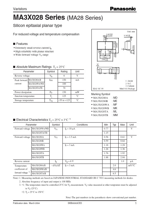
MA3X028 Series (MA28 Series)
Silicon epitaxial planar type
Unit: mm
For reduced voltage and temperature compensation ■ Features
三通道输出电源管理集成电路 MIC2827 商品说明书
MIC2827 Evaluation BoardTriple Output PMIC with HyperLight Load™ DC-DC, Two LDOs, and I 2C ControlHyperLight Load is a trademark of Micrel, Inc.MLF and Micro LeadFrame are registered trademarks of Amkor Technology, Inc.Micrel Inc. • 2180 Fortune Drive • San Jose, CA 95131 • USA • tel +1 (408) 944-0800 • fax + 1 (408) 474-1000 • General DescriptionThe MIC2827 is a three output, programmable Power Management IC. The device integrates a single 500mA PWM/PFM synchronous buck (step-down) regulator with two Low Dropout Regulators and an I²C interface that provides programmable Dynamic Voltage Scaling (DVS), Power Sequencing, and individual output Enable/Disable controls allowing the user to optimally control all three outputs.The 4MHz synchronous buck regulator features a patented HyperLight Load™ (HLL) architecture which minimizes switching losses and provides low quiescent current operation for high efficiency at light loads. Additional benefits of this proprietary architecture are low output ripple voltage and fast transient response throughout the entire load range with the use of small output capacitors, reducing the overall system size.Two high performance LDOsare integrated into the MIC2827 to provide additional system voltages for I/O, memory and other analog functions. Each LDO is capable of sourcing 150mA output current with high PSRR and low output noise. A 3% output voltage accuracy over temperature, low dropout voltage (150mV @ 150mA), and low ground current of 83uA (both LDOs operating) makes this device ideally suited for mobile applications.RequirementsThe MIC2827 Evaluation board requires at least one power supply source able to provide greater than 1A at 3V. PrecautionsThe evaluation board does not have reverse polarity protection. Applying a negative voltage to any of the input supplies or enable terminal may damage the device.The MIC2827 input and enable voltages should never exceed the voltage applied to DVIN (up to 5.5V).Getting Started1. Connect external supplies to the VIN terminals.Apply desired input voltage to the DVIN (J9) and ground (J8) terminals of the evaluation board,paying careful attention to polarity and supply voltage range (2.7V ≤ DVIN ≤ 5.5V). DVIN supplies chip VCC as well as power to the DC/DC converter. Therefore, it is required that DVIN is powered for any of the three regulators to operate properly. VIN1 (J11) provides power to LDO1 while VIN2 (J4) provides power to LDO2. Both VIN1 (J11) and VIN2 (J4) should not exceed the DVIN (J9) supply and be kept within the supply range of 1.74V ≤ VIN ≤ DVIN. An ammeter may be placed between the power supply and the input terminals of the evaluation board. Ensure that the supply voltage is monitored at the input terminals. The ammeter and/or power lead resistance can reduce the voltage supplied to the input.2. Enable/Disable the MIC2827. The MIC2827evaluation board has one enable pin for the default voltage and sequence option. The enable pin is connected to the pin terminal and due to a pull-down resistor, defaults to a low state (all outputs disabled). Alternatively, individual outputs can be enabled by software through I 2C interface. 3. Connect loads to the output terminals (J3 forLDO2, J1 for LDO1, J7 for the DC/DC converter) and GND pins (J2, J5, and J8). The load can be either passive (resistor) or active (electronic load). Be sure to monitor the output voltage at the output terminals (J1, J3, and J7). 4. Graphic user interface support (optional). TheMIC2827 Evaluation Kits includes graphical user interface software and can be used with a third party USB-to-I 2C dongle that allows configuration and testing of the MIC2827 with a standard computer. Please see the Evaluation Software section for more details.Ordering InformationPart Number Description MIC2827-B2YMT EV(DC-DC/LDO1/LDO2):1.8V/1.2V/2.8VEvaluation Kit OverviewThe MIC2827 can be operated as a standalone board or as a modular system where the evaluation board is connected to a PC via an I 2C-to-USB interface board. The MIC2827 evaluation kit includes: •MIC2827 Evaluation Board • CD-ROM including:– MIC2826/7 Evaluation Software – Evaluation User Guide Third party hardware required:• USB-to-I 2C Interface Board (dongle)• USB Peripheral CableThe USB-to-I 2C Interface Board is manufactured by Devantech and can be purchased at ( ).Connecting the Devantech USB-to-I 2C adapterWhen interfacing the MIC2827 evaluation board with the Devantech USB-to-I 2C adapter, carefully match the GND pin of the evaluation board with the GND pin of the adapter (as shown above, the USB-to-I 2C interface board will be upside down). On the MIC2827 evaluation board, the GND pin location is labeled on the right side of the board. It is the fourth pin of the jumper JP1. The Devantech USB-to-I 2C adapter has GND labeled on both sides of the interface board.MIC2826/7 Evaluation SoftwareThe MIC2826/7 evaluation software provides a Graphical User Interface (GUI) to program the MIC2827 evaluation board. A complete Application Note on the installation and operation of the MIC2826/7 Evaluation Software can be found on the installation CD under the Documents folder. The evaluation software can read and write to registers via I 2C changing output voltages, enabling/disabling outputs, and monitoring the status of the outputs.Getting Started1. Insert the MIC2826/7 Installation CD. The CDshould automatically start the installation of the MIC2826/7 software. If not, please run setup.exe in the root directory of the CD. This step may take some time and require an internet connection to update the computer to .NET Framework 3.5. 2. Install the USB-to-I 2C driver from FTDI. Theinstallation file can be found under the FTDI folder on the installation CD. Double-click on the file CDM 2.04.06.exe.3. After installing the driver, locate the virtual COMport created by the FTDI driver in the Device Manager Menu, under Ports (COM & LPT). The corresponding port will have FTDI listed as the manufacturer.4. Connect the MIC2827 to the PC via the USB-to-I2C adapter. Power the MIC2827 DVIN input.5. Open the MIC2826/7 Eval software in Programsunder the Start Menu.Evaluation SoftwareI2C Accesses ViewThe MIC2826/7 Evaluation Software has two views to control the MIC2827. The default view, shown in Figure 1, is the I2C Assesses Control View. This view gives the user direct access to the MIC2827 registers by either typing in the register number or utilizing the pull-down menu under the “Select register” section. Commands can be written to selected registers by typing the command in the Contents (hex) box and pressing the “Write” button. Similarly, reading the data of a register is accomplished by selecting the desired register and pressing the “Read” button. Please refer to the MIC2827 data sheet for details relating to the coding of the registers.MIC2827 Registers ViewThe second view, shown in Figure 2, can be found by clicking on the “MIC2827 Registers” tab. In this view, register commands are shown as buttons. By selecting a button, the command associated with the register is sent to the MIC2827. This view is separated into three sections: Status Register Bits, Enable Register bits, and the DC Voltage bits.The DC Voltage Bits utilizes pull-down menus next to the corresponding output to select the desired output voltage. After selecting the desired output voltage(s) for the corresponding output(s), selecting the “Update” button will issue the command and the output(s) will scale to the selected voltage(s).The Enable Register Bits enables and disables outputs and features of the MIC2827. By checking the box under the corresponding output, the selected output will enable. Un-checking the box will disable the selected output. Features such as Power On After Fault (POAF) and Sequence Control (SEQ CNT) can also be enabled or disabled by using their corresponding checkbox. POAF provides the option of having the outputs come back on after a fault condition is removed. A fault condition is defined as an Under Voltage Lock Out (UVLO) or Thermal Shutdown (TSD). By checking the Sequence Control box, the user turns off sequencing in Sequenced-enabled parts. In this mode, outputs start up regardless of their sequence. Please refer to the MIC2827 data sheet “Ensuring Clean Switching in Sequence-Enabled Parts” section for more details.The Status Register provides the user with an update of the status of MIC2827 outputs. If an output is above 90% of its nominal value, a red LED comes on below the corresponding output. UVLO and TSD events are also recorded in the Status Register and are cleared by clicking the “Clr” button. The Int En bit enables the IRQb output on the chip. By checking the Int En box, the IRQb output goes LOW when a UVLO or TSD event occurs.Figure 1. I2C Accesses ViewFigure 2. MIC2827 Registers View Additional InformationRipple MeasurementsTo properly measure voltage ripple on either the input or output of any regulator with a switching regulator near by, a proper ring in tip measurement is required. Standard oscilliscope probes come with a grounding clip, or a long wire with an alligator clip. Unfortunately, for high frequency measurements, this ground clip can pick up high frequency noise and erroneously inject it into the measured output ripple. The MIC2827 evaluation boards accommodate a home made ring in tip measurement by probing across input and output capacitors. This requires the removing of the oscilloscope probe sheath and ground clip from a standard oscilloscope probe and wrapping a non-shielded bus wire around the oscilloscope probe (as shown on the left). If there does not happen to be any non-shielded bus wire immediately available, the leads from axial resistors will work. By maintaining the shortest possible ground lengths on the oscilloscope probe, true ripple measurements can be obtained.Evaluation Board SchematicBill of MaterialsItem Part NumberManufacturer DescriptionQty.GRM155R61A105KE15D Murata (1) Capacitor, 1µF, 10V, X5R, 0402 size C1005X5R0J105KT TDK (2)Capacitor, 1µF, 10V, X5R, 0402 size C1, C2, C3, C5CL05A225KP5NSNC Samsung (6)Capacitor, 2.2µF, 10V, X5R, 0402 size 4GRM188R60J475K Murata (1) Capacitor, 4.7µF, 6.3V, X5R, 0603 size C1608X5R0J475M TDK (2) Capacitor, 4.7µF, 6.3V, X5R, 0603 size C6, C7CL05A475KP5NRNC Samsung (6)Capacitor, 4.7µF, 6.3V, X5R, 0402 size2 R1, R4 CRCW040210K0FKEA Vishay (3) Resistor, 10k Ω, 1%, 1/16W, 0402 size 2 R2, R3 CRCW04024K70FKEAVishay (3) Resistor, 4.7k Ω, 1%, 1/16W, 0402 size 2 JP1 0022152046Molex (4)Connector, 2.54mm (0.1”) Pitch PCB Connector, 4 pins 1 LQM21PN1R0MC0 Murata (1)) Inductor, 1.0µH, 0.8A, 2.0 x 1.25 x 0.5mm MLP2520S1R0L TDK (2) Inductor, 1.0µH, 1.5A, 2.5 x 2.0 x 1.0mm XPL2010-102ML Coilcraft (5Inductor, 1.0µH, 1.1A, 2.0 x 1.9 x 1.0mm L1CIG21W1R0MNE Samsung (6)Inductor, 1.0µH, 1.05A, 2.0 x 1.25 x 1.0mm1U1 MIC2827-xxYMT Micrel, Inc.(7) Triple Output PMIC with HyperLight Load™ DC-DC, TwoLDOs, and I 2C Control1Notes:1. Murata Tel: .2. TDK: .3. Vishay Tel: .4. Molex.: .5. Coilcraft: .6. Samsung: .7. Micrel, Inc.: .PCB Layout RecommendationsTop LayerBottom Layer。
WS2813规格书
主要特点●所有元件集成在5050封装中,不需要任何其他外围元件构成一个完整的外控像素点。
●智能反接保护,5V电源接反时不会损坏元器件。
●内置信号整形电路,任何一个像素点收到信号后经过波形整形再输出,保证线路波形畸变不会累加。
●每个像素点的三基色颜色可实现256级亮度显示,完成16777216种颜色的全真色彩显示●端口扫描频率2KHz/s。
●串行级联接口,能通过一根信号线完成数据的接收与解码。
●断点续传,额外增加一路信号线,实现双路信号传输,在单个像素点损坏的情况下,不影响整体显示效果●任意两点传传输距离在不超过5米时无需增加任何电路。
●当刷新速率30帧/秒时,级联数不小于1024点。
●数据发送速度可达800Kbps。
●光的颜色高度一致,性价比高。
主要应用领域●LED全彩发光字灯串,LED全彩软灯条硬灯条,LED护栏管。
●LED点光源,LED像素屏,LED异形屏。
产品概述WS2813是一个集控制电路与发光电路于一体的智能外控LED光源。
其外型与一个5050LED灯珠相同,每个元件即为一个像素点。
像素点内部包含了智能数字接口数据锁存信号整形放大驱动电路,防反接电路,还包含有高精度的内部振荡器和高精度恒流控制模块,有效保证了像素点光的颜色高度一致。
具有独特的断点续传功能,实现双路信号传输,在单个像素点损坏的情况下,不影响整体色彩的显示。
数据协议采用单线归零码的通讯方式,像素点在上电复位以后,DIN端接受从控制器传输过来的数据,首先送过来的24bit数据被第一个像素点提取后,送到像素点内部的数据锁存器,剩余的数据经过内部整形处理电路整形放大后通过DO端口开始转发输出给下一个级联的像素点,每经过一个像素点的传输,信号减少24bit。
像素点采用自动整形转发技术,使得该像素点的级联个数不受信号传送的限制,仅仅受限信号传输速度要求。
BIN端接收到数据信号吞噬24bit数据后,和DIN端数据比较,若DIN端无信号,BIN端有接收到信号,切换到BIN端接收输入信号,确保其中一个IC的损坏不会影响信号的级联传输,控制IC保持在BIN端口接收状态,直到断电后的下次开机重新确认。
ULN2823A中文资料
2803 THRU 2824HIGH-VOLTAGE,HIGH-CURRENT DARLINGTON ARRAYSTest Applicable Limits Characteristic Symbol Fig.DevicesTest Conditions Min.Typ.Max.Units Output Leakage CurrentI CEX1A All V CE = 50 V, T A = 25°C —< 150µA V CE = 50 V, T A = 70°C—< 1100µA 1BULx2804xV CE = 50 V, T A = 70°C, V IN = 1.0 V —< 5500µA Collector-Emitter V CE(SAT)2AllI C = 100 mA, I B = 250 µA —0.9 1.1V Saturation Voltagel C = 200 mA, I B = 350 µA — 1.1 1.3V I C = 350 mA, I B = 500 µA— 1.3 1.6V Input CurrentI IN(ON)3ULx2803x V IN = 3.85 V —0.93 1.35mA ULx2804xV IN = 5.0 V —0.350.5mA V IN = 12 V— 1.0 1.45mA I IN(OFF)4All l C = 500 µA, T A = 70°C 5065—µA Input VoltageV IN(ON)5ULx2803xV CE = 2.0 V, l C = 200 mA —— 2.4V V CE = 2.0 V, I C = 250 mA —— 2.7V V CE = 2.0 V, l C = 300 mA—— 3.0V ULx2804xV CE = 2.0 V, l C = 125 mA —— 5.0V V CE = 2.0 V, l C = 200 mA —— 6.0V V CE = 2.0 V, I C = 275 mA ——7.0V V CE = 2.0 V, l C = 350 mA——8.0V Input Capacitance C IN —All —1525pF Turn-On Delay t PLH 8All 0.5 E IN to 0.5 E OUT —0.25 1.0µs Turn-Off Delay t PHL 8All 0.5 E IN to 0.5 E OUT —0.25 1.0µs Clamp Diode I R 6All V R = 50 V, T A = 25°C ——50µA Leakage Current V R = 50 V, T A = 70°C ——100µA Clamp Diode V F7AllI F = 350 mA—1.72.0VForward VoltageComplete part number includes prefix to operating temperature range: ULN = -20°C to +85°C, ULQ = -40°C to +85°C and a suffix to identify package style: A = DIP, LW = SOIC.Types ULx2803A, ULx2803LW, ULx2804A, and ULx2804LWELECTRICAL CHARACTERISTICS at +25°C (unless otherwise noted).2803 THRU 2824HIGH-VOLTAGE,HIGH-CURRENTDARLINGTON ARRAYS115 Northeast Cutoff, Box 15036Worcester, Massachusetts 01615-0036 (508) 853-5000Test Applicable Limits Characteristic Symbol Fig.DevicesTest Conditions Min.Typ.Max.Units Output Leakage CurrentI CEX1A All V CE = 95 V, T A = 25°C —< 150µA V CE = 95 V, T A = 70°C—< 1100µA 1BULx2824xV CE = 95 V, T A = 70°C, V IN = 1.0 V —< 5500µA Collector-Emitter V CE(SAT)2AllI C = 100 mA, I B = 250 µA —0.9 1.1V Saturation Voltagel C = 200 mA, I B = 350 µA — 1.1 1.3V I C = 350 mA, I B = 500 µA— 1.3 1.6V Input CurrentI IN(ON)3ULx2823x V IN = 3.85 V —0.93 1.35mA ULx2824xV IN = 5.0 V —0.350.5mA V IN = 12 V— 1.0 1.45mA I IN(OFF)4All l C = 500 µA, T A = 70°C 5065—µA Input VoltageV IN(ON)5ULx2823xV CE = 2.0 V, l C = 200 mA —— 2.4V V CE = 2.0 V, I C = 250 mA —— 2.7V V CE = 2.0 V, l C = 300 mA—— 3.0V ULx2824xV CE = 2.0 V, l C = 125 mA —— 5.0V V CE = 2.0 V, l C = 200 mA —— 6.0V V CE = 2.0 V, I C = 275 mA ——7.0V V CE = 2.0 V, l C = 350 mA——8.0V Input Capacitance C IN —All —1525pF Turn-On Delay t PLH 8All 0.5 E IN to 0.5 E OUT —0.25 1.0µs Turn-Off Delay t PHL 8All 0.5 E IN to 0.5 E OUT —0.25 1.0µs Clamp Diode I R 6All V R = 95 V, T A = 25°C ——50µA Leakage Current V R = 95 V, T A = 70°C ——100µA Clamp Diode V F7AllI F = 350 mA—1.72.0VForward VoltageComplete part number includes prefix to operating temperature range: ULN = -20°C to +85°C, ULQ = -40°C to +85°Cand a suffix to identify package style: A = DIP, LW = SOIC. Note that the ULQ2823LW and ULQ2824LW are not presently available.Types ULx2823A, ULN2823LW, ULx2824A, and ULN2824LWELECTRICAL CHARACTERISTICS at +25°C (unless otherwise noted).2803 THRU 2824HIGH-VOLTAGE,HIGH-CURRENTDARLINGTON ARRAYS115 Northeast Cutoff, Box 15036Worcester, Massachusetts 01615-0036 (508) 853-500020Dwg. GP-070-44010080DUTY CYCLE IN PER CENT0600400O U T P U T C U R R E N T I N m A /C H A N N E L2006020Dwg. GP-070-34010080DUTY CYCLE IN PER CENT0600400O U T P U T C U R R E N T I N m A /C H A N N E L20060ALLOWABLE COLLECTOR CURRENT AS A FUNCTION OF DUTY CYCLEULx28xxLW20Dwg. GP-070-24010080DUTY CYCLE IN PER CENT 0600400O U T P U T C U R R E N T I N m A /C H A N N E L2006020Dwg. GP-070-14010080DUTY CYCLE IN PER CENT 0600400O U T P U T C U R R E N T I N m A /C H A N N E L20060ALLOWABLE COLLECTOR CURRENT AS A FUNCTION OF DUTY CYCLEULx28xxAx = Characters to identify specific device. Specification shown applies to family of devices with remaining digits as shown.2803 THRU 2824HIGH-VOLTAGE,HIGH-CURRENT DARLINGTON ARRAYSINPUT CURRENT AS AFUNCTION OF INPUT VOLTAGEULx28x3xDwg. GP-069INPUT VOLTAGE2.52.0I N P U T C U R R E N T I N m A — II N1.00.51.50.5Dwg. GP-0671.01.5COLLECTOR-EMITTER SATURATION VOLTAGE0600400C O L L E C T O R C U R R E N T I N m A200COLLECTOR CURRENT AS A FUNCTION OF INPUT CURRENT200Dwg. GP-068400INPUT CURRENT IN µA0600400C O L L E C T O R C U R R E N T I N m A200ULx28x4x6Dwg. GP-069-11012INPUT VOLTAGE52.0I N P U T C U R R E N T I N m A — I I N1.00.51.587911SATURATION VOLTAGE AS A FUNCTION OFCOLLECTOR CURRENTx = Characters to identify specific device. Characteristic shown applies to family of devices with remaining digits as shown.2803 THRU 2824HIGH-VOLTAGE,HIGH-CURRENTDARLINGTON ARRAYS115 Northeast Cutoff, Box 15036Worcester, Massachusetts 01615-0036 (508) 853-5000PACKAGE DESIGNATOR “A” DIMENSIONSDimensions in Inches (controlling dimensions)Dimensions in Millimeters (for reference only)NOTES:1.Exact body and lead configuration at vendor’s option within limits shown.2.Lead spacing tolerance is non-cumulative.3.Lead thickness is measured at seating plane or below.Dwg. MA-001-18A in19Dwg. MA-001-18A mm192803THRU2824HIGH-VOLTAGE,HIGH-CURRENT DARLINGTON ARRAYS PACKAGE DESIGNATOR “LW” DIMENSIONSDimensions in Inches(for reference only)Dimensions in Millimeters(controlling dimensions)Dwg. MA-008-18A mm1.27BSCDwg. MA-008-18A inBSCNOTES:1.Exact body and lead configuration at vendor’s option within limits shown.2.Lead spacing tolerance is non-cumulative.2803 THRU 2824HIGH-VOLTAGE,HIGH-CURRENTDARLINGTON ARRAYS115 Northeast Cutoff, Box 15036Worcester, Massachusetts 01615-0036 (508) 853-5000The products described here are manufactured under one or more U.S. patents or U.S. patents pending.Allegro MicroSystems, Inc. reserves the right to make, from time to time, such departures from the detail specifications as may be required to permit improvements in the performance, reliability, ormanufacturability of its products. Before placing an order, the user is cautioned to verify that the information being relied upon is current.Allegro products are not authorized for use as critical components in life-support devices or systems without express written approval.The information included herein is believed to be accurate and reliable. However, Allegro MicroSystems, Inc. assumes no responsi-bility for its use; nor for any infringement of patents or other rights of third parties which may result from its use.。
ICX282AQ中文资料
VDD
φRG
GND
Hφ2B
Hφ1B
NC
VL
Hφ1A
Pin Description Pin No. Symbol 1 2 3 4 5 6 7 8 9 10 11 12 Vφ4 Vφ3A Vφ3B Vφ3C Vφ2 NC NC Vφ1A Vφ1B Vφ1C GND GND Vertical register transfer clock Vertical register transfer clock Vertical register transfer clock GND GND Description Vertical register transfer clock Vertical register transfer clock Vertical register transfer clock Vertical register transfer clock Vertical register transfer clock Pin No. 13 14 15 16 17 18 19 20 21 22 23 24 Symbol VOUT VDD φRG Hφ2B Hφ1B GND NC φSUB CSUB VL Hφ1A Hφ2A Substrate clock Substrate bias∗1 Protective transistor bias Horizontal register transfer clock Horizontal register transfer clock Description Signal output Supply voltage Reset gate clock Horizontal register transfer clock Horizontal register transfer clock GND