GDB-V3三相电压变送器使用说明书
三极调节电压调节器说明书

1.5A Three Terminal Adjustable Voltage RegulatorSchematic DiagramFigure 1 · Block DiagramFeatures▪ Adjustable Output Down to 1.25V ▪ 1% Output Voltage Tolerance ▪ 0.01%/V Line Regulation ▪ 0.3% Load Regulation ▪ Min. 1.5A Output Current▪ Typical 80dB Ripple Rejection ▪ Available in Hermetic TO-257High Reliability Features – SG117A/SG117▪ Available to MIL-STD-883, ¶1.2.1▪ MSC-AMS level "S" Processing Available ▪ Available to DSCC– Standard Microcircuit Drawing (SMD) ▪ MIL-M-38510/7703405XA SG117AT-JAN ▪ MIL-M-38510/7703405YA SG117AK-JANDescription The SG117 and SG117A are 3-terminal positive adjustable voltage regulators which offer improved performance over the original 117 design. A major feature of the SG117A is a reference voltage tolerance guaranteed within ± 1%, allowing an overall powersupply tolerance to be better than 3% using inexpensive 1% resistors. Line and load regulationperformance has been improved as well.Moreover, the SG117A reference voltage is guaranteed not to exceed 2% when operating over the full load, lineand power dissipation conditions. The SG117A adjustable regulators offer an improved solution for all positive voltage regulator requirements with loadcurrents up to 1.5A.In addition to replacing many fixed regulators, theSG117/A can be used in a variety of other applicationsdue to its ‘floating’ design as long as the input -to-output differential maximum is not exceeded, such as acurrent source. A higher voltage version is available the SG117AHV and SG117HV which offers input voltage up to 60V.1.5A 3-Terminal Adjustable Voltage RegulatorConnection Diagrams and Ordering InformationConnection Diagrams and Ordering InformationConnection Diagrams and Ordering Information1.5A 3-Terminal Adjustable Voltage RegulatorAbsolute Maximum RatingsThermal DataRecommended Operating ConditionsElectrical CharacteristicsElectrical CharacteristicsUnless otherwise specified, these characteristics apply over the full operating ambient temperature for the SG117A / SG117 with -55°C < T A < 125°C, V IN– V OUT = 5.0V and for I OUT = 500mA (K, G, and IG) and I OUT = 100mA (T, and L packages). Although power dissipation is internally limited, these specifications are applicable for power dissipations of 2W for the T, and L packages, and 20W for the K, G, and IG packages.I MAX is 1.5A for the K, G, and IG packages and 500mA for the T, and L packages. Low duty cycle pulsetesting techniques are used which maintains junction and case temperatures equal to the ambient temperature.1.5A 3-Terminal Adjustable Voltage RegulatorCharacteristic CurvesFigure 2 · Output Voltage Deviation vs. Temperature Figure 3 · Output Current vs. Input / Output DifferentialFigure 4 · Adjust Current vs. Temperature Figure 5 · Input / Output Differential vs. TemperatureFigure 6 · Reference Voltage vs. Temperature Figure 7 · Quiescent Current vs. Input /OutputDifferentialCharacteristic Curves Characteristic CurvesFigure 8 · Ripple Rejection vs. Output VoltageFigure 9 · Ripple Rejection vs. FrequencyFigure 10 · Ripple Rejection vs. Output CurrentFigure 11 · Output Impedance vs. FrequencyFigure 12 · Line Transient Response Figure 13 · Load Transient Response1.5A 3-Terminal Adjustable Voltage RegulatorCharacteristic CurvesFigure 14 · Output Impedance vs. Frequency Figure 15 · Line Transient ResponseFigure 16 · Load Transient ResponseApplication InformationApplication InformationGeneralThe SG117A develops a 1.25V reference voltage between the output (OUT) and the adjust (ADJ) terminals (see Basic Regulator Circuit). By placing a resistor, R 1 between these two terminals, a constant current is caused to flow through R 1 and down through R 2 to set the overall output voltage. Normally this current is the specified minimum load current of 5mA or 10mA. It is important to maintain this minimum output load current requirement otherwise the device may fail to regulate, and the output voltage may rise.2ADJ 12REF OUT R I R R 1V V ∙++=⎪⎪⎭⎫⎝⎛Figure 17 · Basic Regulator CircuitThe I ADJ current does addan error to the output divider ratio, however because I ADJ is very small and constant when compared with the current through R1, it represents a small error and can often be ignored.It is easily seen from the above equation, that even if the resistors were of exact value, the accuracy of the output is limited by the accuracy of V REF . With a guaranteed 1% reference, a 5V power supply design, using ±2% resistors, would have a worse case manufacturing tolerance of ± 4%. If 1% resistors were used, the tolerance would drop to ± 2.5%. A plot of the worst case output voltage tolerance as a function of resistor tolerance is shown below.Figure 18 · Voltage Tolerance vs. Resistor ToleranceBypass CapacitorsInput bypassing using a 0.1 μF ceramic or 1μF solid tantalum is recommended, and especially when any input filter capacitors are more than 5 inches from the device. A 0.1µF bypass capacitor on the ADJ pin is required if the load current varie s by more than 1A/µsec. Improved ripple rejection (80dB) can be accomplished by adding a 10μFcapacitor from the ADJ pin to ground.Figure 19 · Improving Ripple Rejection1.5A 3-Terminal Adjustable Voltage RegulatorWhile the SG117 is stable with no output capacitor, for improved AC transient response and to prevent the possibility of oscillation due to an unknown reactive load, a 1μF capacitor is also recommended at the output. Because of their low impedance at high frequencies, the best type of capacitor to use is solid tantalum; ceramic capacitors may also be used. When bypass capacitors are used, it may be necessary to provide external protection diodes to prevent this external large capacitance from discharging through internal low current paths, which may damage the device. Although the duration of any surge current is short, there may be sufficient energy to damage the regulator. This is particularly true of the large capacitance on the ADJ pin when output voltages are higher than 25V. Such a capacitor could discharge into the ADJ pin when either the input or output is shorted. See figure below.Figure 20 · Use of Protection DiodesLoad RegulationBecause the SG117A is a three-terminal device, it is not possible to provide true remote load sensing. Load regulation will be limited by the resistance of the wire connecting the regulator to the load. From the data sheet specification, regulation is measured at the bottom of the package. Negative side sensing is a true Kelvin connection, with the bottom of the output divider returned to the negative side of the load. Although it may not be immediately obvious, best load regulation is obtained when the top of the divider is connected directly to the case, not to the load. This is illustrated in (Connections for Best Load Regulation). If R1 were connected to the load, the effective resistance between the regulator and the load would be:ResistanceLine Parasitic R ,R R R R P 112P =+∙⎪⎪⎭⎫⎝⎛Connected as shown, R P is not multiplied by the divider ratio. R P is about 0.004Ω per foot using 16 gauge wire. This translates to 4mV/ft. at 1A load current, so it is important to keep the positive lead between regulator and load as short as possible.Figure 21 · Connections for Best Load RegulationOUTApplication InformationCurrent LimitAs outlined in the Electrical Characteristics the current limit will activate whenever the output current exceeds the specified levels. It is also important to bear in mind that the regulator includes a foldback-current characteristic that limits the current at higher V IN to V OUT differential voltages. This power limiting characteristic will prevent the regulator from providing full output current depending on the V IN to V= differential. Also if during a short circuit situation the regulator was presented with a voltage that exceeds the Absolute Maximum Rating of 40V (e.g. V IN > 40V, V OUT = 0V) the device may fail, or be permanently damaged.Typical ApplicationsFigure 22 · 1.2V – 25V Adjustable RegulatorFigure 23 · 5V Regulator with Shut DownFigure 24 ·Figure 25 ·Programmable Current LimiterI OUT = V REF /R1** 0.8Ω ≤ R 1 ≤ 120Ω1.5A 3-Terminal Adjustable Voltage RegulatorPACKAGE OUTLINE DIMENSIONSControlling dimensions are in inches, metric equivalents are shown for general information.Figure 26 · T 3-Pin Metal Can TO-39 Package DimensionsNote:1. All exposed metalized area shall be gold plated 60 micro-inch minimum thickness over nickel plated unless otherwise specified in purchase order.Figure 27 · L 20-Pin Ceramic Leadless Chip Carrier (LCC) Package DimensionsPACKAGE OUTLINE DIMENSIONSPACKAGE OUTLINE DIMENSIONS*Excludes Weld Fillet Around Lid.Figure 28 · G/IG 3-Pin Hermetic TO-257 Package DimensionsFigure 29 · K 3-Pin TO-3 Package DimensionsMicrosemi Corporation (Nasdaq: MSCC) offers a comprehensive portfolio of semiconductor and system solutions for communications, defense & security, aerospace and industrial markets. Products include high-performance and radiation-hardened analog mixed-signal integrated circuits, FPGAs, SoCs and ASICs; power management products; timing and synchronization devices and precise time solutions, setting the world’s standard for time; voice processing devices; RF solutions; discrete components; security technologies and scalable anti-tamper products; Power-over-Ethernet ICs and midspans; as well as custom design capabilities and services. Microsemi is headquartered in Aliso Viejo, Calif., and has approximately 3,400 employees globally. Learn more at .Microsemi makes no warranty, representation, or guarantee regarding the information contained herein or the suitability of its products and services for any particular purpose, nor does Microsemi assume any liability whatsoever arising out of the application or use of any product or circuit. The products sold hereunder and any other products sold by Microsemi have been subject to limited testing and should not be used in conjunction with mission-critical equipment or applications. Any performance specifications are believed to be reliable but are not verified, and Buyer must conduct and complete all performance and other testing of the products, alone and together with, or installed in, any end-products. Buyer shall not re ly on any data and performance specifications or parameters provided by Microsemi. It is the Buyer’s responsibility to independently determine suitability of any products and to test and verify the same. The information provided by Microsemi hereunder is p rovided “as is, where is” and with all faults, and the entire risk associated with such information is entirely with the Buyer. Microsemi does not grant, explicitly or implicitly, to any party any patent rights, licenses, or any other IP rights, whether with regard to such information itself or anything described by such information. Information provided in this document is proprietary to Microsemi, and Microsemi reserves the right to make any changes to the information in this document or to any products and services at any time without notice.© 2015 Microsemi Corporation. All rights reserved. Microsemi and the Microsemi logo are trademarks of Microsemi Corporation. All other trademarks and service marks are the property of their respective owners.Microsemi Corporate Headquarters One Enterprise, Aliso Viejo, CA 92656 USAWithin the USA : +1 (800) 713-4113 Outside the USA : +1 (949) 380-6100 Sales : +1 (949) 380-6136 Fax : +1 (949) 215-4996E-mail : ***************************。
三相交流调压器说明书

KTF40A380V 三相交流调压器使用说明书单位:西安协科电子有限责任公司地址:西安市雁塔区朱雀大街88号邮编:7100612011年5月1日目录装置说明1,本装置型号意义--------------------------------------------------------1 2,技术规范-----------------------------------------------------------------1 3,工作原理-----------------------------------------------------------------2 4,装置电路图-------------------------------------------------------------4 5,控制板接口图----------------------------------------------------------5 6,装置元件布局----------------------------------------------------------6 控制板说明书--------------------------------------------------------------7一、概述----------------------------------------------------------------------7二、触发电路组成------------------------------------------------------------8三、适用装置-----------------------------------------------------------------8四、正常使用条---------------------------------------------------------------8五、主要技术参数------------------------------------------------------------8六、控制板的接线端子与参数-----------------------------------------------8七、发光二极管工作状态---------------------------------------------------10八、电位器-------------------------------------------------------------------10九、 同步输入---------------------------------------------------------------11十、 调试须知---------------------------------------------------------------11十一、控制板应用举例------------------------------------------------------11 XK104B、C在三相桥式整流电路中的应用-------------------------12XK104D在三相桥式整流电路中的应用-----------------------------13XK104B、C在三相相控调压电路中的应用-------------------------14XK104D在三相相控调压电路中的应用-----------------------------15附录A:PCB板------------------------------------------------------------16附录B:控制板接线图--------------------------------------------------17附录C:原理图-----------------------------------------------------------18模块资料-------------------------------------------------------------------19 XKMTC70AT120/180----------------------------------------------------------191,本装置型号意义:K T F-40A/380V3PH50HZ可控硅变流装置3相50Hz调压额定整流电压(V)风冷额定整流电流(A)2 技术规范:2.1 主要技术参数:a.额定输出电流: 40Ab.额定输出电压: 380Vc.负载等级: Ⅱ级 100% Idn 连续, 150%Idn 1分钟;d.冷却方式: 风冷e.主柜外形尺寸: 350×240 (长×宽)2.2 正常使用条件:本装置除了应满足GB3895-83《半导体电力变流器》、ZBK46-006-88《电化学整流器标准》外, 还应满足本产品的技术要求:a.环境温度: 户内不低于-5℃,不高于+40℃,24小时内的平均温度不超过30℃b. 空气最大相对湿度不超过90%c. 运行地点无导电及爆炸性尘埃,无腐蚀金属和破坏绝缘的气体或蒸汽。
三相三线多功能电表使用说明书

目录1. 概述2.主要功能3. 工作原理4. 规格型号5. 技术指标6. 电表的安装和接线7. 面板及符号说明8. 运输和存储9. 保证期限1. 概述电子式三相多功能电能表是采用先进的微电子技术、计算机技术和SMT制造技术,由我公司精心设计和制造的新一代电能表,它可以直接精确地测量正向、反向的有功电能以及正向和反向的无功电能,能依据相应费率和需量等要求进行处理。
并可显示当前各相电流电压及电网频率。
全部性能指标符合GB/T 17883《0.2S级和0.5S级静止式交流有功电能表》和GB/T 17215《1级和2级静止式交流有功电能表》国家标准对多功能电能表的各项技术要求,其通讯符合DL/T 645《多功能表通讯规约》的要求。
本系列产品具有四种费率、12个时段、多个时区及日时段表、百年日历时钟、红外遥控编程抄表、并具有RS485通讯接口、手动停电唤醒等功能,其性能稳定,精确度高,操作方便,是适应电能管理现代化的理想计量器具。
2. 主要功能2.1 分时计量正向有功和反向有功电能;2.2 可计量有功总电能及A、B、C分相有功电能;2.3 分时计量正向无功和反向无功电能,正向无功和反向无功计量方式可设置;2.4 分时计量正向有功、正向无功最大需量及其最大需量发生时间;2.5 可编程多个时区、费率、日时段、公共假日及多套日时段表;2.6 可实时测量各相电流、电压、功率、功率因数等参数;2.7 具有失压、失流、编程、需量清零、电池工作时间和电表运行时间等事件记录;2.8 具有历史12个月正向有功用电量记录功能;2.9 具有有功和无功测试端口,光电隔离;2.10 可通过掌上电脑非接触式(红外通讯)设表(预编程)、抄表;2.11 具有RS485远程通讯接口,通过RS485接口与PC机或掌上电脑进行通讯;2.12 可以在停电的状态下不附加任何外置直流电源进行抄表,通过红外遥控器现场查看数据;2.13 具有事件报警及故障报警功能;2.14 通过LCD显示电能表的运行状态、各种参数设置情况和各种计量数据;2.15 可实现参数自动轮显,轮显的参数(最多32项)和轮显时间、顺序可任意设置;2.16 具有编程和编程禁止功能;2.17 具有电量清零及需量复位功能;2.18 具有电量冻结、整点负荷等功能;2.19 电池更换简单容易。
V3产品使用说明

Parameter input Program no. 02 Smooth factor Trig. yTS, yTE Trig. xTE shut-off y,x Job no.: 3964 DW/OF Vel start end Vel min max Dircection X/Y Master sample 0 0,0 0,00 0,0 987654321 0/ 0 0,00 0,00 0 0,00 N mm N
评估结果, OK 或者NOK
单位
第一层 Graph
测量程序 标定压力值 压力窗口 压力位移窗口1 窗口号 位移窗口4 200,0 N
5 4
压力位移曲线
“ 曲线 ” 界面
这个曲线窗口显示压力、位移特性以及所有的公差窗口
通过 Tab(F1) 返回界面
Байду номын сангаасProg.2
通过 Hcopy(F2) 复制
1 3 2
窗口号 测量程序 (00 - 31) 最小实际值 最大实际值 最小设置值 最大设置值 Measured values : tabular form P02 wn1 wn2 wn3 wn4 wn5 wn6 wn7 wn8 OK Graph Servi F1 F2 F3 F4 Setpt Calib F5 F6 Docu F7 通过 Docu(F7) 进入文档 Docu(F7 文档界面 文档 actual values setpoint values min max min max 0,0 33,6 61,6 45,0 41,9 86,7 4,4 153,5 0,0 25,0 35,0 4,2 130,0 90,0 65,0 85,0 4,8 170,0 N N N mm N 通过 Graph(F2) 进入曲线 曲线界面 ( ) 曲线
变压器式三倍频说明书
HD-SBF三倍频发生器使用说明书武汉华新仪电力科技有限公司WuHan HuaXinyi Power Technology Co.,Ltd目录前言..................................................一、简介...............................................二、电气参数. .........................................三、操作方法...........................................四、售后服务承诺........................................五、定货须知..............................................六、注意事项..............................................前言(1)感谢您使用本公司产品,为了让您尽快熟练地操作本仪器,我们随机配备了内容详细的使用说明书,可使您获取有关产品介绍、使用方法、以及安全注意事项等各方面知识。
在第一次使用仪器之前,请务必仔细阅读,有助于您更好的使用该产品。
(2)本说明书编写时难免有错误、疏漏之处,请您多加包涵并欢迎加以指正。
(3)我们将非常感谢您能对本产品的进一步完善多提宝贵意见,以利我们将产品做得更好。
(4)因产品不断更新,本公司保留解释权。
三倍频使用说明书一、概述该产品是为了满足<<GB1094.3—85>>、<<GB1207>>和<<电气设备预防性试验规程>>—1995中三倍频感应耐压试验和局放试验而设计。
变压器、互感器感应耐压试验是检验该产品是否符合国家标准的一项重要试验。
绕组的层间、匝间、段及相间绝缘的纵绝缘感应试验,是考验绕组是否符合要求的一个重要项目。
数显三相电流电压表使用说明书.
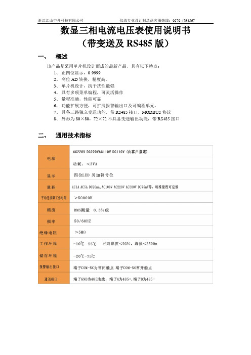
数显三相电流电压表使用说明书(带变送及RS485版)一、概述该产品是采用单片机设计而成的最新产品,具有以下特点:1、正四位显示,0-99992、高位AD转换,精度高。
3、单片机设计,抗干扰性能强4、具有多项菜单编程,可灵活操作5、量程准确,性能可靠6、功能扩展方便,可扩展报警输出口及可编程单元。
7、具备三路独立变送功能,带RS485接口,MODBUS协议8、外形为80×80,72×72不具备变送输出功能,带RS485接口二、通用技术指标三、接线图四、编程说明五、变送输出该产品具备变送输出及RS485输出。
具体操作如下:变送输出:1、首先确定仪表变送输出量程,一般可选0-20mA或4-20mA,如果需要电压信号,只需在电流输出两端并上精密电阻,输出电压精度由电阻决定。
2、第一路电流/电压对应第一路变送输出,其它二路与之类似。
3、变送输出最大值由信号量程决定,如AC5A量程,则输入电流信号为5A时对应输出20mA六、数字通讯MODBUS协议只允许在主机(PC,PLC等)和终端设备之间通讯,而不允许独立的终端设备之间的数据交换,这样各终端设备不会在它们初始化时占据通讯线路,而仅限于响应到达本机的查询信号。
主机查询:查询消息帧包括设备地址码、功能人码、数据信息码、校验码。
地址码表明要选中的从机设备;功能代码告之被选中的从设备要执行何种功能,例如功能代码03或04是要求从设备读寄存器并返回它们的内容;数据段包含了从设备要执行功能的其它附加信息,如在读命令中,数据段的附加信息有从何寄存器开始读的寄存器数量;校验码用来检验一帧信息的正确性,为从设备提供了一种验证消息内容是否正确的方法,它采用CRC16的校准规则。
从机响应:如果从设备产生一正常的回应,在回应消息中有从机地址码、功能代码、数据信息码和CRC16校验码。
数据信息码包括了从设备收集的数据:如寄存器值或状态。
如果有错误发生,我们约定是从机不进行响应。
三相无功功率监测仪表使用说明书

1概述1.1产品简介DTSD342(配置号为7Q)型三相无功功率监测仪表用于测量电网三相无功功率,它采用大屏幕LCD显示,可通过RS485进行数据采集,RS-485通信支持MODBUS-RTU和DL/T645双通信规约;具有开关量输入、输出功能。
本仪表广泛适用于变配电自动化系统、工业控制和工业自动化系统、能源管理系统和小区电力监控等场合。
1.2产品特点本仪表采用了高精度采样计量单元和高速MCU数据处理单元,可实现高精度宽范围准确计量和快速数据分析;采用段码式多行宽视角液晶显示屏,显示内容很丰富;液晶配备白色背光,可满足黑暗环境下查阅数据的要求;采用非易失存储器存储各类数据,可长时间保存数据且掉电不丢失;支持RS485通信端口和工业标准通信规约,组网便捷灵活;选配不同通信模块,可满足多种用户的不同接口需求。
2技术指标3功能介绍3.1参数测量功能本仪表可测量总和各分相无功功率。
3.2越限报警功能(1)仪表具备越限事件报警功能。
用户可从电压、电流、功率、功率因数和频率等参数中最多同时选择6个数据作为检测对象,对其设定高低限值和判断条件,当测量值越过设定的限值时报警。
仪表带有1路继电器输出,当报警参数配置为某继电器输出且该继电器为自动方式(非手动方式)时,越限报警信号就可通过该路继电器输出(继电器合闸)。
(2)仪表内部最多可同时设置6组越限报警参数。
各组越限报警参数的配置流程为:选择检测数据类别→设置检测数据阀值→设置判断条件→选择报警信号输出继电器。
①各类检测数据代码如下:(DL/T645代码为十进制数;Modbus-RTU代码为十六进制数)当检测数据代码为FF时表示该组越限报警功能关闭。
②检测数据阀值:检测数据是否越限的判断阀值。
不同的数据类型有不同的单位,如:电压—V;电流—A,有功—KW,无功—KV AR,视在—KV A,频率—Hz。
③判断条件:设置为0表示大于限额值报警;1表示小于限额值报警。
三相调压板使用说明书

说明书
技术领域
本发明是关于,对三相电源的控制方法,具体地说就是如何改变三相电源的电压的一种设备。
技术背景
在很多设备中,都不会真接使用三相电源,都要对其进行变换,包括整流设备,启动设备等,传统方法以不能满足设备对这方面的需要,所迫切需要一种更先进,更智能化的系统来控制三相电源系统。
发明内容
本发明的目的是克现有技术的缺点,提供一种更先进,更智能化的控制设备。
利用MUC 做为主控制单元,配合适当的外围电路组成的,精确,功能完善,人机界面友好的一整套控制系统。
本系统通过下述技术手段予以实现,通过精确的控制三相电源,在一个周期内导通的时间来实现电源的控制,将MUC的资源,分成不同的时间段,以实现不同的功能,系统中集成了输入、输出、A/D数据采集与数据处理功能、串行通信功能,开关量输入通道数量为4路,开关量输出通道为3路,A/D数据采集通道为2路0V—5V 10位精度,串行通信功能为RS232通信协议,可通过外接RS232转RS485实现远程通信,用户在选用时说明各功能的具体用途以便根据用途定制程序以实现各功能的配合使用,完成用户对控制系统的功能要求。
具体实施方式
本系统通过设置的四个按钮,与一个4行,16位的汉字液晶显示屏进行人机对话,对
系统的运行参数进行配置,配置好的参数存储在MUC内部的EEPROM中供系统使用时进行随时调用,系统运行时通过对照参数的配置来实时的调整运行数据,通过集成的A/D来实时的采集运行情况,并通过内部运算来调整运行状态使系统达到满意的运行效果,系统通过数字量接口来接收控制命令,输出态,与控制信息,汉字液晶显示屏同步显示运行数,当发生故障时显示故障内容,以帮助排查,系统的运行也可通过集成的四个多功能按钮,来控制启动停止与复位。
- 1、下载文档前请自行甄别文档内容的完整性,平台不提供额外的编辑、内容补充、找答案等附加服务。
- 2、"仅部分预览"的文档,不可在线预览部分如存在完整性等问题,可反馈申请退款(可完整预览的文档不适用该条件!)。
- 3、如文档侵犯您的权益,请联系客服反馈,我们会尽快为您处理(人工客服工作时间:9:00-18:30)。
1. 注意产品标签上的辅助电源信息,变送器的辅助电源等级和极性不可差错,否则将损坏变送器。 2. 变送器为一体化结构,不可拆卸,同时应避免碰撞和跌落。 3. 变送器在有强磁干扰的环境中使用时,请注意输入线的屏蔽,输出信号应尽可能短。集中安装时,最小安装间
隔不应小于 10mm。 4. 只能使用变送器的有效接线端,其它端子可能与变送器内部电路有连接,不能另图它用。 5. 当输入量超过额定值时,输出量会被限制在大约 1.2 倍额定输出值上。 6. 本系列变送器内部未设置防雷击电路,当变送器输入、输出馈线暴露于室外恶劣气候环境之中时,应注意采取
本系列部分产品采用 DIN 导轨卡装式结构,插拔式端子接线,安装、维护方便,适用于各种工控监测系统、单片 机数据采集、信号传输转换和 DCS 集散控制系统等,可广泛应用于电力、通信、铁路、矿山、冶金、交通、仪表等行 业。
二、GDB-V3 三相电压变送器选型及参数表
1、变送器型谱表
GDB 产品类型 线制代号 结构类型 输入类型
防雷措施。 7. 本产品采用阻燃 ABS 塑料外壳封装,外壳极限耐受温度为+85℃,收到高温烘烤时会发生变形,影响产品性能。
产品请勿在热源附近使用或保存,请勿把产品放进高温箱内烘烤。 8. 请勿损坏或者修改产品的标签、标志,请勿拆卸或改装变送器,否则本公司将不再对该产品提供“三包”(包换、
GDB-V3 三相电压变送器使用手册
目录:
一、变送器产品简介 二、变送器选型及参数表 三、变送器外型尺寸及端子定义图 四、主要技术指标 五、变送器的正确使用 六、注意事项
GDB-V3 三相电压变送器
使用说明书
一、GDB-V3 三相电压变送器产品简介
本系列产品采用 16 位高精度高速同步数据采集和数据处理技术、专业 MCU 控制器、特制隔离变送模块,隔离测 量三相电压的真有效值参数,并将其变换为 3 路的 0/4mA~20mA 或 0/1V~5V 标准直流信号输出。本系列产品具有 高精度、高隔离、低功耗、低漂移、温度范围宽、性能稳定、抗干扰能力强等特点。
3. 请严格按照变送器端子定义图规定连接输入输出信号,否则变送器可能会损坏或输出值会发生错误。 4. 对于需测试变送器的准确度,则应在如下条件下进行:
a) 精度为 0.05 级以上的标准信号源及 0.05 级以上的测量仪表(所用表的等级指数一定要高于产品等级指数); b) 辅助电源:标称值±0.5%,纹波≤5mV;环境温度:25℃±5℃;相对湿度:RH(45~75)%; 注:有不明处及各技术指标的试验方法请咨询我公司。
三、变送器外型尺寸图及端子定义图
1. 外型尺寸图(单位:mm)
2、变送器端子定义及接线说明示意图(具体请参照产品标签所示接线图):
注: 1、 三相电压变送器电压从可插拔端子 UA、UB、UC、UN 输入;线电压变送输出时 UN 悬空; 2、 V+为辅助电源正端,GND 为辅助电源地,与信号输出地隔离; 3、 三相电压变送器 OUT1、OUT2、OUT3 是三相相电压 UA、UB、UC 或线电压 Uab、Ubc、Uca 对应的直流信号输 出端,其地为 AGND,与辅助电源隔离;
输出类型
辅助电源
型号
说明
-□ □ □ □ □ □
V
电压变送器
3
三相
U4
4*3Pin 端子接线,35mmDIN 卡轨安装;100*114*17.5来自1交流(工频)
7
真有效电流 Iz:4~20mA
8
真有效电流 Iz:0~20mA
9
真有效电流 Iz:0~10mA
A
真有效电压 Vz:1~5V
B
真有效电压 Vz:0~10V
五、变送器的正确使用
1. 变送器的安装 本型号变送器采用标准 DIN35 导轨卡式安装,使用方便。安装方法如下: ①把变送器固定卡槽上侧勾在安装导轨上; ②旋转并使变送器下侧卡口压向卡轨,则变送器安装到卡轨上; ③从卡轨拆下时,向下拉动卡簧销并先提出下侧,即可将变送器取出;
2. 变送器出厂时,已按《产品标准》准确调定,用户连接无误后即可通电工作。接通电源后,红色 RUN 运行指示 灯应闪烁。变送器对于辅助电源没有特殊要求,多只变送器可以共用一组电源。如购买市售稳压电源时,要求 该电源的隔离电压≥2000VAC,直流输出纹波<10mV。
C
真有效电压 Vz:0~5V
T
非标准信号
3 单电源三隔离
2、变送器型号及参数表(在标准条件下测试):
GDB-V3 三相电压变送器型号及参数表(真有效值)(在标准条件下测试):
产品型号
温漂
输出类 精度等 响应 负载能
结构
(PPM/
型 x 级 时间 力
形式
℃)
GDB-V3U41x3 7~C 0.5/0.2 300mS 5mA/6V 100 U4
第2页共3页
GDB-V3 三相电压变送器使用手册
四、主要技术指标
1. 输入信号:工频,45~75Hz; 2. 输入规格:0~60V、100V、250V、400V、500V 等各量程可选; 3. 输入阻抗:电压通道≥2KΩ/V; 4. 短时输入过载能力:2 倍标称输入电压,可持续 1s; 5. 精度等级:0~5/10V 输出型±0.2%F.S,0/4~20mA 输出型±0.5%F.S; 6. 线性范围:1%~100%标称值; 7. 输出规格:0~20mA、4~20mA、0~5V、1~5V、0~10V 等标准直流信号;具体规格见产品标签; 8. 输出负载能力:电压输出型 5mA;电流输出型≤200Ω(12V 电源),≤650Ω(24V 电源); 9. 输出纹波:≤10mV(有效值,额定输出负载时); 10. 响应时间:≤300ms; 11. 隔离耐压:2500VDC,1min; 12. 环境温度:-10℃~+60℃; 13. 温度漂移:≤100PPM(-10℃~+60℃范围内) 14. 辅助电源:12VDC±10%;具体规格见产品标签; 15. 电源消耗电流:≤35mA+每通道负载电流;
电源 +24V
工作温 度(℃)
输入标称值 系列
端 子 输 入 : 0 ~ 60V 、 100V 、 -10~60
250V、400V、500V
第1页共3页
GDB-V3 三相电压变送器使用手册 注:输出信号类型 x 代码含义请参见选型表; 定货型号应包括:传感器类型、输入/输出规格(标称值)、电源、电压接线方式(三相三线与三相四线)等参数;