MLCAD软件使用手册
明锐达白板软件说明书
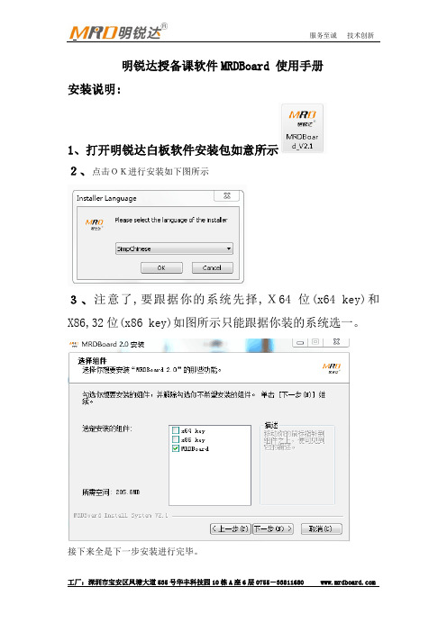
明锐达授备课软件MRDBoard 使用手册安装说明:1、打开明锐达白板软件安装包如意所示2、点击OK进行安装如下图所示3、注意了,要跟据你的系统先择,X64位(x64 key)和X86,32位(x86 key)如图所示只能跟据你装的系统选一。
接下来全是下一步安装进行完毕。
4、安装完毕后桌面上会出现这个图标为明锐达光学白板定位软件,点击进入如下图所示:设置里可以选择几点定位。
5、安装完毕后桌面上会出现这个图标,本图标为明锐达白板两边各22个快捷的服务器,会自动运行。
出厂我们以设定好,只需安装以上软件不需要设置处理能方便。
软件概述:MRDBOARD软件是一款针对课堂备课和教学开发的应用软件。
它具有界面简洁,操作简单,书写流畅等特点;可以同步展示声音,视频,flash课件,网络资源;并提供ppt标注工具和透明页标注工具方便配合原有的ppt课件教学和配合其他软件教学。
老师可在备课上课环节使用该软件可以让教学变得生动有趣,提高学习兴趣,提升教学品质。
软件工作模式:MRDBOARD软件提供编辑、全屏两种模式。
编辑模式为备课提供方便,全屏模式为上课提供方便,用户在使用过程中可以根据需要,快速切换。
编辑模式:1、编辑模式可以根据用户的喜好,隐藏或者显示菜单栏、工具栏、资源库,在工具栏上面右键弹出菜单,可设置各个部件的显示或者隐藏。
2、也可以随意调节工具栏、资源库的位置和顺序。
拖动工具栏左边区域拖动各个工具栏改变工具栏的位置,也可以拖动资源库的标题栏,移动资源库到相应的位置,下图是重新设置后的效果,用户可以根据自己的爱好随意设置界面。
全屏模式:窗口模式切换:1、编辑模式切换到全屏模式,点击工具栏中全屏模式按钮。
右上角的小衣服可以选择多项色调2、全屏模式切换到编辑模式,点击浮动工具栏右侧的编辑模式按钮。
3、全屏模式切换到电脑桌面,点击浮动工具栏左侧图标,即可切换到电脑桌面。
软件特色功能介绍:1、换肤,软件提供了六种颜色的背景的皮肤,以适应不同用户的喜好灰白界面:淡蓝界面:粉红界面:橙色界面:淡绿界面:2、透明页标注工具:3、 Ppt 标注工具:ppt 标注工具是为了配合ppt 课件教学而开发的,主要用于配合老师用ppt 进行教学。
ICP DAS PEX-P8POR8i PCI-P16POR16U 产品说明书
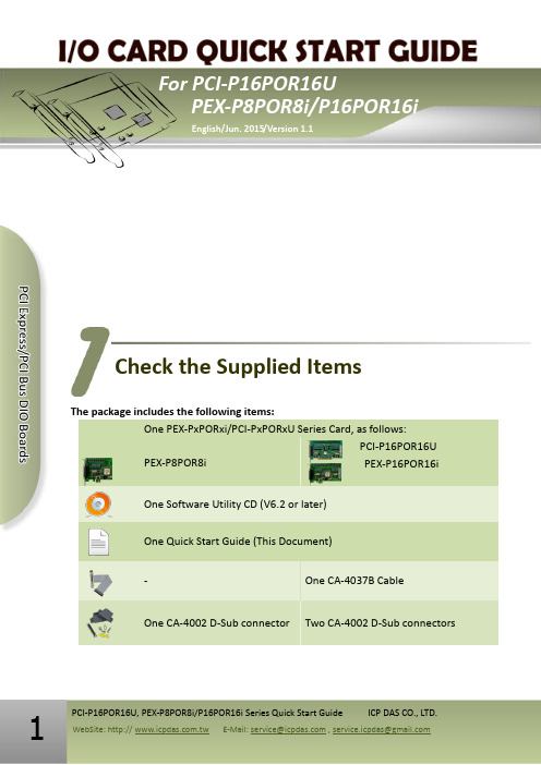
The package includes the following items:One PEX-PxPORxi/PCI-PxPORxU Series Card, as follows:PEX-P8POR8iPCI-P16POR16UPEX-P16POR16i One Software Utility CD (V6.2 or later)One Quick Start Guide (This Document)- One CA-4037B CableOne CA-4002 D-Sub connector Two CA-4002 D-Sub connectors Check the Supplied ItemsStep 1: Setup the Windows driver. The driver is located at:☐ The PISO-DIO Series classic driver supports Windows 98/NT/2K and 32-bitXP/2003/ Vista/7/8. Recommended to install this driver for have been used PISO-DIO series boards of regular user, please refer to :/pub/cd/iocard/pci/napdos/pci/piso-dio/manual/quic kstart/classic/Step 2: Click the “N ext>” button to start the installation.Step 3: Check your DAQ Card is or not on supported list, then click the “N ext>” button. Step 4: Select the installed folder, the default path is C:\ICPDAS\UniDAQ , confirm andclick the “N ext>” button.Step 5: Check your DAQ Card on list, then click the “N ext>” button. Step 6: Click the “N ext>” button on the Select Additional Tasks window. Step 7: Click the “N ext>” button on the Download Information window.Step 8: Select “No, I will restart my computer later” and then click the “F inish” button.For detailed information about the driver installation, please refer to Chapter 2.1 “Getting the UniDAQ Driver DLL Installer package ” of the UniDAQ SDK user manual.Installing the Windows Driver1. CON1/CN1: The connector for DI/O channels 0-7. Refer to Section 5 Pin Assignments.2. CON2: The connector DI/O channel 8-15. Refer to Section 5 Pin Assignments.3.SW1:Card ID function. Refer to PCI-P16R16 Series User Manual. 4. J1/JP1-JP8: Input AC or DC signals for DI 0-7. Refer to the table below. 5. J2/JP9-JP16: Input AC or DC signals for DI 8-15. Refer to the table below.6.JP2/J2:Ground Isolated Protection Jumper. Refer to PCI-P16R16 Series User Manual.7. J1: Ground Isolated Protection Jumper for PCI-P16POR16U. Refer to PCI-P16R16 Series User Manual.Please make sure input signal type jumper (J1, J2, JP1-JP8 and JP9-JP16) is kept in defaultJumper Setting❶❷❸ ❹ ❺ ❻ ❼Step 1: Shut down and power off the computer. Step 2: Remove all the covers from the computer. Step 3: Select an unused PCI Express/PCI slot. Step 4: Carefully insert your card into the PCIExpress/PCI slot and secure the board in place.Step 5: Replace the covers on the computer. Step 6: Reconnect the power supply and power onthe computer.Step 7: Once the computer reboots, follow any messages that may be displayed to complete the Plug and Play installation procedure.Step 8: Open the “Device Manager” in the Control Panel and verify that thePCI-PxPORxU/PEX-PxPORxi series card is listed correctly, as illustrated below.Installing the HardwareInstallation SuccessfulPin AssignmentsExtension Cable (CA-4037B): DB-40-Pin conversion DB-37-PinSelf-TestPrepare for device:☑One CA-3710 Cable (optional).☑DN-37 (optional) wiring terminal board.☑Exterior power supply device. For example: DP-665 (optional)Self-test wiring as follows:Step 1: Connect the DN-37 to the CON1/CN1 connector on board using the CA-3710 cable.Step 2: Connect the NO(0-7) pins to the DIA(0-7) pins.(i.e., connect the Pin1/2/3/4/5/6/7/8 to Pin12/13/14/15/16/17/18/19)Step 3: Connect the External Power Supply GND to the CM0…CM7 pins.Connect the External Power Supply GND to the GND pin.(i.e., connect the Power Supply GND to Pin20/21/22/23/24/25/26/27/29)Step 4: Connect the External Power Supply (+24 V) to the DIB0…DIB7 pins.(i.e., connect the Power Supply +24V to Pin30/31/32/33/34/35/36/37)+24VGNDExternal:Cable: CA-3710Step 5: Execute the UniDAQ Utility Program.1.In Windows 7, click the “Start”button,point to“All Programs”, and then click the“ICPDAS”folder. Point to “UniDAQDevelopment Kits”and then click the“Un iDAQ Utility”to execute the UniDAQUtility Program.2.Confirm that PCI-P16R16 Series card hasbeen successfully installed in the Hostsystem. Note that the device numbersstart from 0.3.Click the“TEST” button to start the test.Step 6: Check the results of the DIO function test.1.Click the “Digital Output” tab.2.Select “Port0” from the “Port Number” drop-down menu.3.Check the checkboxes for channels0, 2, 4 and 6.❶❸❷4. Click the “Digital Input ” tab.5. Select “Port0” from the “Port Number ” drop-down menu.6. The DI indicators will turn red when the corresponding DO channels 0, 2, 4 and 6 are ON .PEX-P8POR8i/P16POR16i and PCI- P16POR16U Series Card Product Page:/root/product/solutions/pc_based_io_board/pci/pci-p16por16.ht mlDN-37, CA-3710 and DP-665 page (optional):/products/DAQ/screw_terminal/dn_37.htm/products/Accessories/power_supply/dp-665.htm /products/Accessories/cable/cable_selection.htm Documentation and Software:CD:\NAPDOS\PCI\UniDAQ\/pub/cd/iocard/pci/napdos/pci/unidaq/Related Information❹❺❻。
NVIDIA DOCA PCC MLNX-15-060604 _v2.2.0 应用程序指南说明书
Application GuideTable of ContentsChapter 1. Introdution (1)Chapter 2. System Design (2)Chapter 3. Application Architecture (4)Chapter 4. DOCA Libraries (5)Chapter 5. Configuration Flow (6)Chapter 6. Running the Application (8)Chapter 7. Arg Parser DOCA Flags (10)Chapter 8. Port Programmable Congestion Control Register (12)8.1. Usage (12)8.2. Internal Default Algorithm (16)8.3. Counters (16)Chapter 9. References (18)Chapter 1.IntrodutionProgrammable congestion control (PCC) allows users to design and implement their own congestion control (CC) algorithm, giving them good flexibility to work out an optimal solution to handle congestion in their clusters. On BlueField-3, PCC is provided as a component of DOCA.The DOCA PCC application provides users the flexibility to manage allocation of DPA resources according to their needs. The application leverages the DOCA PCC library to generate an executable binary file.Typical DOCA application includes App running on host/Arm and App running on DPA. Developers are advised to use the host/Arm application with minimal changes and focus on developing their algorithm and integrating it into the DPA application.Chapter 2.System DesignDOCA PCC application consists of two parts:‣Host/Arm app is the control plane. It is responsible for allocating all resources and handover to the DPA app initially, then destroying everything when the DPA appfinishes its operation. The host app must always be alive to stay in control while the device app is working.‣Device/DPA app is the data plane. It is mainly for CC event handler. When the first thread is activated, DPA App initialization is done in the DOCA PCC library by calling the algorithm initialization function implemented by the user in the app. Moreover, the user algorithm execution function is called when a CC event arrives. The user algorithm takes event data as input and performs a calculation using per-flowcontext and replies with updated rate value and a flag to sent RTT request.The host/Arm application sends command to NIC firmware when allocating or destroying resources. CC events are generated by NIC hardware automatically when sending data or receiving ACK/NACK/CNP/RTT packets, then the device application handles these eventsSystem Designby calling the user algorithm. After the DPA application replies to hardware, handling of current event is done and the next event can arrive.Chapter 3.Application Architecture/opt/mellanox/doca/applications/pcc/src├── host│ ├── pcc.c│ ├── pcc_core.c│ └── pcc_core.h└── device├── algo│ ├── rtt_template.h│ ├── rtt_template_algo_params.h│ ├── rtt_template_ctxt.h│ └── rtt_template.c└── pcc_dev_main.cThe main content of the reference DOCA PCC application files are the following:‣host/pcc.c – entry point to entire application‣host/pcc_core.c – host functions to initialize and destroy the PCC application resources, parsers for PCC command line parameters‣device/pcc_dev_main.c – callbacks for user CC algorithm initialization, user CC algorithm calculation, algorithm parameter change notification‣device/algo/* – user CC algorithm reference template. Put user algorithm code here.Chapter 4.DOCA LibrariesThis application leverages the following DOCA libraries:‣DOCA PCC libraryChapter 5.Configuration Flow1.Parse application argument.a).Initialize arg parser resources and register DOCA general parameters.doca_argp_init();b).Register PCC application parameters.register_pcc_params();c).Parse all registered parameters.doca_argp_start();i.Parse DOCA flags.ii.Parse DOCA PCC parameters.2.PCC initialization.pcc_init();a).Open DOCA device that supports PCC.b).Create DOCA PCC context.c).Configure affinity of threads handling CC events.3.Start DOCA PCC.doca_pcc_start();a).Create PCC process and other resources.b).Trigger initialization of PCC on device.c).Register the PCC in the NIC hardware so CC events can be generated and anevent handler can be triggered.4.Process state monitor loop.doca_pcc_get_process_state();doca_pcc_wait();a).Get the state of the process:Configuration Flowb).Wait on process events from the device.5.PCC destroy.doca_pcc_destroy();a).Destroy PCC resources. The process stops handling PCC events.b).Close DOCA device.6.Arg parser destroy.doca_argp_destroy();Chapter 6.Running the Application1.Refer to the following documents:‣NVIDIA DOCA Installation Guide for Linux for details on how to install BlueField-related software.‣NVIDIA DOCA Troubleshooting Guide for any issue you may encounter with the installation, compilation, or execution of DOCA applications.‣NVIDIA DOCA Applications Overview for additional compilation instructions and development tips of DOCA applications.2.The pre-built PCC binary is located under /opt/mellanox/doca/applications/pcc/ bin/doca_pcc. To build all the applications together, run:cd /opt/mellanox/doca/applications/meson /tmp/buildninja -C /tmp/build3.To build only the allreduce application:a).Edit the following flags in /opt/mellanox/doca/applications/meson_options.txt:‣Set enable_all_applications to false‣Set enable_pcc to trueb).Run the commands in step 2.Note: doca_pcc is created under /tmp/build/pcc/src/.4.Pre-run setup:a).Enable USER_PROGRAMMABLE_CC in mlxconfig:mlxconfig -y -d /dev/mst/mt41692_pciconf0 set USER_PROGRAMMABLE_CC=1b).Reset firmware or power cycle the host.5.Running the application on the host or BlueField, CLI example:/opt/mellanox/doca/applications/pcc/bin/doca_pcc -d mlx5_0Application usage:Usage: doca_pcc [DOCA Flags] [Program Flags]DOCA Flags:-h, --help Print a help synopsis-v, --version Print program version information-l, --log-level Set the log level for the program <CRITICAL=20, ERROR=30, WARNING=40, INFO=50, DEBUG=60>Running the ApplicationProgram Flags:-d, --device <IB device names> IB device name that supports PCC(mandatory).-w, --wait-time <PCC wait time> The duration of the DOCA PCC wait(optional), can provide negative values which means infinity. If not provided then -1 will be chosen.-p, --pcc-threads <pcc-threads-list> A list of the PCC threads numbers to be chosen for the DOCA PCC context to run on (optional). Must be provided as astring, such that the number are separated by a space.For additional information on available flags, use -h:/opt/mellanox/doca/applications/pcc/bin/doca_pcc -h6.To run doca_pcc using a JSON file:doca_pcc --json [json_file]For example:cd /opt/mellanox/doca/applications/pcc/bin./doca_pcc –-json ./pcc_params.jsonChapter 7.Arg Parser DOCA Flags Refer to NVIDIA DOCA Arg Parser Programming Guide for more information.Arg Parser DOCA FlagsChapter 8.Port ProgrammableCongestion ControlRegisterThe Port Programmable Congestion Control (PPCC) register allows the user to configure and read PCC algorithm parameters.It supports the following functionalities:‣Enabling different algorithms on different ports‣Querying information of both algorithms and tunable parameters/counters‣Changing algorithm parameters without compiling and reburning user image‣Querying or clearing programmable counters8.1. UsageThe PPCC register can be accessed using a string similar to the following:sudo mlxreg -d /dev/mst/mt41692_pciconf0 -y --get --op "cmd_type=0" --reg_name PPCC --indexes "local_port=1,pnat=0,lp_msb=0,algo_slot=0,algo_param_index=0"sudo mlxreg -d /dev/mst/mt41692_pciconf0 -y --set "cmd_type=1" --reg_name PPCC --indexes "local_port=1,pnat=0,lp_msb=0,algo_slot=0,algo_param_index=0"Where you must:‣Set the cmd_type and the indexes‣Give values for algo_slot, algo_param_index‣Keep local_port=1, pnat=0, lp_msb=0‣Keep doca_pcc application running8.2. Internal Default AlgorithmThe internal default algorithm is used when enhanced connection establishment (ECE) negotiation fails. It is mainly used for backward compatibility and can be disabled using "force mode". Otherwise, users may change doca_pcc_dev_user_algo() in the device app to run a specific algorithm without considering the algorithm negotiation.The force mode command is per port:sudo mlxreg -d /dev/mst/mt41692_pciconf0 -y --get --op "cmd_type=2" --reg_name PPCC --indexes "local_port=1,pnat=0,lp_msb=0,algo_slot=15,algo_param_index=0"sudo mlxreg -d /dev/mst/mt41692_pciconf0.1 -y --get --op "cmd_type=2" --reg_name PPCC --indexes "local_port=1,pnat=0,lp_msb=0,algo_slot=15,algo_param_index=0"8.3. CountersCounters are shared on the port and are only enabled on one algo_slot per port. The following command enables the counters while enabling the algorithm according to the algo_slot:sudo mlxreg -d /dev/mst/mt41692_pciconf0 -y --set "cmd_type=1,counter_en=1" --reg_name PPCC --indexes "local_port=1,pnat=0,lp_msb=0,algo_slot=0,algo_param_index=0"After counters are enabled on the algo_slot, they can be queried using cmd_type 0xC or 0xD.sudo mlxreg -d /dev/mst/mt41692_pciconf0 -y --get --op "cmd_type=12" --reg_name PPCC --indexes "local_port=1,pnat=0,lp_msb=0,algo_slot=0,algo_param_index=0"sudo mlxreg -d /dev/mst/mt41692_pciconf0 -y --get --op "cmd_type=13" --reg_name PPCC --indexes "local_port=1,pnat=0,lp_msb=0,algo_slot=0,algo_param_index=0"Chapter 9.References ‣/opt/mellanox/doca/applications/pcc/srcNoticeThis document is provided for information purposes only and shall not be regarded as a warranty of a certain functionality, condition, or quality of a product. NVIDIA Corporation nor any of its direct or indirect subsidiaries and affiliates (collectively: “NVIDIA”) make no representations or warranties, expressed or implied, as to the accuracy or completeness of the information contained in this document and assume no responsibility for any errors contained herein. NVIDIA shall have no liability for the consequences or use of such information or for any infringement of patents or other rights of third parties that may result from its use. This document is not a commitment to develop, release, or deliver any Material (defined below), code, or functionality.NVIDIA reserves the right to make corrections, modifications, enhancements, improvements, and any other changes to this document, at any time without notice.Customer should obtain the latest relevant information before placing orders and should verify that such information is current and complete.NVIDIA products are sold subject to the NVIDIA standard terms and conditions of sale supplied at the time of order acknowledgement, unless otherwise agreed in an individual sales agreement signed by authorized representatives of NVIDIA and customer (“Terms of Sale”). NVIDIA hereby expressly objects to applying any customer general terms and conditions with regards to the purchase of the NVIDIA product referenced in this document. No contractual obligations are formed either directly or indirectly by this document.NVIDIA products are not designed, authorized, or warranted to be suitable for use in medical, military, aircraft, space, or life support equipment, nor in applications where failure or malfunction of the NVIDIA product can reasonably be expected to result in personal injury, death, or property or environmental damage. NVIDIA accepts no liability for inclusion and/or use of NVIDIA products in such equipment or applications and therefore such inclusion and/or use is at customer’s own risk.NVIDIA makes no representation or warranty that products based on this document will be suitable for any specified use. Testing of all parameters of each product is not necessarily performed by NVIDIA. It is customer’s sole responsibility to evaluate and determine the applicability of any information contained in this document, ensure the product is suitable and fit for the application planned by customer, and perform the necessary testing for the application in order to avoid a default of the application or the product. Weaknesses in customer’s product designs may affect the quality and reliability of the NVIDIA product and may result in additional or different conditions and/or requirements beyond those contained in this document. NVIDIA accepts no liability related to any default, damage, costs, or problem which may be based on or attributable to: (i) the use of the NVIDIA product in any manner that is contrary to this document or (ii) customer product designs.No license, either expressed or implied, is granted under any NVIDIA patent right, copyright, or other NVIDIA intellectual property right under this document. Information published by NVIDIA regarding third-party products or services does not constitute a license from NVIDIA to use such products or services or a warranty or endorsement thereof. Use of such information may require a license from a third party under the patents or other intellectual property rights of the third party, or a license from NVIDIA under the patents or other intellectual property rights of NVIDIA.Reproduction of information in this document is permissible only if approved in advance by NVIDIA in writing, reproduced without alteration and in full compliance with all applicable export laws and regulations, and accompanied by all associated conditions, limitations, and notices.THIS DOCUMENT AND ALL NVIDIA DESIGN SPECIFICATIONS, REFERENCE BOARDS, FILES, DRAWINGS, DIAGNOSTICS, LISTS, AND OTHER DOCUMENTS (TOGETHER AND SEPARATELY, “MATERIALS”) ARE BEING PROVIDED “AS IS.” NVIDIA MAKES NO WARRANTIES, EXPRESSED, IMPLIED, STATUTORY, OR OTHERWISE WITH RESPECT TO THE MATERIALS, AND EXPRESSLY DISCLAIMS ALL IMPLIED WARRANTIES OF NONINFRINGEMENT, MERCHANTABILITY, AND FITNESS FOR A PARTICULAR PURPOSE. TO THE EXTENT NOT PROHIBITED BY LAW, IN NO EVENT WILL NVIDIA BE LIABLE FOR ANY DAMAGES, INCLUDING WITHOUT LIMITATION ANY DIRECT, INDIRECT, SPECIAL, INCIDENTAL, PUNITIVE, OR CONSEQUENTIAL DAMAGES, HOWEVER CAUSED AND REGARDLESS OF THE THEORY OF LIABILITY, ARISING OUT OF ANY USE OF THIS DOCUMENT, EVEN IF NVIDIA HAS BEEN ADVISED OF THE POSSIBILITY OF SUCH DAMAGES. Notwithstanding any damages that customer might incur for any reason whatsoever, NVIDIA’s aggregate and cumulative liability towards customer for the products described herein shall be limited in accordance with the Terms of Sale for the product.TrademarksNVIDIA, the NVIDIA logo, and Mellanox are trademarks and/or registered trademarks of Mellanox Technologies Ltd. and/or NVIDIA Corporation in the U.S. and in other countries. The registered trademark Linux® is used pursuant to a sublicense from the Linux Foundation, the exclusive licensee of Linus Torvalds, owner of the mark on a world¬wide basis. Other company and product names may be trademarks of the respective companies with which they are associated.Copyright© 2023 NVIDIA Corporation & affiliates. All rights reserved.NVIDIA Corporation | 2788 San Tomas Expressway, Santa Clara, CA 95051。
Smart ADM CAIXA CAIXA CAIXA CAIXA 操作员手册说明书
Manual de Uso Básico do Sistema SmartADM CAIXA CAIXA CAIXA CAIXA Operador 1 2 3 4 5 Senha 1 2 3 4 5- Abertura de caixa.1°Clicar 2x no ícone “Smart Genius” (Lâmpada) na tela inicial do computador.2° Colocar Operador e Senha, de caixa.Obs: Para a primeira vez da abertura do sistema no dia, colocar o suprimento (dinheiro inicial da gaveta) e repetir a senha de caixa usada.- Entrada e Saída de Caixa.Para entrar ou tirar dinheiro do caixa.Na tela de Atendimento.1° Apertar CTRL.2° Escolher opção “Entrada/Saída do Caixa”3° Usar operador e senha de ADM.4° Colocar Motivo.5° Selecionar o Tipo (Entrada/Saída).6° Clicar 2x no campo “Dinheiro”.7° Digitar valor.8° Clicar em “OK”Na tela de Atendimento.1° Apertar “CRTL”.2° Escolher a opção “Cadastro de Produtos”.3° Usar operador e senha de ADM.4° Apertar “F1 – Novo”.5° Passar o Código do produto em “Código”.OBS: Se for produto sem código de barras, utili zar o códigoque o sistema gerar.6° Preencher “Descrição”. (Nome do Produto)7° Preencher “R$ Custo”.8° Preencher “R$ Venda”.9° Selecionar unidade de medida do produto, “Unidade”.10° Preencher o “Estoque”.11° Ir para a aba “Tributação”, como marcado abaixo.12° Preencher “NCM”.OBS: Para pesquisar o NCM clicar em “Consulta NCMPIS/COFINS”.13° Selecionar a “Alíquota ECF”.14° Selecionar a “Categoria”.15° Clicar em “F2 – Salvar”.OBS: Informações sobre Alíquota e Categoria são passadas pelo escritório de contabilidade.Para alterar um cadastro, na tela de Cadastrar Produto, apertar F3 para Pesquisar o Produto, ou, escrever o nome do produto no campo “Pesquisa” ou passar o código dele no campo “Código”.Na tela de Atendimento.1° Apertar “CRTL”.2° Escolher a opção “Cadastro de Clientes”.3° Usar operador e senha de ADM.4°“F1 – Novo”.5° Preencher “Nome”.6° Escrever demais campos do cliente.OBS: A cidade deve ser pesquisada com o botão “F6”.7° Selecionar “Formas de Pagamento”.8° Clicar em “F3 – Salvar”.Para alterar um cliente já cadastrado, na tela de “Cadastro de Clientes”, apertar o botão “F2 – Pesquisar “.- VendasPrincipais Botões:F1 Finalizar Venda.F2 Pesquisar o Cliente.F3 Pesquisar o Produto.F4 Alterar quantidade de um produto apenas.F5 Cancelar um produto do atendimento.F6 Estornar ultima venda.F9 Contas a receber.Na tela de Atendimento.1° Pressionar F3 – Pesquisar produto ou passar o código de barras do produto no com o leitor no campo “Produto”.2°Depois de passar todos os produtos seguir para finalização,F1 – Finalizar Venda.3° Escolher o método de pagamento.4° Seguir com a forma de pagamento desejada até o f im do processo.- Conferencia do CaixaNa Tela Inicial do sistema.Clicar em Movimento do Caixa.Para conferir todas as vendas passadas pelo caixa e valores em caixa. Clicar em “Visualizar Saldo”.- Fechamento do sistemaPara fechar o sistema e qualquer outra tela,seguir pressionando a tecla “ESC” no teclado.。
清华山维软件说明书(11-12章)

菜单启动:文件 -〉打开 ESP 工作空间 功能描述:打开指定目录下的 ESP 工作空间。 1.选择 ESP 工作空间存放路径; 2.点击打开。
11.6 保存ESP工作空间
功能启动: ○1 菜单启动:文件 -〉保存ESP工作空间 ○2 工作空间菜单启动:鼠标右键 -〉保存 功能描述:将当前工作空间内的编辑进行保存。
菜单启动:文件 -〉输入输出 -〉输出外部数据 功能描述:直接读取 EPS 系统的数据。 1.选择输出数据的格式; 2.选择输出调入数据文件所在的路径;
11.20 调入外部数据
菜单启动:文件 -〉输入输出-〉调入外部数据 功能描述:直接读取 EPS 系统以外的各种格式的数 据。将线、面类型数据转成编码为 1 的线,将点类型数 据转成编码为 0 的点,原图形的形状保留,原图形的图 层、颜色保留,原图形的其它基本属性转到临时扩展属 性表中。 一般用于数据分析或数据转换,在做数据转换方案 时提供数据分析。通过这种方式,可以不使用数据的原 始系统将数据打开。 1.选择原始数据的格式; 2.选择调入数据文件所在的路径; 3.选中文件名后,打开,即可将该数据调入。
图 11-12 调入外部数据格式
11.21 打印区域设置
功能启动:
105
清华山维·软件说明书
○1 菜单启动:文件 -〉打印区域设置
○2 工作空间菜单启动:快捷工具栏 -〉 功能描述:设置打印范围、打印比例,打印效果等打印出图的参数。 页面方案: 打印页面设置的方案,系统中默 认的有标准正分幅图和带状斜分幅图两种;用户可 以点按钮 添加或 删除方案。 图纸:即选纸,用户可以选择系统默认的纸张也可
11.12 调入EXF格式数据
本功能的对话框 菜单启动:文件-〉输入输出 -〉 调入 EXF(1.0,2.0) 功能描述:将 EPS 的 EXF 格式 的数据文件添加到本系统。添加 EXF1.0 或 2.0 版的数据,1.0、2.0 为版本号系统自动识别版本。如图 11-7。 1.选择 EXF 文件所在的路径。 2.选择要引入的 EXF 文件,打 开,即可将该数据调入。
qcad使用手册

qcad使用手册
QCAD使用手册
QCAD是一款优秀的二维CAD绘图软件,具备良好的用户界面和强大
的功能,广泛应用于建筑设计、机械制图等行业。
本手册将从菜单设置、绘图技巧、命令使用等方面进行详细介绍,帮助使用者更好地掌
握软件操作。
一、菜单设置
QCAD的菜单设置包括工具栏、状态栏、菜单栏等。
在工具栏上,我
们可以通过简单的拖拽将常用命令加入到工具栏中,方便平时的操作。
状态栏可以显示当前画布的信息,如缩放比例、鼠标位置等。
而菜单
栏则包含了软件的所有功能,可以通过菜单栏的快捷方式进行操作。
二、绘图技巧
QCAD的绘图技巧包括坐标系设置、图层设置、线型设置、填充效果
设置等。
在绘图时,我们需要先设置好坐标系,确定绘图的起点和终点,以便后续的操作。
同时,图层设置可以让我们将不同的图形分别
绘制在不同的图层上,便于后期的编辑和修改。
对于线型和填充效果
的设置,则可以让我们的图形更具美感和表现力。
三、命令使用
QCAD的命令使用包括基本命令、编辑命令、快捷指令等。
基本命令
包括线段、圆弧、多边形等绘图指令,而编辑命令包括移动、旋转、
缩放等操作。
同时,QCAD支持快捷指令,通过键盘输入命令和参数,可以快速完成操作,提高工作效率。
总之,QCAD是一款非常优秀的二维CAD软件,具备方便的用户界面
和强大的功能。
通过本手册的介绍,相信使用者已经掌握了一些基本
的绘图技巧和命令使用方法,可以更加顺利地完成各种绘图工作。
德威课件制作软件录播系统用户手册
德威课件制作软件用户手册目录一、德威录播大师flv版 (1)1. 软件介绍 (1)2. 软件特点 (1)更轻量级的课件 (1)更自动化 (1)专业级辅助功能 (1)更强兼容性 (2)3. 安装与卸载 (2)运行环境 (2)部署建议 (3)安装 (3)卸载 (3)4. 软件授权 (4)5. 详细指南 (4)德威屏幕搜集 (4)德威录播大师 (6)启动/停止录制 (14)课件播放 (14)二、德威录播大师PPT版 (15)1. 产品描述 (15)2. 产品特点 (16)3. 产品功能 (16)4. 安装与卸载 (16)安装 (16)卸载 (16)5. 软件授权 (17)6. 创建课程 (17)7. 选择视频源 (19)8. 录制三分屏 (20)9. 查看课件 (21)三、德威课件大师 (22)1. 软件介绍 (22)2. 软件特点 (23)3. 安装与卸载 (23)安装 (23)卸载 (23)系统环境 (23)软件授权 (23)软件版本 (23)网校三分屏课件制作套餐 (24)4. 操作指南 (24)合成视频+PPT课件 (24)合成视频+DOC课件的专门的地方 (29)编辑课件 (31)时刻点编辑 (31)目录名称编辑 (32)编辑课件信息 (32)修改课件logo (33)视频区域添加图片 (34)修改版权图片 (34)打包课件 (35)更多合成任务 (35)三、问题反馈 (36)四、技术支持 (38)一、德威录播大师flv版1. 软件介绍德威录播大师EZCam 是一款简单、易用、高清课程实时录制系统, 它能够轻松地将教学中的音视频场景、讲稿等。
内容录制为一体化的三分屏课件并实时直播,录制操作支持全自动化。
录制出的课件文件小、音质好、画面清楚,是学校积存课程资源的最正确伴侣,也是企业E-Learning 的好帮手,更是培训机构的上佳选择。
2. 软件特点更轻量级的课件a.屏幕图像和鼠标行为别离捕捉,能有效减小课件大小b.可设置抓屏的颜色位数,可使课件最小化更自动化录制启停自动化:启动、停止一键弄定专业级辅助功能1)可设定台标:支持透明台标2)可输入字幕:支持转动字幕3)可插入片头片尾:可插入图片或视频、动画类型的内容作为片头和片尾更强兼容性课件录制生成的视频格式为通用的flv,格式,兼容与windows系统,电话及平板电脑等硬件环境。
matra mhs 29c532e edac 用户手册说明书
29C532E 1. DescriptionThe 29C532E EDAC is a very low power bus-watch 32-bit Error Detection And Correction unit (EDAC). EDAC is used in a high integrity system for monitoring and correcting data values coming from the memory space. Such a bus-watch EDAC is connected as a peripheral on the data bus and watches on and controls the integrity of the data memory.During a processor write cycle, at each memory location (32-bit width), EDAC calculated checkword (7 or 8-bit width) is added. When performing a read operation from memory, the 29C532E verifies the entire checkword and data combination. It detects and can correct 100% of all the single-bit errors and it detects all multi-bit errors but can not correct them. All the errors are reported to the master system to allow the processor to take action as required. In case of single-bit error, the Correctable ERRor flag is set and the single-bit in error is complemented (corrected). Then, the data can be substituted to the corrupted data on the system data bus. In case of multi-bit error, the Non-Correctable ERRor flag is set, the data can not be repaired. Note that when multi-bit errors occur, there are some bit patterns which may appear as possible correctable errors. Therefore, if the environment produces this type of error, the EDAC must be used in detect-only-without-correction configuration. Data and syndrome analysis must be rapidly done.Because the 29C532E latches the data, byte or 16-bit word write operations are possible if they take place in a read-modify-write accesses to the memory space. When the 29C532E uses 7-checkbit, it can detect any errors on any single 1 or 4-bit memory chip. The 8-checkbit option gives the additional capability to detect all errors on any 8-bit memory chip.2. FeaturesD32-bit Operation (7 or 8 Check Bits)D Bus Watch ArchitectureD Fast Error Detection: 32 nsD Fast Error Correction: 39 nsD Corrects All Single-Bit ErrorsDetects All Double-Bit ErrorsDetects Some Multi-Bit ErrorsDetects Chip Error (x1, x4 & x8 RAM Format)D Correctable and Non-Correctable Error Flags D Very Low Power CMOSD TTL CompatibleD Single 5V ± 10% Power SupplyD High Drive Capability on Bus: 12.8 mAD100-Pin Multi-Layer Quad Flatpack32-Bit Bus-Watch EDACError Detection And Correction unit查询29C532E供应商捷多邦,专业PCB打样工厂,24小时加急出货29C532E 3. Interface3.1. Block DiagramSYNCHK29C532E 3.2. Pin ConfigurationIndex CornerDOE [29C532E 3.3. Pin Description29C532EAll I/O and I buffers have a pull-up resistor '100 Ω.29C532E4. Checkbit GenerationThe checkbit generator produces 8 checkbits (whatever N39 value) from the incoming data DI [31..0] according the following table.Table 1:Checkbit generation (x indicates bit of D [31..0] used in the parity calculation)ExampleTo create GCB [3], bit 31, 30, 27, 23, 22, 19, 15, 14, 13, 12, 10, 9, 8, 7, 4 and 0 of DI [31..0] are 3ORed together.If SRAM devices 1 or 4-bit are used in a memory system controlled by the 29C532E EDAC, it is only necessary to store 39 bits (D [31..0] & C [6..0]).If SRAM devices 8-bit are used in a memory system controlled by the 29C532E EDAC, 40 bits (D [31..0] & C [7..0]) must be stored.29C532E 5. Syndrome GenerationThe syndrome generator produces 8 syndrome-bits (whatever N39 value) from the incoming data DI [31..0] and the associated checkbit RCB [7..0] (via CI [7..0] or DIA [7..0] following DIAG [1] value) according the following table. Table 2:Checkbit generation (x indicates bit of D [x1..0] used in the parity calculation)29C532ETable 2:(continue)The syndrome bit SY[x] is the XOR of the received checkbit RCB[x] and the parity calculation on DI [31..0]. Example:To create SY [1], bit 30, 28, 25, 24, 20, 17, 16, 15, 13, 12, 9, 8, 7, 6, 4 and 3 of DI [31..0] are NXORed together. Then, the result is XORed with the associated checkbit RCB [1] of the checkbit byte read at the same address than the data word DI [31..0].If SRAM devices 1 or 4-bit are used in a memory system controlled by the 29C532E EDAC, only 39 bits (D [31..0] & C [6..0]) are checked and the generated syndrome word is 7-bit width.If SRAM devices 8-bit are used in a memory system controlled by the 29C532E EDAC, 40 bits (D [31..0] & C [7..0]) are checked, the generated syndrome word is 8-bit width.6. Syndrome DecodingThe syndrome decoder generates the error flags CERR (Correctable ERror) and NCERR (Non-Correctable ERror). It mainly provides corrected data word to the system bus if a correctable error occurs.In case of single bit-error, using the syndrome value, this block decodes which bit is in error and complements it to correct the data word. This correction is only made on the 32 bits of data not on the checkbit word.The inputs of the syndrome decoder are:D the 32 bits of data coming from the system data bus,D the syndrome coming from the syndrome generator,D the control signal N39. N39 signal controls if 39 or 40 bitswill be decoded from the entire word.29C532E Table 3:7-bit syndrome word to bit-in-error (N39=1)Note:N.E.D=No Error Detected,D [x]=Data bit–in–error,C [x]=Check bit–in–error=Multi–bit–in–error29C532ETable 4:8-bit syndrome word to bit-in-error (N39=0)Note :N.E.D=No Error Detected,D [x]=Data bit–in–error,C [x]=Check bit–in–error=Multi–bit–in–error29C532E 7. 7-Bit Syndrome WordThis feature is available when the N39 pin is driven at ahigh level.7.1. No ErrorIf there is no error in the read data or checkbit, all thesyndrome word is ”00”. The EDAC flags are inactive.7.2. Single Bit-In-ErrorWhen the Memory Data word (D [31..0] & C[6..0]) read has one bit-in-error, the 20C532E EDAC develops a code (syndrome) which indicates the bit in error (each bit have its own syndrome value). In this case, the syndrome decoder sets low the correctable error flag CERR, but NCERR flag remains at high level.In case of single bit-error on D [31..0], if the control lines SYNCHK = non active and CORRECT = active, the corrected value (CDO [31..0]) is available on DO [31..0] internal bus and the syndrome word is available on CO [6..0]. The corrected value is obtains to complement the bit-in-error.In same conditions, if a single bit-error occurs on C [6..0], the corrected value of the checkbit is not available in the device.Table 5:7-bit syndrome word for single bit-error.7.3. Double Bit-In-ErrorWhen the Memory Data word (D [31..0] & C[6..0]) read has two bit-in-error, the 20C532E EDAC develops a syndrome different of 0x00. The syndrome value generated by a double bit-in-error never takes place of a syndrome value generated by a single bit-in-error. In this case, the syndrome decoder sets low the non correctable error flag NCERR and CERR flag remains at high level. Example :If data D [12] and D [9] are incorrect, syndrome bit SY [5] and SY [0] are set to one (SY= 0x21), NCERR flag is set low (CERR flag remains at high level).7.4. Triple Bit-In-ErrorWhen the Memory Data word (D [31..0] & C[6..0]) read has three bit-in-error, the 20C532E EDAC develops a syndrome different of 0x00. The syndrome value generated by a triple bit-in-error can have any value, even a syndrome value normally generated by a single29C532Ebit-in-error. NCERR flag or CERR flag can be activated following the value of the generated syndrome.Example :If data D [28], D [18] and D [1] are incorrect, syndrome bit SY [6], SY [5] and SY [1] are set to one (SY= 0x62),NCERR flag is set low (CERR flag remains at high level).Fault example :If data D [24], D [12] and D [3] are incorrect, syndrome bits SY [4..0] are set to one (SY= 0x1F). The syndrome is decoded by the 29C532E EDAC has being a correctable error on D [4]. Then, CERR flag is set low and NCERR flag remains at high level. A correction would cause more errors.7.5. Multi Bit-In-ErrorWhen the Memory Data word (D [31..0] & C[6..0]) read has four or more bit-in-error, the 20C532E EDAC develops a non controlled syndrome. This syndrome can take any value, from 0x00 (No Error Detected) to specific syndrome value of single bit-in-error .Example :If the data read = 0x00000000 instead of 0xFFFFFFFF,the generated syndrome is 0x00. Then, no error flag is actived.7.6. 4-Bit Wide Memory ErrorThe 7 checkbit code can be used to provide error detection for up to four errors occuring in the following fields:D D [31..28],D D [27..24],D D [23..20],D D [19..16],D D [15..12],D D [11..8],D D [7..4],D D [3..0],D C [6..4],DC [3..0].The 29C532E EDAC can flag any number of errors in 4-bit wide memory chip. If the one device returns from one to four bit-in error, the CERR and NCERR flags are generated following the error type and the generated syndrome takes a value which never overlaps the code of a single bit-in-error. This is a restriction to triple and multi bit-in-error.Example :If the device controlling D [23..20] generates error, the 15possible codes are different of 0x00 and of those describing a single bit-in-error.8. 8-Bit Syndrome WordThis feature is available when the N39 pin is driven at a low level.8.1. No ErrorIf there is no error in the read data or checkbit, all the syndrome word is ”00”. The EDAC flags are inactive.29C532E 8.2. Single Bit-In-ErrorWhen the Memory Data word (D [31..0] & C[7..0]) read has one bit-in-error, the 20C532E EDAC develops a code (syndrome) which indicates the bit in error (each bit have its own syndrome value). In this case, the syndrome decoder sets low the correctable error flag CERR, but NCERR flag remains at high level.In case of single bit-error on D [31..0], if the control lines SYNCHK = non active and CORRECT = active, the corrected value (CDO [31..0]) is available on DO [31..0] internal bus and the syndrome word is available on CO [7..0]. The corrected value is obtains to complement the bit-in-error.In same conditions, if a single bit-error occurs on C [7..0], the corrected value of the checkbit is not available in the device.Table 6:8-bit syndrome word for single bit-error.8.3. Double Bit-In-ErrorWhen the Memory Data word (D [31..0] & C[7..0]) read has two bit-in-error, the 20C532E EDAC develops a syndrome different of 0x00. The syndrome value generated by a double bit-in-error never takes place of a syndrome value generated by a single bit-in-error. In this case, the syndrome decoder sets low the non correctable error flag NCERR and CERR flag remains at high level. Example:If data D [24] and D [3] are incorrect, syndrome bit SY [7, 2, 0] are set to one (SY= 0x85), NCERR flag is set low (CERR flag remains at high level).8.4. Triple Bit-In-ErrorWhen the Memory Data word (D [31..0] & C[7..0]) read has three bit-in-error, the 20C532E EDAC develops a syndrome different of 0x00. The syndrome value generated by a triple bit-in-error can have any value, even a syndrome value normally generated by a single bit-in-error. NCERR flag or CERR flag can be activated following the value of the generated syndrome. Example :If data D [25], D [20] and D [6] are incorrect, syndrome bit SY [5, 4, 2, 1, 0] are set to one (SY= 0x37), NCERR flag is set low (CERR flag remains at high level).Fault example: If data D [30], D [15] and D [0] are incorrect, syndrome bits SY [7, 5, 3, 2] are set to one (SY= 0xAC). The syndrome is decoded by the 29C532E EDAC has being a correctable error on D [14]. Then, CERR flag is set low and NCERR flag remains at high level. A correction would cause more errors.8.5. Multi Bit-In-ErrorWhen the Memory Data word (D [31..0] & C[7..0]) read has four or more bit-in-error, the 20C532E EDAC develops a non controlled syndrome. This syndrome can take any value, from 0x00 (No Error Detected) to specific syndrome value of single bit-in-error .Example:If the data read = 0x00000000 instead of 0xFFFFFFFF, the generated syndrome is 0x00. Then, no error flag is actived.29C532E8.6. 4-Bit Wide Memory ErrorThe 8 checkbit code can be used to provide error detection for up to four errors occuring in the following fields:D D [31..28],D D [27..24],D D [23..20],D D [19..16],D D [15..12],D D [11..8],D D [7..4],D D [3..0],D C [7..4],D C [3..0].The 29C532E EDAC can flag any number of errors in 4-bit wide memory chip. If the one device returns from one to four bit-in error, the CERR and NCERR flags are generated following the error type and the generated syndrome takes a value which never overlaps the code of a single bit-in-error. This is a restriction to triple and multi bit-in-error.Example :If the device controlling D [7..4] generates error, the 15 possible codes are different of 0x00 and of those describing a single bit-in-error.8.7. 8-Bit Wide Memory ErrorThe 8 checkbit code can be used to provide error detection for up to eight errors occuring in the following fields:D D [31..24],D D [23..16],D D [15..8],D D [7..0],D C [7..0].The 29C532E EDAC can flag any number of errors in 8-bit wide memory chip. If the one device returns from one to eight bit-in error, the CERR and NCERR flags are generated following the error type and the generated syndrome takes a value which never overlaps the code of a single bit-in-error. This is a restriction to triple and multi bit-in-error.29C532E 9. Transactions9.1. ControlThe controller guides The data flow in the 29C532E EDAC. This data flow control defines the value of the output buses DO [31..0] & CO [7..0] and the checkbit bus RCB [7..0]:D SYNCHK and CORRECT control flow on DO [31..0], D OLE/CHK and DIAG [0] control flow on CO [7..0], D DIAG [1] controls flow on RCB [7..0].Table 7:Data Flow ControlEight signals are used to supervise the transactions :D DOE [3..0] control Data Output Buffers, D COE control Checkbit Output Buffer.D OLE/CHK controls Data Output Latch,D ILE controls Checkbit and Data Input Latchs, D DLE controls Diagnostic Input Latch.29C532E9.2. Memory WriteNCERRCERRDOE [3..0]D [31..24]D [23..16]D [15..8]D [7..0]ILEC [7..0]DLE DIAG [1]N39CORRECT DIAG [0]SYNCHK OLE/CHKCOE29C532E9.3. Memory Read ... Till Error GenerationCERR NCERRD [31..24]D [23..16]D [15..8]D [7..0]ILEC [7..0]DLE DIAG [1]N39CORRECT DIAG [0]SYNCHK DOE [3..0]COEOLE/CHK29C532E9.4. Memory Read (continue)... With Correction - Single Bit-in-errorD [31..24]D [23..16]D [15..8]D [7..0]ILEC [7..0]DLE DIAG [1]N39CORRECT DIAG [0]SYNCHK OLE/CHK DOE [3..0]COENCERRCERR (*) when OLE/CHK = H, then CO [7..0] = SY [7..0] (placed in schematic),when OLE/CHK = I, then CO [7..0] = GCB [7..0]29C532E9.5. Byte Memory Write - Read Modify WriteA) 32-bit Data Memory + Checkbit ReadIn In In InInDOE [3..0]D [31..24]D [23..16]D [15..8]D [7..0]ILEC [7..0]COE DLE DIAG [1]CERR NCERRN39SYNCHK CORRECT OLE/CHK DIAG [0]29C532EB) Preparing of 32–bit Corrected DataIn In In InInDOE [3..0]D [31..24]D [23..16]D [15..8]D [7..0]ILEC [7..0]COE DLE DIAG [1]CERR NCERRN39SYNCHK CORRECT OLE/CHK DIAG [0]29C532ED [7..0]C) 8-bit Data Memory + Checkbit WriteIn-Out In-Out In-Out In Out29C532E 10. Signal Timing 10.1. Memory Write29C532E 10.2. Memory Read29C532E10.3. Memory Read With CorrectionD [31..0]CORRECTC [7..0]ILEDOE [3..0]COEOLE/CHKCERRNCERR29C532E10.4. Memory Byte Write (Read Modify Write)D [31..8]ILE D [7..0]C [7..0]DOE [0]DOE [2..0]COEOLE/CHKCERRNCERRThe information contained herein is subject to change without notice. No responsibility is assumed by TEMIC for using this publication and/or circuits described herein : nor for any possible infringements of patents or other rights of third parties which may result from its use.。
- 1、下载文档前请自行甄别文档内容的完整性,平台不提供额外的编辑、内容补充、找答案等附加服务。
- 2、"仅部分预览"的文档,不可在线预览部分如存在完整性等问题,可反馈申请退款(可完整预览的文档不适用该条件!)。
- 3、如文档侵犯您的权益,请联系客服反馈,我们会尽快为您处理(人工客服工作时间:9:00-18:30)。
第二十四届中国儿童青少年威盛中国芯计算机表演赛3D创意搭建赛建议软件(MLCAD)操作指南MLCAD操作指南1.下载MLCAD及运行环境...................................- 2- 2.安装运行MLCAD软件.....................................- 5- 3.使用MLCAD软件........................................ - 7-3.1 零件区的使用................................... - 9 -3.2 工具栏的使用...................................- 14- 4.创意搭建赛作品保存.................................... - 20-第二十四届中国儿童青少年威盛中国芯计算机表演赛全国组委会制作提供1.下载MLCAD及运行环境(LDraw)●输入网站的网址(),进入网站的主页面,在该页面中找到“Get Started”选项,点击进入“Get Started”,如下图。
●在“Get Started”页面中下载LDraw系列软件:在这个界面中提供了支持多种操作系统的LDraw系列软件的安装文件下载,点击Windows 操作系统的安装文件。
进入新界面后点击“Step 1”下面的“LDraw_AIOI_2014-01_setup_32bit_v2.zip”安装文件,输入验证码并下载LDraw软件,如下图所示。
下载完成后再进入网页,在“Download”选项下选择“Download”,出现下图所示的界面;●点击上图所示的最下面的“MLCAD”,进入到图一所示的界面,然后按图示点击进入到图二所示的界面;图一图二●从上图中左侧工具条中点击“Download”,出现下图所示的界面,然后点击“Download the latest version V3.40 now(1.1MB)”下载MLCAD 主程序。
2.安装运行MLCAD软件将下载好的LDraw软件进行解压,并双击进入到安装页面。
●点击“Next”按步骤完成安装。
安装可能会花费很长的时间,请耐心等待。
●安装完LDraw后,解压并进入下载好的“MLCad_V3.40”文件。
双击MLCAD(红色的图标)就进入到MLCAD程序制图的界面了。
3.使用MLCAD软件●如下图所示为使用 MLCAD软件设计模型时的完整界面,分为菜单栏、工具栏、零件库、状态栏、操作栏和模型搭建区。
●上述7个区域的基本功能如下:⏹菜单栏下拉式菜单提供了各种各样的功能;✧File----文件菜单,具有打开和保存文件,保存模型的图片,导出文件,打印文件等;✧Edit—编辑菜单,提供了多种编辑和修改功能;✧Navigate—在查看模式下,对模型搭建步骤进行定位,选择需要查看的步骤;✧Veiw—查看零件的状态,以及工具栏的使用状态;✧Multipart—对文件中出现的多个模型进行操作,例如新建子模型、导入导出模型、删除模型等等;✧Extras—提供各种附加功能、生成功能、文件缓冲功能、微小零件合成功能等等;✧Settings—用来对MLCAD的模式、视图等进行设置;✧Help—打开帮助对话框,帮助用户解决各种问题。
⏹工具栏 10个工具栏,几十种工具可供使用;这些工具栏可以根据需要打开或者关闭,按照下图所示,选择菜单栏上的View菜单中的Toolbars选项,就会出现下图所示的下拉菜单,在需要的工具栏选项前面打勾就可以打开该工具栏,取消某个工具栏前面的勾就会关闭该工具栏。
✧零件库分类清楚的零件库中有几千种零件,能够满足搭建各种复杂模型的需要;✧状态栏本质上也是一个工具栏,但是它不提供操作的功能,只是自动显示鼠标的坐标,以及零件库中鼠标所指的零件的编号和名称;✧操作栏显示了在模型搭建区中添加每个零件,以及进行所有的操作盒命令;模型搭建区有4个可以调整大小的视窗,可以显示模型的3视图和立体视图,给模型的而搭建带来极大地便利。
在设计模型时,只需要从零件区选择你所需要的零件,使用鼠标拖拽到搭建区,按照你的搭建想法进行摆放。
在 CAD软件中,设计模型就像在现实空间中搭积木一样简单!当然,在你完全熟悉各部分的具体使用细节之前,你可能会觉得不那么得心应手。
别着急!以下将详细介绍每一部分的具体使用方法。
3.1 零件区的使用MLCAD的零件库由零件列表窗口和零件预览窗口组成,在零件列表窗口中,所有的零件根据名称和属性分成了6类:Brick、Baseplate、Electric、echnic、Train、Plate,其他不能够并入这6大类的零件全部汇总入Other Parts。
零件库列表窗口(1)零件库列表窗口(2)零件库预览窗口打开某一类别的目录,就可以看到很多的同类零件按照名称整齐的排列着,零件预览窗口可以显示零件的形状,让人有一种直观的认识,见上图。
通常我们在寻找零件的时候,都是现在零件列表窗口中确定零件的大致位置,然后在零件预览窗口中选中需要的零件。
另外,也通过零件预览窗口中的类别下拉菜单选择零件类别(图一)。
零件预览窗口有两种模式:一种是显示的零件尺寸较小、精度较低,但是同时显示很多的零件(图二),另一种显示的零件尺寸较大、精度较高,但是同时显示的零件数量也变少很多(图三)。
两种模式可以通过在窗口中点击鼠标右键来相互切换,并且当你将鼠标指在某个零件上,状态栏就会显示零件的编号和名称。
图一图二图三如果在搭建模型的过程中,找不到所需的零件,那么就可以采用搜索的方法,在零件列表窗口中点击鼠标右键,弹出一个菜单,选中最上面的Find 选项,在弹出的如下图所示的对话框中输入零件的名称或者编号进行搜索。
通常搜索零件采用的都是搜索编号的方法。
因为一般情况下使用MLCAD都是为了保存已经存在的模型,而在每个真实的乐高零件上面都有零件编号,所有输入零件的编号,都可以很快的找到需要的零件。
接下来就分别介绍零件库中各个类别的零件,一边大家在使用的时候能很快的找到自己所需要的零件。
1)Brick\块类零件这类零件是乐高积木中最简单、最古老的种类,在20世纪30年代乐高积木诞生的时候,就只有这类零件。
块状零件虽然大小不一,形状各异,但是有一个共同的特性:这类零件除了可以通过顶部的突点和底部的凹槽与其他零件连接之外,没有其他的连接方式(少数特殊的零件也是在基本的块状零件基础上变化出来的)。
2)Baseplate\基板类零件这类零件都是各种各样的平板,是在搭建乐高模型的时候作为基础使用的。
通常它们都比较的大,最小的也有8*12最大的可以达到50*50,多数的基板上都有图案,可以适应不同的需要,例如搭建与交通相关的模型,可以选择带有道路图案的羁绊;搭建与自然景观有关的模型,可以选用带有河流、湖泊图案的基板。
3)Electric\带电零件乐高零件中所有的与电有关的零件都归到这一类中,其中常用的E友RCX、马达、传感器、导线、电池盒。
4)Technic\技术零件这类零件主要是所有乐高零件中最重要的一类,搭建比较复杂的机械装置、机器人时,都需要用这类来搭建外部结构和机械转动。
常用的零件有:梁、轴、齿轮、滑轮、连接件、销、气泵、活塞等等。
5)Train\火车零件这类零件主要是乐高的一个重要的系列产品——火车系列中的零件。
其中具有代表性的零件有:铁轨、火车底盘、车厢、铁路信号灯、栏杆等等。
6)Plate\板类零件这类零件的主体都是板,虽然有很多并不是很规则的板,有不部分都带有其他的结构。
其中要说明的是,这类板与前文提到的基板有很大的不同的,一方面零件的面积要比基板小的多,最小的是1*1,最大的也只不过10*10;另外,基板只有上面的突点可以和其他零件连接,底部并没有凹槽。
7)Other Parts\其他零件所有不属于以上6类的零件,都被归类到这里面。
这些零件中的大多数一般都不太会使用,但是其中有两种确实经常要使用的,它们是轮子和轮胎。
3.2工具栏的使用下面将详细介绍10个工具栏中工具的功能:1)主工具栏主工具栏中的一些常用工具,例如:新建文件、保存文件、复制、剪切、粘贴等等,在此就不多做介绍了,主要介绍一下两个工具:✧Save Images…打开一个保存图像对话框,通过一些简单设置可以保存模型当前的图像或者搭建模型的步骤图;✧Save Parts List…打开一个对话框,保存搭建模型所使用的所有零件的列表,包含零件的编号、名称、颜色和数量等信息。
2)模式工具栏模式工具栏是对MLCAD做基本设置的工具栏,提供了多种模式设置工具,熟练的掌握各种模式之间的切换和设置,是搭建MLCAD模型的基础。
✧View Mode 选择查看模式模型搭建区内的模型自动变成适合视窗的大小,但是这时无法对零件进行操作,只能查看模型的搭建步骤(前提是需要添加步骤);✧Edit Mode 选择编辑模式,可以向模型搭建区中添加零件,或者对模型上的零件进行操作;✧Pan Mode 选择拖动模式,可以通过鼠标拖动模型在视窗中的位置,使模型处于便于编辑的位置;✧Zoom Mode 选择缩放模式,可以通过鼠标的上下拖动改变任意一个视窗中模型的大小而不影响其他视窗中的模型大小;✧Grid Coarse 选择粗网格,在模型搭建区中隐藏着不可见的网格,网格可以帮助零件定位,网格的基本单位为乐高基本单位的1|20,粗网格在X-Y-Z(零件的长、高、宽三个方向),三个方向上的尺寸分别是10-8-10;✧Grid Medium 选择中网格,网格的尺寸为5-4-5;✧Grid Fine 选择细网格,网格的尺寸为1-1-1;✧Draw To Selection Only 选择这个工具,视窗中只会显示被选中零件以及它之前添加到模型上的零件,而将其后加入的零件隐藏。
3)缩放工具栏缩放工具栏的功能非常简单,仅仅用来改变模型在视窗中的而大小,前9中工具(从6%到300%)是按照比例来缩放模型,并且4个视窗中的模型比例相同;最后一种工具是自动将模型缩放到全部可以容纳进视窗的大小,4个视窗中模型的比例可以不同。
4)对象工具栏该工具栏中工具的作用都是往操作栏中添加对象,这些对象包括零件、命令、步骤、背景等等。
这些对象加入后会自动在操作栏中添加一个操作,这个操作的添加位置是你选中的操作后面。
✧Add Part…选择该工具可以打开一个添加零件对话框,通过在按照零件编号顺序排列的零件列表中选择需要的零件添加到模型中;✧Add Comment…打开添加命令对话框,输入所需要的命令,添加在操作栏中被选中的对象的后面;✧Add Step…在被选中的对象后面添加一个步骤;✧Add Rotation Step…打开添加旋转步骤对话框,在选中的对象后面添加的一个旋转步骤,该步骤可以显示模型任意的角度;✧Add Rotation End Step…在选中的对象后面添加一个做末端旋转的步骤;✧Add Step Background…打开添加步骤背景对话框,为模型的步骤图添加背景;✧Add Clear Statement…在选中的对象后面添加一个清除控制,当查看到该控制之后的步骤时,该控制之前的零件会被全部清除(只是不显示出来,并不是被删除);✧Add Buffer Exchage…在选中的对象后面添加一个缓冲器。