XILINX-时序约束使用指南中文
Vivado集成开发环境时序约束介绍

Vivado时序约束本文主要介绍如何在Vivado设计套件中进行时序约束,原文出自Xilinx中文社区。
1Timing Constraints in Vivado -UCF to XDCVivado软件相比于ISE的一大转变就是约束文件,ISE软件支持的是UCF(User Constraints File),而Vivado软件转换到了XDC(Xilinx Design Constraints)。
XDC主要基于SDC(Synopsys Design Constraints)标准,另外集成了Xilinx的一些约束标准,可以说这一转变是Xilinx向业界标准的靠拢。
Altera从TimeQuest开始就一直使用SDC标准,这一改变,相信对于很多工程师来说是好事,两个平台之间的转换会更加容易些。
首先看一下业界标准SDC的原文介绍:Synopsys' widely-used design constraints format, known as SDC, describes the "design intent" and surrounding constraints for synthesis, clocking, timing, power, test and environmental and operating conditions. SDC has been in use and evolving for more than 20 years, making it the most popular and proven format for describing design constraints. Essentially all synthesized designs use SDC and numerous EDA companies have translators that can read and process SDC.Xilinx原先的自成一派(UCF)其实其实也算做的不错,相信使用过UCF的工程师也有同感,并没有什么不便。
xilinx fpga中时钟输入管脚的约束

xilinx fpga中时钟输入管脚的约束在Xilinx FPGA中,时钟输入管脚的约束是非常重要的,它们可以确保时钟信号的稳定性和一致性,从而保证设计的性能和可靠性。
因此,合理设置时钟输入管脚的约束是进行FPGA设计中不可忽视的一部分。
时钟输入管脚约束主要包括以下几个方面:1.频率约束:时钟输入管脚的频率约束指定了该管脚接收的时钟信号的频率范围。
在设计中,需要根据时钟源的特性和系统的工作要求来设置合适的频率约束。
2.总线延迟约束:在一些应用中,时钟信号可能需要进行时序约束,以确保各个时钟域之间的同步稳定性。
总线延迟约束指定了时钟信号与其他信号的最大传播延迟,这样可以避免时序问题和死锁。
3.约束路径的设置:时钟输入管脚的约束路径设置是确保时钟信号按照设计要求正确到达目标寄存器的关键。
通过设置约束路径,可以规定时钟信号到达目标寄存器的最长路径,确保时钟信号的稳定性,减少时钟抖动和时钟周期不稳定等问题。
4.时钟输入和输出约束:时钟输入管脚还可能有一些其他的约束设置,如时钟输入和输出的相位约束、时钟输入和输出的组合约束等。
这些约束的目的是保证时钟信号的稳定性和相位一致性。
除了上述的基本约束外,还有一些特殊的约束需要注意:1.编译工具约束:在进行FPGA设计时,可以使用Xilinx的编译工具对设计进行优化和约束分析。
通过正确设置时钟输入管脚的约束,可以使编译工具更好地理解设计的时钟域和时序要求,从而提高设计的性能和可靠性。
2.时钟插入延迟约束:在一些高速设计中,时钟插入延迟约束非常重要。
它指定了时钟信号从输入管脚到达目标寄存器之间的最小插入延迟。
通过设置时钟插入延迟约束,可以在设计中引入适当的延迟,从而使时钟信号的到达时间更加可控和稳定。
3.锁定时钟约束:在一些需要时钟同步的设计中,可能需要设置锁定时钟约束。
这个约束规定了时钟信号之间的相位关系,确保它们在设定的相位范围内保持同步。
这对于一些高速通信和信号处理系统中的数据同步非常重要。
xilinx官方论坛解释时序约束

Timing ConstraintsFollowing along the forum traffic, it has come to may attention that timing constraints are often a mystery to new users. In order to help those who have never had to constrain their timing, I offer the following part one, of five parts, on timing constraints.Some BasicsTiming constraints apply to nets or networks, the path or paths taken from one element to all of the inputs of subsequent elements. One can also call out a specific path that is part of a net or network.Every design should have at least one period constraint that specifies the clock and the duty cycle of the clock. A clock is always required for synchronous design, and so the period constraint is the most basic and is always a required constraint for any design. If there is more than one clock, each requires its own period constraint.The period constraint will define how all nets must be routed in order to meet the timing requirements for proper operation.A group may be defined to generically refer to many nets or paths of a selected set, such as a bus or control group.PriorityWhen it comes to having many constraints for a design the following applies: the more general the constraint, the lower its priority, and, conversely, the more specific a constraint, the higher the priority.For example, a period constraint on a clock net or network is very general and will be over-ruled by a from:to constraint on a specific net or network.The specific constraint for the from:to (or from:thru:to) is deemed more important than the more general constraint for any net within a clock domain.There is a timing specification interaction report (the .tsi report) that details how the constraints interact. Select this option in the timing analyzer for reporting if you have a set of constraints, and you need to know how they are interacting and which priorities have been set.One can override the assumed priorities and manually set the priority of any timing constraint. The use of the priority command allows setting a very low priority, such as 0, or even a negative priority, such as -10, which will be evaluated with an even higher priority than 0.Example 1The PERIOD constraint only covers nets from Synchronous Elements to Synchronous Elements, such as FFS to FFS, as shown in blue below:NET "clk20" TNM_NET = “tnm_clk20";TIMESPEC "TS_clk20" = PERIOD “tnm_clk20" 20 ns HIGH 50 %;A TIMEGRP (timing group) is created called tnm_clk20 which contains all of the downstream synchronous components that net clk20 drives. All of the paths between these synchronous elements are then constrained with the timing specification TS_clk20, which specifies a 20 ns requirement from synchronous element to synchronous element and a HIGH 50% (clk20 has a 50/50 duty cycle).Example 2FROM:TO constraints are used to define a requirement for paths that go between two groups.TIMESPEC TS_my_fromto = FROM my_from_grp TO my_to_grp 40 ns;tells the tools that you need to ensure that data makes it from the components in the timing group ‘my_from_grp’ to ‘my_to_grp’ in 40 ns. Timing Analyzer will still calculate the clock skew from source group to destination group, but at a lower priority (if the clocks are related). Predefined groups can be used, for example:TIMESPEC TS_F2F = FROM FFS TO FFS 40 ns;If we need leave out the time unit (ns, ps, etc…), then the tools presume ns:TIMESPEC TS_P2P = FROM PADS TO PADS 30;You can leave FROM or TO off of the constraint and make it more generic:TIMESPEC TS_2P = TO PADS 40;All of the FROM:TO constraints in the examples above would be of higher priority than the PERIOD constraint.TSI ReportThe TSI report is generated with the ‘-tsi design.tsi’ switch in the TRCE command line, or by specifying the option in the timing analyzer. If a user does not see a path under the correct constraint, this is the best place to start. This report will also make suggestions on ways toimprove constraints in the universal constraints file (UCF). This report will also notify the user of any paths that are constrained by multiple clock domains:Example 3Constraint Interaction Report=============================Constraint interactions for TS_clk0_1 = PERIOD TIMEGRP "clk0_1" TS_clk HIGH 50%;1 paths removed by TS_my_fromto = MAXDELAY FROM TIMEGRP "my_to_grp" TO TIMEGRP "FFS" 40 ns;Analysis of Example 3In other words, the FROM:TO constraint (just one) was applied ahead (higher priority) of the PERIOD constraint.Following along the forum traffic, it has come to my attention that timing constraints are often a mystery to new users. In order to help those who have never had to constrain their timing, I continue with part 2 (of 5) on timing constraints.Setup and HoldIn a practical synchronous digital system, the data must arrive before the clock edge that samples it. The minimum amount of time in which the data must arrive before the clock edge is called the setup time.As well as arriving before the clock edge, the data must persist for some finite amount of time at the clock edge. This is called hold time. Hold time may be negative, zero, or positive. When it is negative, the data goes away before the clock edge. When it is zero, the data persists until the clock edge. When it is positive, the data persists for some time after the clock edge.By design, in the FPGA fabric, for all speed grades, all hold times are either negative or zero. This simplifies the placement and routing, as the data only needs to arrive before the clock edge, and is allowed to change immediately following a clock edge. The value that the data exceeds the minimum setup time is known as slack. Slack should always be positive. If a report shows a negative slack, then the setup timing will be inadequate (data will arrive too late).The clock path itself has delay, or skew. Thus, to analyze the timing, the tools will calculate the arrival time of the data and the clock at the flip-flop of interest. ConstraintsIf you recall from last time, the period constraint defines the clock period for the synchronous elements of interest (the flip-flops). The timing analyzer verifies that all paths between synchronous elements meet the setup and hold timing for your design. A violation of a period constraint will appear in the timing report, and have a negative slack value. It will either be identified as violating a setup requirement or a hold requirement.If a setup requirement has been violated, then the data needs to arrive at the flip-flop sooner. To do so may require a faster path. If the place and route software cannot find a faster path, you do have the option of placing the path manually in the FPGA_Editor tool, but this is a tool of last resort. It is better to try to re-architect the circuit to meet the requirement. One way to do this is to place a flip-flop earlier in the path. This is known as pipe-lining, and will add latency to the signal, but it will also allow the value to be captured properly.If a hold requirement has been violated (the data went away before the clock edge arrived), then this is often an indication that you have a design problem (bad architecture). Values should only change on the clock edge, and not before. If an external value is changing before the clock edge, one needs to delay the clock edge (using a DCM or PLL) so that the data is now registered properly by the new delayed clock.An alternative is to use the Idelay element in the IOB to move the data to where the clock is valid.Data Valid WindowThe time from before the clock edge (setup) plus the time after the edge (hold) is known as the data valid window, or the time the data must be stable to be properly registered. If the data is not valid for at least this amount of time, then the results are indeterminate, or unknown.MetastabilityJust because the data was not valid for as long as required does not mean that the output of the flip-flop is metastable--metastable is different from indeterminate! An output could be 0 or 1, seemingly at random, if the timing is not met. Metastability means the edge was “almost” capable of capturing the state and the flip-flop output is in some intermediate state (not 1, not 0) for some time after the clockedge. Metastability cannot be prevented, as it is a fact of the physics of the circuits, if the clock edge and the data are almost perfectly “missed.”In a properly designed synchronous system there are no problems with metastability. Metastability is a problem when something is asynchronous, like pressing a key on a keyboard, or when two synchronous clocks are asynchronous to each other. When something is asynchronous, it needs to be synchronized.For how to deal with metastability, please consult:/class/ee183/handouts_spr2003/synchronization_pres.pdfNext time: Tprop, or offsets.Following along the forum traffic, it has come to may attention that timing constraints are often a mystery to new users. In order to help those who have never had to constrain their timing, I continue with part 3 (of 5 parts) on timing constraints.Tprop or OffsetThe time it takes to get a signal from point A to point B is called the propagation time. It is based on the speed of light through a medium. For example, a trace on a printed circuit board carries signals at around 6 to 7 picoseconds per millimeter. Finding this time can be done by running simulations or solving equations when you know the dielectric constant for the material and the geometry of the wiring traces. Inside the silicon device the signals behave in much the same way, but also may be delayed by going through active circuits (buffers, inverters, logic and interconnect).Often, you can also measure these times with the help of an oscilloscope. Propagation times generally do not vary much at all when the path has no active elements. If the path is in silicon, the strength of the transistors will cause the path delay to vary with both a maximum value and a minimum value. Timing needs to be met for both, obviously.In order to tell the tools when data arrives at a particular location, offset constraints are used.OFFSET_INThe OFFSET IN constraint defines the relationship of a clock and data as they enter the device:OFFSET = IN 2 ns VALID 16 ns BEFORE “clk20";This constraint tells the tools that data will be setup at PADs 2 ns before the clk20 rising edge, and that the data will remain valid for 16 ns after it arrives. This constraint only applies to PADs that go to registers that are clocked by clk20, or a derivative of clk20 (a derived constraint).OFFSET requires a PERIOD constraint on clk20, so that it understands the clocking structure. This following is also acceptable:OFFSET = IN 2 ns BEFORE “clk20";However, the above statement will not check the hold time because we do not know when the data goes away at the PIN of the FPGA. If the data will not be setup until 2 ns after the clock edge, then we use the following:OFFSET = IN -2 ns VALID 16 ns BEFORE “clk20"; # Do not use OFFSET IN AFTER(the text after the # is a comment)OFFSET_OUTThe OFFSET OUT constraint defines the amount time you need to ensure that data makes it out of the device after a clock transition at the input to the FPGA:OFFSET = OUT 3 ns AFTER “clk20";This constraint tells the tools that you need to ensure that data is at the output pin of the FPGA 3 ns after a clock transition at the input of the specified clock to the FPGA. This constraint only applies to PADs that are driven by registers that are clocked by clk20, or a derivative of clk20 (a derived constraint). OFFSET requires a PERIOD constraint on clk20, so that it understands the clocking structure. Hold times are not checked for OFFSET OUT.If we need the data 2 ns before the clock edge, then we use the following:OFFSET = OUT -2 ns AFTER “clk20"; # Do not use OFFSET OUT BEFORENext time: how to define and use groups and a ssign group names.Following along the forum traffic, it has come to may attention that timing constraints are often a mystery to new users. In order to help those who have never had to constrain their timing, I continue with part 4 (of 5 parts) on timing constraints.Groups and Group NamesA time group is a way to identify a constraint for a collection of paths or nets between synchronous elements. To add components to a time group, you would use:TNMTNM_NETorTIMEGRPPaths are constrained by defining groups, and then giving requirements between those groups. There are few constraints that do not require Time Groups, such as:NET MAXDELAYThe Maximum Delay (MAXDELAY) attribute defines the maximum allowable delay on a net.TNM – Timing NameTo add a component to a user defined group:[NET|INST|PIN] object_name TNM = predefined_group identifier;whereobject_name is the name of the element or signal to be groupedpredefined_group is an optional keywordidentifier can be any combination of letters, numbers, or underscoresDo not use reserved words such as FFS, LATCHES, and RAMS. This variable is case sensitive (TNM=abc ? TNM=ABC). TNM can be applied to any net, element pin, primitive, or macro.Components can be part of more than one group:my_ffs_group TNM can have the my_ff component in itmy_ffs_group2 TNM can also have the my_ff component in itTo create a group:NET CLOCK TNM=clk_group;Any Keyword element can be made into a group for timing purposes. In this example, the net CLOCK is traced forward to the flip-flops (FFS). These flip-flops are timing-named (TNM) with the name clk_group. clk_group can now be referenced by this TNM in TIMESPECs.One can create a group using an instance:INST macro1 TNM = LATCHES latchgroup;All LATCHES in the macro called macro1 will be in a group called latchgroup.INST mymac TNM = RAMS memories;All RAMS in the macro called mymac will be in a group called memories.INST tester TNM = coverall;All PADS, LATCHES, RAMS, and FFS in the macro called tester will be in a group called coverall. For a complete listing of the predefined groups, search the applicable Constraints Guide for ‘predefined group.’SuggestionIn general, the fewer constraints, the better. Complex constraints can often cause more problems than they solve. As well, some paths or nets may be non-critical, and you may wish to declare that no constraints should be applied to these nets.TIG (timing ignore) constraints are used to remove things we don’t care about, or to remove constraints from a ‘false path.’NET "rst" TIG;This tells the tools that you do not need to constrain this path. It is important so that the tools do not work to meet timing on paths that you do not care about. Setting timing ignore on such paths will also reduce run times, and may improve the quality of the timing on the paths you do care about.You can also use TIG with FROM:TO constraints:TIMESPEC TS_my_fromto = FROM "my_to_grp" TO "FFS" TIG;Next time, the last part, 5 of 5, will discuss timing on double data rate (DDR) interfaces.Following along the forum traffic, it has come to may attention that timing constraints are often a mystery to new users. In order to help those who have never had to constrain their timing, I conclude with part 5 on timing constraints.Dual Data Rate (DDR)DDR interfacing uses both the rising and falling edges of the clock in a source-synchronous interface to capture or transfer twice as much data per clock cycle.Arriving DDRTo properly constrain data arriving at the device, you must first constrain the clock being used to capture the data, and also constrain the arrival of the data for both the rising and falling edges of the clock.For this example, the complete OFFSET IN specification with associated PERIOD constraint is:NET "SysCLk" TNM_NET = "SysClk";TIMESPEC "TS_SysClk" = PERIOD "SysClk" 5 ns HIGH 50%;OFFSET = IN 1.25 ns V ALID 2.5 ns BEFORE "SysClk" RISING;OFFSET = IN 1.25 ns V ALID 2.5 ns BEFORE "SysClk" FALLING;This global constraint covers both the data bits of the bus, as in each clock period two bits are captured: ?data1 and ?data2.Leaving DDRSimilar to specifying when the data arrives is specifying the output of DDR data.For this example, the complete OFFSET OUT specification for both the rising and falling clock edges is based on the clock supplied to the DDR register:NET “CLkIn” TNM_NET = “ClkIn”;OFFSET = OUT AFTER “ClkIn” REFERENCE_PIN “ClkOut” RISING;OFFSET = OUT AFTER “ClkIn” REFERENCE_PIN “ClkOut” FALLING;Note that the complete constraint format is OFFSET=OUT <value>, and this determines the maximum time from the rising clock edge at the input clock port until the data first becomes valid at the data output port of the FPGA device.When <value> is omitted from the OFFSET OUT constraint, as in the example above, the constraint becomes a report-only specification which reports the skew of the output bus. The REFERENCE_PIN keyword defines the regenerated output clock as the reference point against which the skew of the output data pins is reported.Of course, do not forget that the output clock also needs a period constraint (it was not needed for the specification of the output timing, but is required for getting the data to the DDR output register).SummaryIn this series we have provided a snapshot of common constraints and how to use them. Depending on how you liked this series, I can provide further articles on timing, as there is a lot more to say about the reports that can be generated by the timing analyzer.。
Xilinx约束学习笔记(二)——定义时钟

Xilinx约束学习笔记(⼆)——定义时钟2. 定义时钟2.1 关于时钟为了获得最佳精度路径覆盖信息,必须正确定义时钟。
时钟要定义在时钟树的根 pin 或 port 上,称为 source point。
时钟的边缘应该由周期和波形进⾏组合描述。
周期使⽤纳秒做为单位进⾏定义。
它对应于波形重复的时间。
波形是⼀系列的上升沿和下降沿绝对时间列表,单位为纳秒,并且所有时间在⼀个时钟周期内。
列表必须包含偶数个值。
第⼀个值始终对应于第⼀个上升边缘。
如果没有指定波形,波形的默认占空⽐为 50%,相移为 0。
2.1.1 传播时钟周期和波形属性只展现出了时钟的理想特性。
当时钟进⼊ FPGA 并通过时钟树传播时,时钟边沿被延缓,并受噪声和硬件⾏为引影响。
这些特性称为时钟⽹络延迟和时钟不确定性。
时钟的不确定性包括:时钟抖动(clock jitter)相位错误⽤户指定添加的不确定性默认情况下,Vivado 在做时序分析时,始终将时钟视为传播时钟,即⾮理想时钟,以此提供准确的余量值,其中包括时钟树插⼊延迟和不确定性。
2.1.2 专⽤硬件资源FPGA 有⼤量专⽤的时钟管脚,这个管脚可以专门⽤来做时钟的输⼊。
FPGA 内部包含有 MMCM、PLL 和 BUR 之类的时钟资源。
2.2 基准时钟(Primary Clock)基准时钟是通过 FPGA 输⼊端⼝或千兆收发器输出引脚(例如,恢复时钟)进⼊设计的时钟。
基准时钟只能通过 create_clock 指令进⾏定义。
(为什么是千兆收发器?下⾯的话应该可以解释,7 系列的 GT 恢复时钟不能⾃动推导,必须⼿动定义。
⽽ US 和 USP 系列的可以⾃动推导,不需要⼈为定义)Primary clocks must be defined on a gigabit transceiver output only for Xilinx® 7 series FPGAs. For UltraScale and UltraScale+™ devices, the timer automatically derives clocks on the GT output ports.基准时钟必须附加到⽹表对象。
Xilinx ISE 使用入门手册
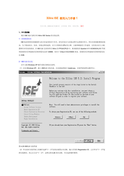
Xilinx ISE 使用入门手册1发布日期:2009-3-6 13:06:10文章来源:搜电浏览次数:58111、ISE的安装现以ISE 5.2i为例介绍Xilinx ISE Series的安装过程。
1)系统配置要求ISE 5.2i推荐的系统配置与设计时选用的芯片有关。
因为在综合与实现过程中运算量非常大,所以对系统配置要求很高。
为了提高综合、仿真、实现过程的速度,对于计算机的CPU的主频、主板和硬盘的工作速度,尤其是内存大小配置都有非常高的要求。
在ISE 5.2i支持的所有Xilinx的FPGA/CPLD中,要求最低的Spartan II和XC9500/XL/XV等系列需要的内存和虚拟内存推荐值均达到128MB,而对于Virtex-II XC2V8000来说,需要的内存和虚拟内存推荐值均高达3GB。
2)ISE 5.2i的安装以中文版Windows XP操作系统为例加以说明。
(1)启动Windows XP,插入ISE5.2i安装光盘,自动或选择执行Install.exe,安装界面如图4.25所示。
图4.25 ISE5.2i安装界面(2)单击此时安装界面上的操作选择“下一步”直到出现图示对话框,输入有效的Registration ID。
之后单击“下一步”选择安装路径;再之后点击“下一步”,会弹出图4.26的对话框,可以选择器件模型。
图4.26 器件模型选择对话框(3)点击“下一步”,如图4.27所示,可以选择器件种类。
图4.27 器件种类选择对话框通过以上步骤后,可根据具体情况来选择,继续“下一步”即可完成安装。
安装完成后,环境变量应作如下描述:若操作系统是Windows NT/2000/XP,选择开始->控制面板->系统->选项->系统->高级->环境变量,在环境变量中加入:变量名:Xilinx变量值:C:Xilinx(即安装路径)具体设置如图4.28所示。
图4.28 环境变量设置操作图3)安装第三方软件在PC上安装完ISE之后,还需要安装第三方仿真软件,如ModelSim等。
XILINX_时序约束使用指南中文

XILINX时序约束使用指南笔记第一章 时序约束介绍第二章 时序约束方法第三章 时序约束原则第四章 在XST中指定时序约束第五章 在Synplify中指定时序约束方法第六章 时序约束分析第一章 时序约束介绍 基本的时序约束包括:“PERIOD Constraints”“OFFSET Constraints”“FROM:TO(Multi‐Cycle)约束”第二章 时序约束方法1,简介:2,基本的约束方法根据覆盖的路径不同,时序要求变成一些不同的全局约束。
最普通的路径类型包括:1,输入路径2,同步元件到同步元件路径3,指定路径4,输出路径XILINX的时序约束与每一种全局约束类型都有关。
最有效的方法就是一开始就指定全局约束然后再加上指定路径的约束。
在很多案例中,只要全局约束就可满足需求。
FPGA器件执行工具都是由指定的时序要求驱动的。
如果时序约束过头的话,就会导致内存使用增加,工具运行时间增加。
更重要的是,过约束还会导致性能下降。
因此,推荐使用实际设计要求的约束值。
3,输入时序约束输入时序约束包括2种“系统同步输入”“源同步输入”输入时钟约束覆盖了输入数据的FPGA外部引脚到获取此数据的寄存器之间的路径。
输入时钟约束经常用”OFFSET IN”约束。
指定输入时钟要求的最好方法,取决于接口的类型(源/系统同步)和接口是SDR还是DDR。
OFFSET IN定义了数据和在FPGA引脚抓取此数据的时钟沿之间的关系。
在分析OFFSET IN 约束时,时序分析工具自动将影响时钟和数据延迟的因素考虑进去。
这些因素包括: 时钟的频率和相位转换时钟的不确定数据延迟调整除了自动调整,还可以在与接口时钟相关的”PERIOD”约束中另外增加时钟不确定。
关于增加”INPUT_JITTER”的更多信息,参见第三章的”PERIOD Constraints”。
“OFFSET IN”与单输入时钟有关,默认情况下,OFFSET IN约束覆盖了从输入pad到内部同步元件之间的所有路径。
xilinx ISE时序约束笔记-中文

时序约束的两个步骤:1.路径终点生产groups(顾名思义就是进行分组)2.指点不同groups之间的时序要求全局约束使用默认的路径终点groups——即所有的触发器、I/O pads等ISE时序约束笔记2——Global Timing Constraints问题思考单一的全局约束可以覆盖多延时路径如果箭头是待约束路径,那么什么是路径终点呢?所有的寄存器是否有一些共同点呢?问题解答什么是路径终点呢?——FLOP1,FLOP2,FLOP3,FLOP4,FLOP5。
所有的寄存器是否有一些共同点呢?——它们共享一个时钟信号,约束这个网络的时序可以同时覆盖约束这些相关寄存器间的延时路径。
周期约束周期约束覆盖由参考网络钟控的的同步单元之间的路径延时。
周期约束不覆盖的路径有:input pads到output pads之间的路径(纯组合逻辑路径),input pads到同步单元之间的路径,同步单元到output pads之间的路径。
周期约束特性周期约束使用最准确的时序信息,使其能够自动的计算:1.源寄存器和目的寄存器之间的时钟偏斜(Clock Skew)2.负沿钟控的同步单元3.不等同占空比的时钟4.时钟的输入抖动(jitter)假设:1.CLK信号占空比为50%2.周期约束为10ns3.由于FF2将在CLK的下降沿触发,两个触发器之间的路径实际上将被约束为10ns的50%即5ns时钟输入抖动(Clock Input Jitter)时钟输入抖动是源时钟的不确定性(clock uncertainty)之一时钟的不确定时间必须从以下路径扣除:——周期约束建立时间路径——OFFSET IN约束的建立时间路径时钟的不确定时间必须添加到以下路径中:——周期约束保持时间路径——OFFSET IN约束保持时间路径——OFFSET OUT约束路径Pad-to-Pad约束——不包含任何同步单元的纯组合逻辑电路——纯组合逻辑延时路径开始并结束于I/O pads,所以通常会被我们遗漏而未约束ISE时序约束笔记3——Global Timing Constraints问题思考哪些路径是由CLK1进行周期约束?哪些路径是由pad-to-pad进行约束?OFFSET约束OFFSET约束覆盖以下路径:——从input pads到同步单元(OFFSET IN)——从同步单元到output pads(OFFSET OUT)OFFSET约束特性OFFSET约束自动计算时钟分布延时1.提供最准确的时序信息2.大量增加输入信号到达同步单元的时间(时钟和数据路径并行)3.大量减少输出信号到达输出管脚的时间(时钟和数据路径先后)OFFSET约束也可以解释时钟输入抖动——使用抖动确定关联的周期约束时钟延时数据路径延时和时钟分布延时都需要在OFFSET计算中使用到——OFFSET IN = T_data_in –T_clk_in——OFFSET OUT = T_data_out + T_clk_outISE时序约束笔记4——Global Timing Constraints问题思考在这个电路中哪些路径是由OFFSET IN 和OFFSET OUT来约束的?问题解答:——OFFSET IN:PADA to FLOP and PADB to RAM——OFFSET OUT:LATCH to OUT1, LATCH to OUT2, and RAM to OU T1问题思考下面给出的系统框图里,你将给出什么样的约束值以使系统能够跑到100M Hz?——假设在下面的器件之间没有时钟偏斜问题解答:PERIOD = 10 ns , OFFSET IN (BEFORE) = 7 ns and OFFSET OUT (AF TER) = 8 ns小结1.性能期望和时序约束相关联2.周期约束覆盖同步单元之间的延时路径3.OFFSET约束覆盖从输入管脚到同步单元和从同步单元到输出管脚之间的延时路径ISE时序约束笔记5——Timing Groups and OFFSET C onstraints特定路径时序约束使用全局时序约束(PERIOD,OFFSET,PAD-TO-PDA)将约束整个设计仅仅使用全局约束通常会导致过约束——约束过紧——编译时间延长并且可能阻止实现时序目标——通过综合工具或者映射后时序报告重新审视性能评估特定路径约束能够覆盖全局时序约束在特定路径上的约束——这就允许设计者放宽特定路径的时序要求更多关于特定路径约束你的设计器件的内部面积将会从特定路径约束收益1.多周期路径Multi-cycle paths2.跨时钟域路径3.双向总线4.I/O时序特定路径约束应该由你的性能目标来界定,不能够不加限制的随意放置全局约束回顾使用全局PERIOD,OFFSET IN和OFFSET OUT约束将约束所有以下的路径这使得控制设计的总体性能更加容易特定路径约束实例一条特定路径约束对于路径本身的优化微乎其微这有助于你更好的控制设计性能,并带给执行工具更大的灵活性以达到你的性能和使用要求生成特定路径约束需要两个步骤:1.多个有共同时序要求的特定路径终点生成一个groups2.关联两个groups,指定它们的特定路径的时序要求生成终点路径的Groups特定路径时序约束在终点路径较好的分组后会更加高效——否则,约束一个大的工程将极其耗时耗力。
xilinx fpga中时钟输入管脚的约束

xilinx fpga中时钟输入管脚的约束在Xilinx FPGA中,时钟输入管脚的约束是非常重要的,它决定了时钟信号的稳定性和数据流的正确性。
以下是一些关于时钟输入管脚约束的相关参考内容。
1. 器件手册在Xilinx FPGA的器件手册中,通常会提供关于时钟输入管脚的详细信息。
这些信息包括时钟输入管脚的功能、电气特性、使用限制等。
器件手册还可能提供特殊的时钟输入约束,如最大工作频率、时钟插入延迟等。
2. 约束文件在设计FPGA时,通常会使用一个约束文件来指定设计中的时钟输入管脚的相关约束。
约束文件是一个文本文件,其中可以定义各种约束,如时钟频率、时钟插入延迟、时钟占空比等。
对于时钟输入管脚,约束文件通常会指定时钟源(如外部晶振或PLL)以及时钟的时钟域和时钟频率。
3. Vivado Design Suite User GuideVivado是Xilinx FPGA的设计工具套件,其用户指南提供了关于时钟输入管脚约束的详细信息。
用户指南中包含了各种约束的语法和用法,如时钟约束(CLOCK)以及时钟域(CLOCK_DOMAIN)。
用户指南还提供了一些示例和最佳实践,帮助设计师正确地约束时钟输入管脚。
4. 库元件和IP核的文档库元件和IP核是在FPGA设计中常用的组件。
对于这些组件,文档中通常会提供有关时钟输入管脚约束的信息。
例如,文档可能会包含有关时钟输入的建议,如时钟频率范围、时钟上升/下降时间要求等。
5. 官方论坛和社区Xilinx官方论坛和其他在线社区,如Xilinx FPGA设计社区,是一个寻求技术支持和问题解答的好地方。
这些论坛中的讨论和帖子通常包含关于时钟输入管脚约束的有用信息,如如何正确约束复杂时钟结构、如何解决时钟插入延迟等。
6. 应用笔记和技术文章Xilinx和其他第三方通常会发布一些应用笔记和技术文章,分享关于FPGA设计的有用信息。
这些文档中可能包含有关时钟输入管脚约束的实用技巧和教程,如如何避免时钟抖动、如何降低时钟插入延迟等。
- 1、下载文档前请自行甄别文档内容的完整性,平台不提供额外的编辑、内容补充、找答案等附加服务。
- 2、"仅部分预览"的文档,不可在线预览部分如存在完整性等问题,可反馈申请退款(可完整预览的文档不适用该条件!)。
- 3、如文档侵犯您的权益,请联系客服反馈,我们会尽快为您处理(人工客服工作时间:9:00-18:30)。
XILINX时序约束使用指南笔记第一章 时序约束介绍第二章 时序约束方法第三章 时序约束原则第四章 在XST中指定时序约束第五章 在Synplify中指定时序约束方法第六章 时序约束分析第一章 时序约束介绍 基本的时序约束包括:“PERIOD Constraints”“OFFSET Constraints”“FROM:TO(Multi‐Cycle)约束”第二章 时序约束方法1,简介:2,基本的约束方法根据覆盖的路径不同,时序要求变成一些不同的全局约束。
最普通的路径类型包括:1,输入路径2,同步元件到同步元件路径3,指定路径4,输出路径XILINX的时序约束与每一种全局约束类型都有关。
最有效的方法就是一开始就指定全局约束然后再加上指定路径的约束。
在很多案例中,只要全局约束就可满足需求。
FPGA器件执行工具都是由指定的时序要求驱动的。
如果时序约束过头的话,就会导致内存使用增加,工具运行时间增加。
更重要的是,过约束还会导致性能下降。
因此,推荐使用实际设计要求的约束值。
3,输入时序约束输入时序约束包括2种“系统同步输入”“源同步输入”输入时钟约束覆盖了输入数据的FPGA外部引脚到获取此数据的寄存器之间的路径。
输入时钟约束经常用”OFFSET IN”约束。
指定输入时钟要求的最好方法,取决于接口的类型(源/系统同步)和接口是SDR还是DDR。
OFFSET IN定义了数据和在FPGA引脚抓取此数据的时钟沿之间的关系。
在分析OFFSET IN 约束时,时序分析工具自动将影响时钟和数据延迟的因素考虑进去。
这些因素包括: 时钟的频率和相位转换时钟的不确定数据延迟调整除了自动调整,还可以在与接口时钟相关的”PERIOD”约束中另外增加时钟不确定。
关于增加”INPUT_JITTER”的更多信息,参见第三章的”PERIOD Constraints”。
“OFFSET IN”与单输入时钟有关,默认情况下,OFFSET IN约束覆盖了从输入pad到内部同步元件之间的所有路径。
用于抓取那些从pad输入的数据的同步元件由指定的OFFSET IN 时钟触发。
应用OFFSET IN约束被称为”global”方法。
这是指定输入时序的最有效的方法。
系统同步输入在体统同步接口中,发送和抓取数据共用一个系统时钟。
板上的布线延迟和时钟倾斜限制了接口的工作频率。
更低的频率也会导致系统同步输入接口典型的采用SDR应用。
系统同步SDR应用例子,见图2‐1。
系统同步SDR应用中,在时钟上升沿从源器件发送数据,下一个时钟上升沿在FPGA中抓取数据。
全局”OFFSET IN”约束是对一个系统同步接口指定输入时序的最有效的方法。
用这种方法,对每一个系统同步输入接口时钟都定义了一个”OFFSET IN”约束。
这种单个约束覆盖了所有被同步元件抓取到的输入数据位的路径,这些同步元件由指定输入时钟触发。
指定输入时序:1,定义接口相关的输入时钟的时钟”PERIOD”约束;2,定义接口的全局”OFFSET IN”约束;例子理想的系统同步SDR接口的时序图见图2‐2。
全局”OFFSET IN”约束是:OFFSET = IN <value> VALID <value> BEFORE clock;在”OFFSET IN”约束中,IN <value>决定了数据一开始有效的起始时间到抓取数据的时钟沿之间的时间。
在这个系统同步例子中,数据在抓取数据的时钟沿之前5ns有效。
VALID<value> 决定了数据有效时间。
在这个例子中,数据有效时间为5ns。
对这个例子,完整的”OFFSET IN”约束和相关的PERIOD约束如下:NET”SysClk”TNM_NET = “Sysclk”;TIMESPEC “TS_Sysclk” = PERIOD”SysClk” 5ns HIGH 50%;OFFSET = IN 5ns VALID 5ns BEFORE “SysClk”;源同步输入在源同步输入接口中,会重新产生时钟,重新生成的时钟和数据从源器件从相似的路径一起被传送出去。
这个时钟然后会被用来在FPGA中抓取数据。
电路板上的线路延时和板上的时钟倾斜都不会再限制接口的运行频率了。
更高的频率会导致源同步输入接口典型的被应用为双数据速率(DDR)的应用。
典型的源同步DDR应用见图2‐3。
在时钟上升沿和下降沿都会从源器件发送数据。
全局”OFFSET IN”约束是对源同步接口指定输入时序的最有效的方法。
在DDR接口,为每一个输入接口时钟的沿都会定义OFFSET IN约束。
这些约束覆盖了输入数据位的路径,这些数据由指定输入时钟沿的触发的寄存器来抓取。
要指定输入时序必须:1,为接口相关的输入时钟,定义时钟PERIOD约束;2,为接口上升沿定义全局OFFSET IN约束;3,为接口下降沿定义全局OFFSET IN约束;例源同步DDR接口的时序图见图2‐4,接口时钟是周期为5ns占空比为50%的时钟。
数据的每一位在半个周期内都有效。
对DDR全局OFFSET IN的约束如下:OFFSET = IN<value> VALID<value>BEFORE clock RISING;OFFSET = IN<value>VALID<value>BEFORE clock FALLING;在OFFSET IN约束中,OFFSET = IN<value>决定了从抓取时钟的时钟沿到数据开始有效的时间点之间的时间段。
以此源同步输入为例,上升沿传送的数据在时钟上升沿之前 1.25ns有效。
同样下降沿传送的数据在时钟下降沿之前 1.25ns有效。
在OFFSET IN约束中,VALID<value>决定了数据的有效时间。
在这个例子中,上升沿和下降沿的数据都保持了2.5ns。
此例中,OFFSET IN和与之相关的PERIOD约束如下:NET “SysCLK” TNM_NET = “SysCLK”;TIMESPEC “TS_SysClk” = PERIOD “SysClk” 5ns HIGH 50%;OFFSET = IN 1.25ns VALID 2.5ns BEFORE “SysClk” RISING;OFFSET = IN 1.25ns VALID 2.5ns BEFORE”SysClk”FALLING;4,寄存器到寄存器时序约束寄存器到寄存器或者“同步元件到同步元件”的路径约束覆盖了内部寄存器之间的同步数据路径。
PERIOD约束包含以下方面:1,定义了时钟域的时序要求;2,分析单时钟域里的路径;3,分析相关时钟域里的所有路径4,考虑不同时钟域中所有的频率,相位和时钟不确定性的不同点。
约束同步时钟域的应用和方法有以下几种,这些策略包括:1,“自动相关同步DCM/PLL时钟域”2,“手动相关同步时钟域”3,“异步时钟域”通过允许工具自动创造DLL/DCM/PLL和输出时钟之间的关系,和手动定义外部相关时钟之间关系,所有同步跨时钟域路径都有合适的约束覆盖,和合理的分析。
使用这些方法进行PERIOD约束就免去了额外的跨时钟域约束的必要。
自动相关同步DCM/PLL时钟域时钟电路最普通的形式是下面之一:1,输入时钟连接DLL/DCM/PLL;2,输出用来作为期间内部同步路径的时钟在这个例子中,推荐对连接到DLL/DCM/PLL的输入时钟做PERIOD约束。
通过对输入时钟进行PERIOD约束,XILINX工具自动:1,自动给每一个DLL/DCM/PLL的输出时钟派生出一个新的PERIOD约束;2,决定了输出时钟域之间的时钟关系,自动分析这些时钟域自己的任何路径例输入时钟驱动DCM的电路如图2‐5;本例的PERIOD约束语法如下:NET”ClockName” TNM_NET = “TNM_NET_Name”;TIMESPEC “TS_name” = PERIOD”TNM_NET_Name” PeriodValue HIGH HighValue%;在PERIOD约束中,”PeriodValue”定义了时钟周期的有效时间。
在本例中,DCM的输入时钟周期为5ns。
”HighValue”表示时钟波形为“HIGH”在一个时钟周期中所占的百分比。
本例的语法如下:NET “ClkIn” TNM_NET = “ClkIn”;TIMESPEC “TS_ClkIn” = PERIOD “ClkIn” 5 ns HIGH 50%;基于以上给出的输入时钟PERIOD约束,DCM自动:1,为DCM输出创造2个时钟约束2,在2个时钟域之间分析性能手动相关同步时钟域在某些情况下,同步时钟域之间关系不能由工具自动指定。
例如,当相关的时钟从两个独立的引脚进入FPGA时,碰到这种情况,XILINX推荐你用下面的步骤:1,为每一个输入时钟定义PERIOD约束;2,手动定义时钟之间关系;一旦你定义了手动关系,两个同步域之间的所有路径都会被自动分析。
分析将会把所有的,频率,相位和不确定信息考虑进去。
XILINX约束系统允许使用包含时钟频率和相位传送的PERIOD约束来定义时钟域之间complex manual relationship。
如果要使用PERIOD约束来定义时钟域之间的complex manual relationship,需要:1,为主时钟定义PERIOD约束;2,以第一个PERIOD约束作为参考,为相关时钟定义PERIOD约束;两个相关的时钟从2个独立的引脚进入FPGA,见图2‐61,clk1x是主时钟2,clk2x180是相关时钟本例的PERIOD约束语法如下:NET”PrimaryClock” TNM_NET = “TNM_Primary”;NET”RelatedClock” TNM_NET = “TNM_Related”;TIMESPEC “TS_primary” = PERIOD “TNM_Primary” PeriodValue HIGH HighValue%;TIMESPEC”TS_related” = PERIOD “TNM_Related” TS_Primary_relation PHASE value;在related PERIOD定义中,PERIOD值被定义为与主时钟的一个时间单元(period)关系。
这种关系以主时钟TIMESPEC的形式表达。
在本例中,CLK2X180的频率是CLK1X的2倍,这就导致PERIOD是其一半。
在related PERIOD定义中,相位值定义了源时钟和相关时钟在上升时钟沿的时间差异。
在本例中,因为CLK2X180时钟是180度相移,所以上升沿比主时钟的上升沿晚1.25ns。