PCB专业英语1
PCB工程部专业英语词汇
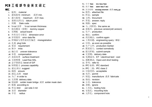
PCB 工程部专业英文词汇词汇1.板料: material2.最低限度: minimum 或者min.3.最大限度: maximum 或者max.4.基准点(零点) datum point5.周期Date code6.V-cut余厚V-cut remain thickness7.抢电铜皮(假铜)dummy copper8.实物板actual board9.外形及尺寸错误dimension error10.异常情形error data file11.焊锡面与零件面对位偏差misregistration12.孔塞plug hole13.要求requirement14.缺少miss15.偏公差uneven tolerance16.补偿compensation17.表面处理surface treatment18.无铅喷锡Lead free HAL19.金手指斜边bevel of G/F20.制程能力process capability21.建议,暗示suggest22.确保ensure23.满足,达到meet24.为了in order to25.交货期delivery date26.绿油桥solder mask bridge 或者solder mask dam27.根据according to28.单边3mil per side 3 mil29.直径diameter30.半径radius 31.小于3mil less than 3mil32.高于3mil more than 3 mil33.压合结构stacking structure 或者stack_up34.附件:attached file35.样品:sample36.文档:Document37.答复:answer; reply38.规格:spec39.与...同样的:the same as40.前版本:previous version(old version)41.生产:production42.确认:confirm43.再次确认:confirm again44.工程问题:engineering query(EQ)45.尽快:as soon as possible46.生产文件:production Gerber47.联系某人:contact somebody48.提交样板:submit sample49.交货期:delivery date50.电测成本:ET(electrical test)cost51.通断测试:Open and short testing52.参考:refer to53.IPC标准:IPC standard54.IPC二级:IPC class 255.可接受的:acceptable56.允许:permit57.制造:manufacture 或者fabricate58.修改:revision59.公差:tolerance60.忽略:ignore61.工具孔:tooling hole62.安装孔:mounting hole63.元件孔:component hole64.槽孔:slot hole65.邮票孔:snap off hole 或者stamp hole66.导通孔:via hole67.盲孔:blind via hole68.埋孔:buried via hole69.金属化孔:PTH(plated through hole)70.非金属化孔:NPTH( no plated through hole)71.孔位:hole location72.避免:avoid73.原设计:original design74.修改:modify75.按原设计:follow up original design76.附边:waste tab, waste area 或者breakaway tab77.铜条:copper strip78.拼板:panel drawing79.板厚:board thickness80.删除:remove(delete)81.削铜:shave the copper82.露铜:copper exposure 或者exposed copper83.光标点: fiducial mark84.不同:be different from(differ from)85.内弧:inside radius86.焊环:annular ring87.单板尺寸:single size88.拼板尺寸:panel size89.铣,锣:routing90.铣刀:router 或者Routing bit91.楔形掏槽V-cut 或者V scoring92.哑光:matt93.光亮的:glossy94.锡珠:solder ball(solder plugs)95.阻焊:solder mask(solder resist)96.阻焊开窗:solder mask opening 97.单面开窗:single side mask opening98.补油:touch up solder mask99.补线:track welds100.毛刺:burrs101.去毛刺:deburr102.镀层厚度:plating thickness103.清洁度:cleanliness104.离子污染:ionic contamination105.阻燃性等级:flammability retardant rating 106.黑化:black oxidation107.棕化:brown oxidation108.红化:red oxidation109.可焊性不良:poor solderability110.焊料:solder111.包装:packaging112.角标:corner mark113.特性阻抗:characteristic impedance 114.正像:positive115.负片:negative116.镜像:mirror117.线宽:line width 或者trace width118.线距:line spacing 或者trace spacing 119.做样:build sample120.按照:according to121.成品:finished122.做变更:make the change123.相类似:similar to124.规格:specification125.下移:shift down126.垂直地:vertically127.水平的:horizontally128.增大:increase129.缩小:decrease130.表面处理:Surface Finishing131.波峰焊:wave solder132.钻孔数据:drilling data133.标记:Logo134.Ul 标记:UL logo,或者Ul Marking135.蚀刻标记:etched marking136.周期:date code137.翘曲:bow and twist138.外层:outer layer 或者external layer139.内层:inner layer 或者internal layer140.顶层:top layer141.底层:bottom layer142.元件面:component side143.焊接面:solder side144.阻焊层:solder mask layer145.字符层:legend layer (silkscreen layer or over layer) 146.兰胶层:peelable SM layer147.贴片层:paste mask layer148.碳油层:carbon layer149.外形层:outline layer(profile layer)150.白油:white ink151.绿油:green ink152.喷锡:hot air leveling (HAL)153.电金,水金:flash gold154.插头镀金:plated gold edge-board contacts155.金手指:Gold-finger156.防氧化:Entek (OSP)157.沉金:Immersion gold (chem. Gold)158.沉锡:Immersion Tin(chem.Tin)159.沉银:Immersion Silver (chem. silver)160.单面板:single sided board161.双面板:double sided board162.多层板:multilayer board 163.刚性板:rigid board164.挠性板:flexible board165.刚挠板:flex-rigid board166.铣:CNC (mill , routing)167.冲:punching168.倒角:beveling169.斜面:chamfer170.倒圆角:fillet171.尺寸:dimension172.材料:material173.介电常数:Dielectric constant 174.菲林:film175.成像:Imaging176.板镀:Panel Plating177.图镀:Pattern Plating178.后清洗:Final Cleaning179.叠层:stacking structure (stack-up) 180.污染焊盘:contaminate pad181.分孔图:drill chart 或者drill map 182.度数:degree183.被…覆盖:be covered with184.负公差:minus tolerance185.标靶盘:target pad186.外形公差:routing tolerance 187.芯板:core188.半固化片Prepreg189.阻抗线:impedance trace190.评估estimate191.玻纤显露Fiber Exposure192.底铜base copper193.工作搞working Gerber194.原稿original art work195.放宽relax196.挖空blanking 或者cut-out197.一般性阻焊油墨general resist ink198.孔位错误mis hole location199.压合周期press cycle200.毛边serrated edges201.跳印skip printing202.气泡blistering203.隔离焊盘isolated pad204.泪滴tear drops205.箭头arrows206.加大Enlarge207.压合周期press cycle208.毛边serrated edges209.跳印,漏印skip printing210.宽度与厚度的比值width-to-thickness ratio 211.调整adjust212.铜箔基板copper claded laminates213.线路露铜copper exposure214.孔内异物dirty hole215.椭圆形elliptical set216.纤维突出fiber protrusion217.填充料filler218.互相连通interconnection219.改善方案implementation220.板料使用率material use factor221.回路,网络network222.缺口nick223.氧化oxidation224.剥离(剥落) peeling off225.补线不良poor touch-up226.品质等级quality classification227.对位孔registration228.拒收rejectable 229.树脂含量resin content230.排列电阻resistor network231.锣刀(铣刀)routing bit232.孔内沾文字S/L on hole233.孔内绿漆S/M on hole234.线路沾锡solder on trace235.金手指沾锡solder on G/F236.废框scrap237.封孔处理sealing238.间距不足spacing non-enough 239.靶位孔target hole240.测试线路test circuit241.热应力试验thermal stress242.厚度分布thickness distribution 243.薄基板,内层板thin core244.线路缺口及针孔track nick & pin hole 245.裁切线trim line246.真平整true leveling247.真正位置的孔true position248.万用型universal249.气化室vaporizer250.仓库warehouse251.契尖角wedge angle252.线细width reduce253.良率yield254.渗铜,渗入,灯芯效应wicking255.允收acceptable256.试样点coupon location257.经核准的,被认可的approved258.超越胜过,超过其他exceed259.牛皮纸kraft paper260.孔壁破铜Hole void261.孔位破出Hole breakoutPCB生产—经典流程—英文培训教程A. 开料( Cut Lamination)a-1 裁板( Sheets Cutting)a-2 原物料发料(Panel)(Shear material to Size)B. 钻孔(Drilling)b-1 内钻(Inner Layer Drilling )b-2 一次孔(Outer Layer Drilling )b-3 二次孔(2nd Drilling)b-4 雷射钻孔(Laser Drilling )(Laser Ablation )b-5 盲(埋)孔钻孔(Blind & Buried Hole Drilling)C. 干膜制程( Photo Process(D/F))c-1 前处理(Pretreatment)c-2 压膜(Dry Film Lamination)c-3 曝光(Exposure)c-4 显影(Developing)c-5 蚀铜(Etching)c-6 去膜(Stripping)c-7 初检( Touch-up)c-8 化学前处理,化学研磨( Chemical Milling )c-9 选择性浸金压膜(Selective Gold Dry Film Lamination) c-10 显影(Developing )c-11 去膜(Stripping )Developing , Etching & Stripping ( DES )D. 压合Laminationd-1 黑化(Black Oxide Treatment)d-2 微蚀(Microetching)d-3 铆钉组合(eyelet )d-4 叠板(Lay up)d-5 压合(Lamination)d-6 后处理(Post Treatment)d-7 黑氧化( Black Oxide Removal ) d-8 铣靶(spot face)d-9 去溢胶(resin flush removal)E. 减铜(Copper Reduction)e-1 薄化铜(Copper Reduction)F. 电镀(Horizontal Electrolytic Plating)f-1 水平电镀(Horizontal Electro-Plating) (Panel Plating) f-2 锡铅电镀( Tin-Lead Plating ) (Pattern Plating)f-3 低于1 mil ( Less than 1 mil Thickness )f-4 高于1 mil ( More than 1 mil Thickness)f-5 砂带研磨(Belt Sanding)f-6 剥锡铅( Tin-Lead Stripping)f-7 微切片( Microsection)G. 塞孔(Plug Hole)g-1 印刷( Ink Print )g-2 预烤(Precure)g-3 表面刷磨(Scrub)g-4 后烘烤(Postcure)H. 防焊(绿漆/绿油): (Solder Mask)h-1 C面印刷(Printing Top Side)h-2 S面印刷(Printing Bottom Side)h-3 静电喷涂(Spray Coating)h-4 前处理(Pretreatment)h-5 预烤(Precure)h-6 曝光(Exposure)h-7 显影(Develop)h-8 后烘烤(Postcure)h-9 UV烘烤(UV Cure)h-10 文字印刷( Printing of Legend )h-11 喷砂( Pumice)(Wet Blasting)h-12 印可剥离防焊(Peelable Solder Mask)I . 镀金Gold platingi-1 金手指镀镍金( Gold Finger )i-2 电镀软金(Soft Ni/Au Plating)i-3 浸镍金( Immersion Ni/Au) (Electroless Ni/Au)J. 喷锡(Hot Air Solder Leveling)j-1 水平喷锡(Horizontal Hot Air Solder Leveling)j-2 垂直喷锡( Vertical Hot Air Solder Leveling)j-3 超级焊锡(Super Solder )j-4. 印焊锡突点(Solder Bump)K. 成型(Profile)(Form)k-1 捞型(N/C Routing ) (Milling)k-2 模具冲(Punch)k-3 板面清洗烘烤(Cleaning & Backing)k-4 V型槽( V-Cut)(V-Scoring)k-5 金手指斜边( Beveling of G/F)L. 开短路测试(Electrical Testing) (Continuity & Insulation Testing) l-1 AOI 光学检查( AOI Inspection)l-2 VRS 目检(Verified & Repaired)l-3 泛用型治具测试(Universal Tester)l-4 专用治具测试(Dedicated Tester)l-5 飞针测试(Flying Probe)M. 终检( Final Visual Inspection)m-1 压板翘( Warpage Remove)m-2 X-OUT 印刷(X-Out Marking)m-3 包装及出货(Packing & shipping)m-4 目检( Visual Inspection)m-5 清洗及烘烤( Final Clean & Baking)m-6 护铜剂(ENTEK Cu-106A)(OSP)m-7 离子残余量测试(Ionic Contamination Test )(Cleanliness Test)m-8 冷热冲击试验(Thermal cycling Testing)m-9 焊锡性试验( Solderability Testing )N. 雷射钻孔(Laser Ablation)N-1 雷射钻Tooling孔(Laser ablation Tooling Hole)N-2 雷射曝光对位孔(Laser Ablation Registration Hole)N-3 雷射Mask制作(Laser Mask)N-4 雷射钻孔(Laser Ablation) N-5 AOI 检查及VRS ( AOI Inspection & Verified & Repaired) N-6 Blaser AOI (after Desmear and Microetching)N-7 除胶渣(Desmear)N-8 微蚀(Microetching )。
pcb线路板专业英语(中英)
不定形的改變
amount
總量
amyl nitrite
硝基戊烷
analyzer
分析儀
anneal
回火
annular ring
環狀墊圈;孔環
anode slime (sludge)
陽極泥
anodizing
陽極處理
AOI ( automatic optical inspection )
自動光學檢測
applicable documents
補償
competitive performance
競爭力績效
complex salt
錯化物
complexor
錯化物
component hole
零件孔
component sid
conformance
密貼性
consumer products
消費性產品
contact resistance
1
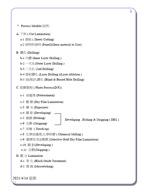
* Process Module 說明 :
A. 下料 ( Cut Lamination) a-1 裁板 ( Sheets Cutting) a-2 原物料發料 (Panel)(Shear material to Size)
B. 鑽孔 (Drilling) b-1 內鑽 (Inner Layer Drilling ) b-2 一次孔(Outer Layer Drilling ) b-3 二次孔 (2nd Drilling) b-4 雷射鑽孔 (Laser Drilling )(Laser Ablation ) b-5 盲(埋)孔鑽孔 (Blind & Buried Hole Drilling)
K. 成型 (Profile)(Form)
PCB基本英语.
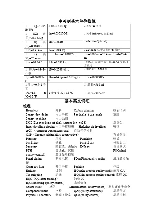
流程Board cut 开料Carbon printing 碳油印刷Inner dry film 内层干膜Peelable blue mask 蓝胶Inner etching 内层蚀刻ENIG(Electroless nickel immersion gold) 沉镍金Inner dry film stripping 内层干膜退膜HAL(hot air leveling) 喷锡AOI(Automatic Optical Inspection)自动光学检测OSP(Organic solderability preservative)有机保焊Pressing 压板Punching 啤板Drilling 钻孔Profiling 外形加工Desmear 除胶渣,去钻污 E-Test 电性测试PTH 镀通孔,沉铜FQC(final quality control) 最终品质控制Panel plating 整板电镀FQA(Final quality audit) 最终品质保证Outer dry film 外层干膜Packing 包装Etching 蚀刻IPQA(In-process quality audit) 流程QA Tin stripping 退锡IPQC(In-process quality control) 流程QC EQC(QC after etching)蚀检QCIQC(Incoming quality control) 来料检查Solder mask 感阻MRB(material review board) 材料评审委员会Component mark 字符QA(Quality assurance) 品质保证Physical Laboratory 物理实验室QC(Quality control) 品质控制Chemistry Laboratory 化学实验室Document control center 文件控制中心2nd Drilling 二钻Routing 锣板,铣板Brown oxidation 棕化Waste water treatment 污水处理V-cut V坑WIP(work in process)半成品Store/stock 仓库 F.G(Finished goods) 成品概述Printed Circuit Board 印制电路板Flexible Printed Circuit, FPC 软板Double-Side Printed Board 双面板IPC(The Institute for Interconnecting and Packing Electronic Circuits)电子电路互连与封装协会CPAR(Corrective & Preventive Action Request)要求纠正预防措施Flammability Rate燃性等级Characteristic impedance 特性阻抗BUM(Build-up multilayer)积层多层板Date Code周期代码CCL(Copper-clad laminate)覆铜板Ionic contamination 离子性污染Acceptance Quality Level (AQL)允收水平HDI(High density interconnecting)高密度互连板Base Material基材Radius 半径Capacity 生产能力Diameter 直径Capability 工艺能力PPM(Parts Per Million) 百万分之几CAM(computer-aided manufacturing) 计算机辅助制造Underwriters Laboratories Inc. 美国保险商实验所CAD (computer-aided design) 计算机辅助设计Statistical Process Control 统计过程控制Specification 规格,规范Via 导通孔Dimension 尺寸Buried /blind via 埋/盲孔Tolerance 公差Tooling hole 定位孔Oven 焗炉Output/throughput 产量湿流程PTH(plated through hole)镀通孔(俗称沉铜)Acid cleaning 酸性除油PP(Panel Plating) 板电Acid dip 酸洗Pattern plating 图电Pre-dip 预浸Line width 线宽Alkaline cleaning 碱性除油Spacing 线隙Flux 松香Deburring 去毛刺(沉铜前磨板)Hot air leveling 喷锡Carbon treatment 碳处理Skip plating 跳镀,漏镀Track/conductor 导线Undercut 侧蚀Aspect ratio深径比Water rinsing水洗Etch Factor 蚀刻因子Transportation 行车Back Light Test背光测试Rack挂架Pink ring粉红圈Maintenance 保养干流程Hole location孔位Annular ring 孔环Image Transfer图象转移Component Side(C/S) 元件面Artwork 底片Solder Side(S/S) 焊接面Mylar 胶片Matte Solder Mask 哑绿油Silkscreen/legend/Component Mark文字Hole breakout 破孔Fiducial mark 基点,对光点Scrubbing 磨板Expose 曝光Developing 显影内层制作Core material 内层芯板Thermal pad 散热PAD Pre-preg PP片Resin content 树脂含量Kraft Paper牛皮纸Brown oxidation 棕化Lay up 排版Black Oxidation 黑化Registration 对位Base material 板材Delamination 分层其它Wicking灯芯效应Hole size 孔径(尺寸) Yield良品率Touch Up修理Warp and Twist 板曲度Solvent Test 溶剂测试Peel off 剥离Company Logo 公司标识Tape Test 胶纸试验UL Mark UL 标记Cosmetic 外观Function 功能Tin/Lead Ratio 锡/铅比例Reliability Tests 可靠性试验Hole Wall Roughness 孔壁粗糙度Base Copper Thickness 底铜厚度PCB专业英语(PCB SPECIAL ENGLISH)1.PCB=Printed Circuit Board 电路板2.CAM=Computer aided manufacture 计算机辅助3.Pad 焊盘4.Annular ring 焊环5.AOI=automatic optical inspection 自动光学检测6.Charge of free 免费7.WIP=work in process 在线板8.DCC=document control center 文控中心9.Legend 字符10.CS=Component Side =Top Side (顶层)元件面11.SS=Solder Side =Bottom Side (底层)焊锡面12.Gold Plated 电金,镀金13.Nickel Plated 电镍,镀镍14.Immersion Gold 沉金=沉镍金15.Carbon Ink Print 印碳油16.Microsection Report 切片报告,横切面报告17.X-out=Cross-out 打"X"报告18.Panel (客户称)拼板,(生产线称)工作板19.Marking 标记,UL 标记20.Date code 生产周期21.Unit 单元,单位22.Profile 外形,轮廓<outline>23.Profile By Routing 锣(铣)外形24.Wet Film 湿菲林,湿绿油,湿膜25.Slot 槽,方坑26.Base Material=Base Laminate 基材,板料27.V-out =V-score V形槽28.Finished 成品29.Marketing 市场部30.Gerber File GERBER文件31.UL LOGO UL标记32.E-Test=Electric Open/Short Test 电子测试33.PO=Purchase Order 订单34.Tolerance 公差35.Rigid,Flexible Board 刚性,软性板36.Board cut 开料37.Board baking 焗板38.Drill 钻孔39.PTH=Plated Through Hole 镀通孔,沉铜40.Panel plating 板面电镀,全板电镀41.Photo Image 图象,线路图形42.Pattern plating 线路电镀43.Etching 蚀板,蚀刻44.SM=Solder Mask 防焊,阻焊,绿油45.SR=Solder Resist 防焊,阻焊,绿油46.Gold finger 金手指47.Silkscreen 丝印字符48.HAL=HASL=Hot air(Solder)leveling 热风整平喷锡49.Routing 锣板,铣板50.Punching 冲板,啤板51.FOC=final quality checking 终检,最后检查52.FOA=final quality audit 最后稽查(抽查)53.Shippment 出货54.Flux 松香55.Au金,Cu铜,Ni镍,Pb铅,Tn锡,Tin-lead锡铅合金56.Lead free 无铅57.COC=compliance of certificate 材料证明书58.Microsection=cross section 微切片,横切片59.Chamical gold 沉镍金60.Mould=punch die 模具,啤模61.MI=manufacture instruction 制作批示62.QA=quality assurance 品质保证63.CAD=computer aided design 计算机辅助设计64.Drill bit size钻咀直径<diameter>65.Bow and twist 板弯和板曲66.Hit 击打,孔数67.Bonding 邦定,点焊68.Test coupon 测试模块(科邦)69.Thieving copper 抢电流铜皮70.Rail-web71.Break-up tab 工艺边72.Break away tab 工艺边73.GND=ground 地线,大铜皮74.Hole edge 孔边,孔内75.Stamp hole 邮票孔76.Template 天坯,型板,钻孔样板(首板)77.Dry film 干菲林,干膜78.LPI=liquid photo image 液态感光=湿绿油79.Multilayer 多层板80.SMD=surface mouted device 贴片,表面贴装器件81.SMT=surface mouted technology 表面贴装技术82.Peelable mask=blue gel 蓝胶83.Tooling hole 工艺孔,管位,定位孔,工具孔84.Fiducial mask 测光点,光学对位点,对光点,电眼85.Copper foil 铜箔86.Dimension 尺寸87.Nagative负的,positive正的88.Flash gold 闪镀金,镀薄金89.Engineering department 工程部90.Delivery date 交货期91.Bevelling 斜边92.Spacing=gap 间隙,气隙,线隙PCB的各层定义及描述为了方便与印制板厂家的技术沟通,提高对PCB的技术认知一致度,特在此将我司常用PCB的有关板层特性做简单说明,请爱好者参考此说明进行设计和制造。
PCB专业英译术语
PCB专业英译术语PCB(Printed Circuit Board,印刷电路板)是现代电子产品中最常用的一种重要的电路载体,其设计、生产和维修需要大量的技术术语支持。
本文将重点介绍PCB专业英译术语。
一、PCB基础术语1. PCB(Printed Circuit Board):印刷电路板2. SMT(Surface Mount Technology):表面贴装技术3. Through-hole Technology:通孔技术4. PTH(Plated Through Hole):贯穿电解孔5. FR4:一种常用的印刷电路板基材材料,即玻璃纤维材料,通常由环氧树脂和玻璃纤维材料构成6. Pad:焊盘7. Trace:线路8. Via:垂直插孔9. Gerber file:Gerber文件格式,一种电路板设计文件格式10. BOM(Bill of Materials):物料清单11. NC(Numerical Control):数控12. DFM(Design for Manufacturability):可制造性设计二、PCB制造过程相关术语1. CAM(Computer Aided Manufacturing):计算机辅助制造2. Etch:蚀刻3. Silkscreen:丝网印刷4. Solder mask:焊盘油墨5. Plating:电镀6. HASL(Hot Air Solder Leveling):热风焊盘处理7. OSP(Organic Solderability Preservatives):有机可焊保护剂8. Gold Fingers:金手指,指电子产品中可进行插拔操作的特殊金属触点9. DIP(Dual In-line Package):双列直插封装10. SOP(Small Outline Package):小封装11. QFN(Quad Flat Package):四角平封12. BGA(Ball Grid Array):球网阵列13. PCBA(Printed Circuit Board Assembly):印刷电路板装配三、PCB测试和维修相关术语1. AOI(Automated Optical Inspection):自动光学检测2. X-ray Inspection:X光检测3. ICT(In-Circuit Test):在线测试4. FCT(Functional Circuit Test):功能测试5. Test point:测试点6. Defect:缺陷7. Repair:修复8. Rework:返工9. Troubleshooting:故障排除四、PCB设计相关术语1. EDA(Electronic Design Automation):电子设计自动化2. Netlist:网表3. DRC(Design Rule Check):设计规则检查4. DFM(Design for Manufacturing):可制造性设计5. Gerber data:Gerber数据6. Simulation:仿真7. Library:元件库8. Footprint:封装9. Copper pour:铜质填充10. Via tenting:垂直插孔塞堵11. Blind vias:盲孔12. Buried vias:穿过孔五、总结本文介绍了PCB专业英译术语中的基础术语、PCB制造过程相关术语、PCB测试和维修相关术语以及PCB设计相关术语。
PCB&FPC专业英语
PCB专用词语A aA.O.I(Automatic Optical Inspection) 自动光学检查Acceptable quality level (AQL) 可接受质量水平Accuracy 精确度Activating 活化Active carbon treatment 活性碳处理After Pressed Thickness 压板后之厚度Alignment 校直,结盟Annular ring 锡圈Anti-Static Bag 静电胶袋Apparatus 设备,仪器Area 面积Artwork 菲林Artwork Drawing 菲林图形Artwork Film 原装菲林Artwork Modification 菲林修改Artwork No. 菲林编号Assembly 组装,装配Axis 轴B bBackplane 背板Back-up 垫板Baking 烘板Ball Grid Array (BGA) 球栅阵列Bare board 裸板Base Copper 底铜Base material 基材Bevelling 斜边Black Oxide 黑氧化Blind via hole 盲孔Blistering 起泡/水泡Board Cutting 开料Board Thickness 板厚Bottom side 底层Breakaway tab 打断点Brushing 磨刷Build-up 积层Bullet pad 子弹盘Buried hole 埋孔C cC/M(Component Marking) 元件字符Carbon ink 碳油Carrier 带板Ceramic substrate 陶瓷Certificate of Compliance 合格证书Chamfer 倒角Chemical cleaning 化学清洗Chemical corrosion 化学腐蚀Chip Scale Package (CSP) 晶片比例包装Circuit 线路Clearance 间距/间隙Color 颜色Component Side(C/S) 元件面Composite layers 复合层Computer Aided Design (CAD) 电脑辅助设计Computer Aided Manufacturing (CAM) 电脑辅助制作Computer Numerial Control (CNC) 数控Conductor 导体Conductor width/space 导体线宽/线隙Contact 接点Copper area 铜面积Copper clad 铜箔Copper foil 铜箔Copper plating 电镀铜Corner 角线Corner mark 板角记号Corner REG.Hole 角位对位孔Cracking 裂缝Creasing 皱折Criteria 规格,标准Crossection area 切面Cu/Sn Plating 镀铜锡Current efficiency 电流效率Customer 客户Customer Drilling File 客户钻孔资料Customer P/N 客户产品编号D dD/F Registration Hole 干菲林对位孔D/F(Dry Film) 干膜Date Code 日期代号Datum hole 基准参考孔Daughter board 子板Deburring 去毛刺Defect 缺陷Definition 定义Delamination 分层Delay 耽搁Delivery 交货Densitomefer 透光度计Density 密度Department 部门Description 说明Design origin 设计原点Desmear 去钻污,除胶Dessicant 防潮珠Developer 显影液,显影机Diamond 钻石Diazo film 重氮片Dielectric breakdown 介电击穿Dielectric constant 介电常数Dielectric Thickness 介电层厚度Dielectric V oltage Test 绝缘测试Dimension 尺寸Dimensional stability 尺寸稳定性Direct/indirect 直接/间接Distribution 发放Document type 文件种类Documentation Control 文件控制Double sided board 双面板Drill bit 钻咀Drilling 钻孔Drilling Roughness 钻孔粗糙度Dry Film 干菲林Dry Film-Pattern 干膜线路Dynamic 动态E eECN(Engineering Change Notification) 工程更改通知Effective date 有效期Electrical Test Fixture 电测试针床Electro migration 漏电Electroconductive paste 导电胶Electroless 无电沉Electroless copper 无电沉铜Electroless Ni 无电沉镍Electroless Gold/Au 无电沉金Engineering drawing 工程图纸Entek 有机涂覆Epoxy glass substrate 环氧玻璃基板Epoxy resin 环氧基树脂Etch 蚀刻Etchback 凹蚀Etching 蚀刻E-Test Marking 电测试标记E-Test(Electrical Test) 电测试Exposure 曝光External layer 外层F fFiducial mark 基准点Filling 填充Film Fabrication 菲林制作Final QC 最终检查Finish Overall Board Thickness 成品总板厚度Fixture 夹具Flammability 可燃性Flash Gold 薄金Flexible 易曲的,能变形的Flux 助焊剂G gGeneral information 一般资料Ghost image 重影Glass transition temperature 玻璃化湿度Gold Finger(G/F) 金手指Golden board 金板Grid 网格Ground plane 地线层H hHAL(Hot Air Leveling) 热风整平Hand Rout 手锣Hardness 硬度Heat Sealed 热密封Heat Shrink-warp 热收缩Holding time 停留时间Hole 孔Hole breakout 破环Hole density 孔的密度Hole Diameter 孔径Hole location 孔位Hole Location Chart 孔位座标表Hole Position Tolerance 孔位误差Hole size 孔尺寸Hot Air Leveling(HAL) 热风整平Humidity 湿度IIdentification 标识,指标Image 影像Imaging transfer 图形转移Impedance 阻抗Impedance Test 阻抗测试Inner copper foil 内层铜箔Inspection 检验Insulation resistance Test 绝缘测试Inter Plane Separation 内层分离Interleave Paper 隔纸Internal layer 内层Internal stress 内应力Ionic cleanliness 离子清洁度Isolation 孤立Isolation Resistance 绝缘电阻Item 项目K kKEY board 按键盘Key slot 槽孔Kraft paper 牛皮纸L lLaminate 板材Laminate Thickness 材料厚度Lamination void 层间空洞Landless hole 破孔Laser plotter 激光绘图机Laser plotting 激光绘图Laser via hole 激光穿孔Layup 层压配本Lay-up Instruction 压板指示Legend 字符Legend Width 字符宽度Length 长度Lifted Lands 残铜Line Width 线宽Liquid 液体Logic diagram 逻辑图形Logo 唛头,标记Lot size 批卡Mesh 目数M mMark 标记Master drawing 菲林图形Material Thickness 材料厚度Material Type 材料类型Max. X-out 坏板上限Max.Board Thickness After Plating 电镀后总板厚度之上限Measling 白斑Mech Drawing No. 图纸编号Mechanical cleaning 机械清洗Metal 金属Method 方法MI(Manufacturing Instruction) 生产制作指示Microstrip 微条线Min Conductor Copper Thickness 最小线路铜厚Min Hole Wall Copper Thickness 最小孔壁铜厚Min. Gold Plating Thickness 最小金厚Min. Nickel Thickness 最小镍厚Min. Tin-Lead Thickness (After HAL) (喷锡后)最小锡厚Min.Annular Ring 最小环宽Min.Spacing between Line to Line 线与线之间的最小距离Min.Spacing between Line to Pad 线与焊盘之间的最小距离Min.Spacing between Pad to Pad 焊盘与焊盘之间的最小距离Minimum 最小Mirroring 镜像Missing 缺少Model No. 产品名称Molded 模塑Mother board 主板Moulding 模房Mounting hole 安装孔Multilayer 多层板Multi-layer Laminate 多层板材料N nNegative 反面的Net list 网络表Nick 缺口No. of holes 孔数No.of Array/Panel 每个拼板套板数No.of Panel per Stack 每叠板数No.of Panel/Sheet 每张大料拼板数No.of Pcs Per Bag 每包数量No.of Unit/Array 每套单元数Normal value标准值O oOblong 椭圆形的Offset 偏移Open/short 开路/短路Optimization(design) 最佳化(设计)Organic Solerability Peservatives(OSP) 有机保护剂Originator 原作者Outer copper foil 外层铜箔Outline 外形P pPacking 包装Packing 包装Pad 焊盘Panel Area 拼板面积Panel Plated Crack 板镀缺口Panel plating 整板电镀Panel Size 拼板尺寸Panel Size After Outerlayer Cutting 外层切板后拼板尺寸Panel Utilization 拼板利用率Pass rate 通过率Passivation 钝化Pattern 线路Pattern Inspection 线路检查Pattern plating 图形电镀PCB(Printed Circuit Board) 印制线路板Peck drilling 啄钻Peel strength 剥离强度Peelable 可剥性Peelable 剥离强度Peelable Mask 可脱油Peeling 剥离Permanent 永久性PH value PH值Photo plotting 图形输出Photo via hole 菲林过孔Photographers 照片靶标Photoplotler 光绘机Physical 物理的Pin hole 销定孔Pink ring 粉红环Pinning hole 钻孔管位Pitch 间距Placement 放置Plated Though Hole(PTH) 沉铜Plating 电镀Plating Crack 电镀裂缝Plating line 电镀线Plating rack 电镀架Plating V oid 电镀针孔Plug Hole 塞孔Polymer 聚合体Porosity 孔隙率Positive 绝对的Power plane 电源层Prepreg 半固化片Primary side 首面Print 印刷Probe point 针床测点Process 工序Process flow 工序流程Product Planning Dept. 生产计划部Production 生产板Profile 外形Profiling 外形加工Profiling Process 外形加工Project No. 产品编号PTH Thermal Seress Test PTH热冲击测试PTH(Plating Through Hole) 沉铜Pull away 拉离Punch 啤模Punching 冲切Punching Mould Drawing 啤模图形Q qQA Audit 品质审计QA(Quanlity Assurance) 品质部Quad Palt Pack (QFP) 四边扁平林整器件Quantity 数量R rRaw Material Utilization 原材料利用率Recall 回收Rectifier 整流器Register mark 对位点Registration 重合点Remark 备注Resin 树脂Resin Recession 流胶Resist 抗蚀剂Resolution 分辨率Rigid 精密的Roller coating 涂覆Roughening 粗化Round pad 圆盘Routing 外形加工,铣板S sS/M Material 绿油物料S/M(Solder Mask) 阻焊Sales 销售Sample 样板Sampling inspection 抽样检验Scaling factor 缩放比例因素Scope 范围Scoring 刻槽Scratch 划痕Secondary side 第二面Section Code 组别代号Section Code Change 组别代号更改Segment 部分,片段Separated 分离Sequence 顺序Sets 套Sheet Size 大料尺寸Shematic diagram 原理图Shiny 有光泽的,发光的Silk screen 丝印Silver film 银盐片Single/double 单层/双面Slot 槽,坑Solder Mask 阻焊Solder mask on bare copper (smobc) 裸铜覆盖阻焊膜Solder side 焊接面Solder Side C/M 阻焊面字符Solder Side Cir. 焊接面线路Solder Side Circuit 焊接面Solder Side S/M 焊接面阻焊Solderability 可焊性Solvent Test 可溶性测试Spacing 线距Special requirement 特殊要求Specification 详细说明,规范Spindle 主轴Split 裂片Square pad 方块Standard 标准值Static 静态Stencial 网版Step drilling 分布钻Step scale 光梯尺Store 货仓Supplier 供应商Supported hole 支撑点Surface 表面Surface mount technology 表面组装技术Swimming 滑移T tTack 堆起Tape Programming 铬带制作Tape Test 胶带测试Target Hole 目标孔Teardrop 泪珠Template 天平Tenting 封孔Test 测试Test coupon 图样Test Parameter 测试参数Test Pattern 测试孔Testing V oltage 电压Thermal shock 热冲击Thermal stress 热应力Thickness 厚度Tin Content 锡含量Tin/Lead Stripping 退铅锡Tin-lead plating 电镀铅锡Tolerance 公差Top side 板面Touch up 修理(执漏)Training 训练Transmission 传输线Transmittance 传送Trim line 修剪U uUltrasonic cleaning 超声波清洗Undercut 侧蚀Unit Arrangement 单元排版Unit Layout Per Panel 单元拼板图Uv-blocking 阻挡紫外线V vVacunm Pack 真空包装Vacuum lamination 真空压制V-Cut V- 坑View From…观察方向由…Visual & Warpage 可视性和翘曲度Visual inspection 目检V oltage 电压W wW/F(Wet Film) 湿膜Warp & Twist 翘曲和弯曲Wet Film 湿模Width 宽度Wiring 线路。
PCB工厂专业英语

標簽 層 電橋器 條形物 腳 漏 洩漏 漏電流 長度 線 線性的 組 電源線 列示 低的
米 儀表 儀器 磁鐵 磁石 磁性的 手冊 手工的 手動 邊緣 安全膠布 印章 最大值 測量 測量值 測試 外觀尺寸 迎合 滿足 符合 最小值 毫米 必須
材料明細表
BTO
Build To Order
接單生產
CAD/CAM Computer Aided Design/Manufactur CAR
Calibration Corrective Action Response
儀器校驗 (儀校) 改善對策報告
CCR
Customer Complain Requirement
客戶抱怨/要求
Charge Charge
索取費用
CND
Cannot Duplicate
無法複製,異常現象消失
CR
Critical
嚴重(CR>MA>MI)
CS
Customer Service
客戶服務
CTO
Configure To Order
接單組裝
Debit Note Debit Note
(會計) 帳目通知
測試工程
Total Productive Maintenance
全面性生產維護
Total Quality Management
全面品質管理
TUV
德國萊茵技術監護顧問公司 (安規單位)
Underwriters Laboratories
美國保險協會實驗室 (安規單位)
Vender Quality Approval
PCB专业术语翻译(英语)
PCB专业术语(英语)PCB printed circuit board 印刷电路板,指空的线路板PCBA printed circuit board assembly 印刷电路板组件,指完成元件焊接的线路板组件PW A Printed Wire Assembly,Aperture list Editor:光圈表编辑器。
Aperture list windows:光圈表窗口。
Annular ring:焊环。
Array:拼版或陈列。
Acid trip:蚀刻死角。
Assemby:安装。
Bare Bxnel:光板,未进行插件工序的PCB板。
Bad Badsize:工作台,工作台有效尺寸。
Blind Buried via:盲孔,埋孔。
Chamfer:倒角。
Circuit:线路。
Circuit layer:线路层。
Clamshell tester:双面测试机。
Coordinates Area:坐标区域。
Copy-protect key:软件狗。
Coutour:轮廓。
Draw:一种圆形的光圈,但只是用于创建线路,不用于创建焊盘。
Drill Rack:铅头表。
Drill Rack Editor:铅头表编辑器。
Drill Rack window:铅头表窗口。
D Code:Gerber格式中用不着于表达光圈的代码。
Double-sided Biard:双面板。
End of Block character(EOB):块结束符。
Extract Netlist:提取网络。
Firdacial:对位标记。
Flash:焊盘,来源于早期矢量光绘机,在矢量光绘机中,焊盘是光通过光圈“闪出”(Flash)而形成的。
Gerber Data:从PCB CAD系统到PCB生产过程中最常用的数据格式。
Grid :栅格。
Graphical Editor:图形编辑器。
Incremental Data:增量数据。
Land:接地层。
Layer list window:层列表窗口。
PCB专业英语和层定义
PCB专业英语(PCB SPECIAL ENGLISH)1.PCB=Printed Circuit Board 电路板2.CAM=Computer aided manufacture 计算机辅助3.Pad 焊盘4.Annular ring 焊环5.AOI=automatic optical inspection 自动光学检测6.Charge of free 免费7.WIP=work in process 在线板8.DCC=document control center 文控中心9.Legend 字符10.CS=Component Side =Top Side (顶层)元件面11.SS=Solder Side =Bottom Side (底层)焊锡面12.Gold Plated 电金,镀金13.Nickel Plated 电镍,镀镍14.Immersion Gold 沉金=沉镍金15.Carbon Ink Print 印碳油16.Microsection Report 切片报告,横切面报告17.X-out=Cross-out 打“X”报告18.Panel (客户称)拼板,(生产线称)工作板19.Marking 标记,UL 标记20.Date code 生产周期21.Unit 单元,单位22.Profile 外形,轮廓<outline>23.Profile By Routing 锣(铣)外形24.Wet Film 湿菲林,湿绿油,湿膜25.Slot 槽,方坑26.Base Material=Base Laminate 基材,板料27.V-out =V-score V形槽28.Finished 成品29.Marketing 市场部30.Gerber File GERBER文件31.UL LOGO UL标记32.E-Test=Electric Open/Short Test 电子测试33.PO=Purchase Order 订单34.Tolerance 公差35.Rigid,Flexible Board 刚性,软性板36.Board cut 开料37.Board baking 焗板38.Drill 钻孔39.PTH=Plated Through Hole 镀通孔,沉铜40.Panel plating 板面电镀,全板电镀41.Photo Image 图象,线路图形42.Pattern plating 线路电镀43.Etching 蚀板,蚀刻44.SM=Solder Mask 防焊,阻焊,绿油45.SR=Solder Resist 防焊,阻焊,绿油46.Gold finger 金手指47.Silkscreen 丝印字符48.HAL=HASL=Hot air(Solder)leveling 热风整平喷锡49.Routing 锣板,铣板50.Punching 冲板,啤板51.FOC=final quality checking 终检,最后检查52.FOA=final quality audit 最后稽查(抽查)53.Shippment 出货54.Flux 松香55.Au金,Cu铜,Ni镍,Pb铅,Tn锡,Tin-lead锡铅合金56.Lead free 无铅57.COC=compliance of certificate 材料证明书58.Microsection=cross section 微切片,横切片59.Chamical gold 沉镍金60.Mould=punch die 模具,啤模61.MI=manufacture instruction 制作批示62.QA=quality assurance 品质保证63.CAD=computer aided design 计算机辅助设计64.Drill bit size钻咀直径<diameter>65.Bow and twist 板弯和板曲66.Hit 击打,孔数67.Bonding 邦定,点焊68.Test coupon 测试模块(科邦)69.Thieving copper 抢电流铜皮70.Rail-web71.Break-up tab 工艺边72.Break away tab 工艺边73.GND=ground 地线,大铜皮74.Hole edge 孔边,孔内75.Stamp hole 邮票孔76.Template 天坯,型板,钻孔样板(首板)77.Dry film 干菲林,干膜78.LPI=liquid photo image 液态感光=湿绿油79.Multilayer 多层板80.SMD=surface mouted device 贴片,表面贴装器件81.SMT=surface mouted technology 表面贴装技术82.Peelable mask=blue gel 蓝胶83.Tooling hole 工艺孔,管位,定位孔,工具孔84.Fiducial mask 测光点,光学对位点,对光点,电眼85.Copper foil 铜箔86.Dimension 尺寸87.Nagative负的,positive正的88.Flash gold 闪镀金,镀薄金89.Engineering department 工程部90.Delivery date 交货期91.Bevelling 斜边92.Spacing=gap 间隙,气隙,线隙PCB的各层定义及描述为了方便与印制板厂家的技术沟通,提高对PCB的技术认知一致度,特在此将我司常用PCB的有关板层特性做简单说明,请爱好者参考此说明进行设计和制造。
- 1、下载文档前请自行甄别文档内容的完整性,平台不提供额外的编辑、内容补充、找答案等附加服务。
- 2、"仅部分预览"的文档,不可在线预览部分如存在完整性等问题,可反馈申请退款(可完整预览的文档不适用该条件!)。
- 3、如文档侵犯您的权益,请联系客服反馈,我们会尽快为您处理(人工客服工作时间:9:00-18:30)。
Printed Circuit Board ENGLISH Training
PCB专业英语培训教材
本培训针旨在介绍PCB基本的专业英语,并对PCB专业英语分以下几个部分:
1.P CB 分类
2.P CB 材料
3.P CB 生产流程
4.水处理
5.P CB 检验
6.主要设备
7.工程设计
8.元器件组装
1.PCB Sort (PCB 分类):
Single sided board(单面板) Double sided Board(双面板) Multilayer Board(多层板) Rigid board(刚性板) flexible board(挠性板) flex-rigid board(刚挠结合板) metal base PCB(金属基板)
Blind board(盲孔板) buried board(埋孔板) bare board (裸板)
Quick turn prototype(样板)
2.PCB Material(PCB 材料):
Copper clad laminate(CCL)(覆铜板) PREPREG(半固化片) Epoxy resin(环氧树脂) Copper foil(铜箔)
PTFE (Polytetralluoetylene) Teflon(聚四氟乙烯) dielectric constant(介电常数)Flexible copper clad(挠性覆铜板) silver film(银盐片) diazo film(重氮片) Solder mask(阻焊) Dry film(干膜) legend ink(字符油墨) peelable solder mask(可
剥离阻焊) flux(助焊剂) additive(添加剂)
3.PCB Process(PCB 生产流程) :
Wet process(湿法流程) Dry process(干法流程)
FOR MULTILAYER MANUFACTURE PROCESS(多层线路板生产流程):
Laminate cut(覆铜板) scrubbing(擦板) Image transfer(图形转移) internal layer (内层) Exposure(曝光) Developing(显影) ETCHING(蚀刻) black / brown oxygen (黑/棕化) lay up(叠层) Laminating(层压) Drilling(钻孔) scrubbing(擦
板) Plated through hole(孔金属化) PTH panel plating(板面电镀) pattern plating (plated resist) (图形电镀) Etching(蚀刻)Inspection(检验) Printing solder mask(阻焊印刷) Exposure(曝光) Developing(显影) Hot Cured(热固化)Hot Air Leveling(热风整平)IMMERSION GOLD(沉金) Printing legend ink (silkscreen printing)(字符印刷)Hot Cured(热固化) Routing(铣外形)punch(冲孔) Bare board testing(裸板测试) Final Inspection(终检) Packing(包装) Delivery(发货)
4.Water treatment(水处理)
DI (dialysis ion) water(去离子水) Waste water treatment(污水处理) humidity (湿度)temperature(温度)
5.PCB Inspection(PCB 检验):
Inspection standard(检验标准) defect open(开路) short(短路) measling(白斑) fibre exposure(漏基材) hole breakout(破孔) flatness(平面度) peel strength(剥离强度) thermal shock(热冲击) thermal stress(热应力) Reworking (返工) manufacture panel(制造拼板) light integrator(光积分仪) step scale (光尺) undercut factor(侧蚀系数) micro etching(微蚀) over etching (过蚀) swimming(滑移)
6.Major equipments(主要设备):
Laser plotter(激光光绘机) CNC drilling machine(数控钻床) CNC routing machine (数控铣床) Scrubber(擦板机) Auto through hole plating line(自动沉铜线)panel plating line(板面电镀线) pattern plating line (plated resist) (图形电镀线) dry film laminator(贴膜机) Exposure(曝光机) developing line(显影线) Etching line(蚀刻线) Auto registration punch(冲孔机) Multilayer press system(多层板层压系统) Black oxidation line(黑化线) Automatic optical instrument AOI(自动光学检测仪) Flying Probe test FPT(飞针检测仪) Hot air leveling(热风整平机) Impedance control test system(阻抗控制检测仪)
7.Engineering Design(工程设计):
lay out(布线) CAD (computer aided design) (计算机辅助设计) CAM (computer aided manufacture) (计算机辅助制造) EDA (Electronic design automatic) (电子设计自动化) origin(原点) mirroring(镜相) scaling factor(比例系数) network (网络) conductor track(导线) PAD(焊盘) width(宽度) gap spacing(间隙)aperture(光圈) round(圆形) oblong(长圆形) square(正方形) rectangle (长方形) tear pad(泪滴焊盘) isolation pad(隔离焊盘) thermal pad(热焊盘)
mounting hole(安装孔) via(过孔) Plating through hole PTH(金属化孔) NPTH (非金属化孔) tooling hole(定位孔) Fiducial (基准点、反光点) layer to layer spacing(层间距) layer Building up drawing(层叠图) external layer(外层) internal layer(内层) power layer(电源层) ground layer(接地层) signal line(信号线) target(标靶) slot(槽孔) tab connector (golden finger) (金手指) Impedance control PCB(阻抗控制) Golden board(黄金板) MI (manufacture information) (制造说明) NOPE ( no process engineering ) (重订单) photo plotting(laser plotting)(激光光绘) positive(正片) negative (负片)
8.Component Assembly(元器件组装):
SMT (Surface mount technology) (表面贴装技术)
Bonding(邦定) DIP(dual inline package) (双列直插封装) QFP(quad flat package) (四面扁平封装) BGA(ball grid array ) (球栅封装)
SMD (Surface mount devices) (表面贴装设备) Placement machine(贴装机)REFOLW SOLDERING(回流焊) WAVE SOLDERING(波峰焊)。