FM2113(单节锂电池保护IC)
锂电池保护IC
UPA1870BGR 封装:TSSOP-8 品牌:NEC 备注:配套MOS管
FS8205A 封装:TSSOP-8 品牌:富晶 备注:配套MOS管
SM8205ACTC 封装:SOT-23-6 品牌:茂达 备注:配套MOS管
R5402N163KD-TR-F 封装:SOT-23-6 品牌:RICOH 备注:单节
R5460N207AF 封装:SOT-23-6 品牌:RICOH 备注:双节
R5460N207AA 封装:SOT-23-6 品牌:RICOH 备注:双节
R5460N208AA 封装:SOT-23-6 品牌:RICOH 备注:双节
SM8205AOC 封装:TSSOP-8 品牌:茂达 备注:配套MOS管
AO8810 封装:TSSOP-8 品牌:AOS 备注:配套MOS管
AO8820 封装:TSSOP-8 品牌:AOS 备注:配套MOS管
AO8822 封装:TSSOP-8 品牌:AOS 备注:配套MOS管
S-8254AAJFT-TB-G 封装:TSSOP-17 品牌:SEIKO 备注:三-四节
S-8254AANFT-TB-G 封装:TSSOP-18 品牌:SEIKO 备注:三-四节
S-8254AAKFT-TB-G 封装:TSSOP-19 品牌:SEIKO 备注:三-四节
R5400N101FA-TR-F 封装:SOT-23-5 品牌:RICOH 备注:单节
R5402N110KD-TR-F 封装:SOT-23-6 品牌:RICOH 备注:单节
R5402N149KD-TR-F 封装:SOT-23-6 品牌:RICOH 备注:单节
移动电源锂电保护IC宏康HY2113规格书
HY2113规格书1节锂离子/锂聚合物电池保护IC .目录概述1. (5)特点2. (5)应用3. (5)方框图4. (6)订购信息5. (6)产品目录6. (7)电气参数选择6.1. (7)6.2. (8)延迟时间代码-延迟时间参数选择6.3. (9)特性代码-其它功能选择封装、脚位及标记信息7. (9)绝对最大额定值8. (11).电气特性9. (12)电气参数(延迟时间除外)9.1. (12)9.2. (13)延迟时间参数电池保护IC应用电路示例10. (14)工作说明11. (15)正常工作状态11.1. (15)11.2. (15)过充电状态11.3. (15)过放电状态11.4. (16)放电过流状态(放电过流检测功能和负载短路检测功能)11.5. (16)充电过流状态11.6. (17)向0V电池充电功能(允许)11.7. (17)向0V电池充电功能(禁止)特性(典型数据)12. (18)封装信息13. (21)DFN-6L 封装13.1. (21)13.2. (22)SOT-23-6封装14. (23)修订记录.注意:1、本说明书中的内容,随着产品的改进,有可能不经过预告而更改。
请客户及时到本公司网站下载更新。
2、本规格书中的图形、应用电路等,因第三方工业所有权引发的问题,本公司不承担其责任。
3、本产品在单独应用的情况下,本公司保证它的性能、典型应用和功能符合说明书中的条件。
当使用在客户的产品或设备中,以上条件我们不作保证,建议客户做充分的评估和测试。
4、请注意输入电压、输出电压、负载电流的使用条件,使IC内的功耗不超过封装的容许功耗。
对于客户在超出说明书中规定额定值使用产品,即使是瞬间的使用,由此所造成的损失,本公司不承担任何责任。
5、本产品虽内置防静电保护电路,但请不要施加超过保护电路性能的过大静电。
6、本规格书中的产品,未经书面许可,不可使用在要求高可靠性的电路中。
例如健康医疗器械、防灾器械、车辆器械、车载器械及航空器械等对人体产生影响的器械或装置,不得作为其部件使用。
单片 IC MM1433 锂离子电池充电控制用(1~2节电池用) 说明书

MITSUMI ()HE jin hui 135******** 锂离子电池充电控制用(1~2节电池用)本IC 是锂离子电池充电控制用IC ,只用本IC 就可进行稳流、稳压充电,同时是一种内置预充电、过充电定时器、电池温度检测功能等保护电路的单片充电IC 。
本IC 在以前充电用的MM1332、MM1333的基础上,增加了上述功能。
(1) 充电电压精度(Ta = 0°C ~ +50°C) ±30mV/节(2) 消耗电流5mA 典型值(3) 预充电功能(4) 再次充电功能(5) 充电超时定时器(6) 电池温度检测功能(7) 适配器(初级)异常检测功能(8) LED 驱动器(R 、G 端子)(9) 备有1节或2节电池TSOP-24A锂离子电池充电控制用MITSUMI锂离子电池充电控制用(1~2节电池用)TSOP-24A注:上图是典型的应用实例参考,对因使用这些电路所造成的损害或对第三者工业所有权的侵犯,本公司不承担任何责任。
3509633055MITSUMI锂离子电池充电控制用(1~2节电池用)1注1:电流限制值1、2及满充电检测规定使用电流检测电阻上的电压降的对应值。
注2:如本IC损坏,控制失效时,不能保证安全。
请用本IC以外的装置来加以保护。
注3:温度检测用B常数3435(石冢电子公司产品10KC15-1608)的设定值。
注4:OSC部分的电容器请使用温度特性好的元件。
电容器的特性差异会造成定时器的误差。
注5:对过放电电池,用1mA电流充电14秒,在此期间不转换到预充电状态时,本IC将判定该电池异常。
OSC CR设定参考资料(1) OSC CR-振荡周期T一览表实例(2)各定时器的时间1基本功能•稳压/稳流控制充电•满充电检测2保护功能• AC适配器/电池异常时的保护•利用电池温度监视功能,工作异常时进行保护•利用时间限制功能,工作异常时进行保护3显示功能•显示正常充电结束状态的绿色LED连续点亮•显示正常充电工作状态的红色LED连续点亮•显示检测到异常时充电禁止的红色LED闪亮•限时用内部定时器的工作状态检查4强制停止功能•通过RESET端子、CHGSW端子控制停止充电5恢复充电功能•通过满充电检测后的电池电压降的检测进行重新充电•通过AC适配器断开后的再连接进行重新充电•通过电池断开后的再连接进行重新充电•通过解除强制停止工作进行重新充电说明1.充电动作1.1充电开始•充电开始时,在以下场合充电处于禁止状态。
单节锂电池保护解决方案(3)

单节锂电池保护解决方案(3)CSS-3---单节电池保护解决方案引言:前面两节分别介绍了PCM的几种方案,本节聚焦于PCM 的性能评估以及可能遇到的问题优化。
1. 功率(MOSFET)的性能要求离子电池容量从早期的600mAh、1000mAh到现在已经达到6000mAh、10000mAh。
为了实现更快的充电速度和更短的充电时间,通常采用增加(电流)和大电流充电的快充技术。
大电流充电对电池组中的功率MOSFET提出了更高的技术要求。
此外在生产线和使用过程中,对大容量(锂离子电池)有一些特定的技术要求。
所有这些因素都对大容量锂离子电池PCM中功率MOSFET的充放电管理提出了严格的技术设计挑战。
为了实现功率MOSFET的低导通电阻RDSon,有必要提高MOSFET单元密度。
其他技术也用于降低电阻,例如厚金属键合线和薄晶片。
N沟道功率MOSFET可以以减小的形状因数实现较低的导通电阻RDSon。
功率MOSFET封装通常使用引线,为了进一步降低导通电阻,在PCM中通过使用新的(芯片)级CSP封装技术完全消除了封装线电阻。
同时芯片级CSP的封装技术具有更好的导热性,从而降低功率MOSFET的温升,这有助于提高其可靠性。
使用CSP封装技术的功率MOSFET在没有外部塑料外壳和其他材料保护的情况下,在PCM生产过程中会受到各种热应力和(机械)应力的影响,例如(PCB)板的焊接过程,这可能会导致模具开裂的高风险。
因此应使用各种技术,例如在功率MOSFET芯片表面涂覆新材料,以确保其抵抗机械应力和热应力的能力,并提高可靠性。
短路能力大容量锂离子电池在应用中,特别是在极端条件下,如输出负载短路,会有非常大的电流通过电池。
当IC(检测)到输出过流时,它将延迟一段时间以进行保护动作。
在延迟时间期间,MOSFET的工作电流非常大,这要求MOSFET对大电流应力具有鲁棒性,因此所有锂离子电池都需要进行短路测试。
理论上芯片尺寸越大,对短路电流的鲁棒性越强。
士兰微电子 内置MOSFET的单节锂电池保护芯片SC8821 说明书

SC8821
过充电状态→负载放电→正常状态
杭州士兰微电子股份有限公司
版本号:1.2 2009.05.05 共10页 第5页
过放电状态→充电器正常充电→正常状态
SC8821
过放电状态→充电器异常充电→正常状态
杭州士兰微电子股份有限公司
充电器时, VDD电压大于VOCU,且延迟时间超过TOC,则电池电压进入到过充电状态,VBAT端电流为0,停止对电池充电。
杭州士兰电子股份有限公司
版本号:1.2 2009.05.05 共10页 第3页
SC8821
释放过充电状态 进入过充电状态后,要解除过充电状态,返回正常状态,有两种方法。 • 如果电池自我放电,并且VDD<VOCR ,返回到正常状态。 • 在移去充电器,连接负载后,如果VOCR<VDD<VOCU且VCSI>VOI1,返回到正常状态。
则返回到正常状态。
异常充电检测 当电池在正常状态时,VBAT+与VBAT-之间接充电器,若VCSI<VCH ,延迟时间超过TOC,
则VBAT-端电流为0,停止对电池充电。
过电流/短路电流检测 在正常状态下,VBAT+与VBAT-之间接负载,当放电电流太大时,检测到CSI端电压大于
VOIX(VIO1或VIO2),并且延迟时间大于TOIX (TIO1或TIO2),则代表过电流(短路)状态,CSI端 通过内部电阻RCSIS拉到VSS,VBAT-端电流为0,VBAT-端电压由于负载的原因而拉到VDD。
SC8821
内置MOSFET的单节锂电池保护芯片
描述
SC8821是内置MOSFET的单节锂电池保护芯片,为避 免锂电池因过充电、过放电、电流过大导致电池寿命缩短或 电池被损坏而设计的。SC8821具有高精确度的电压检测与 时间延迟功能。
PW3133A超简单的单节锂电池保护电路
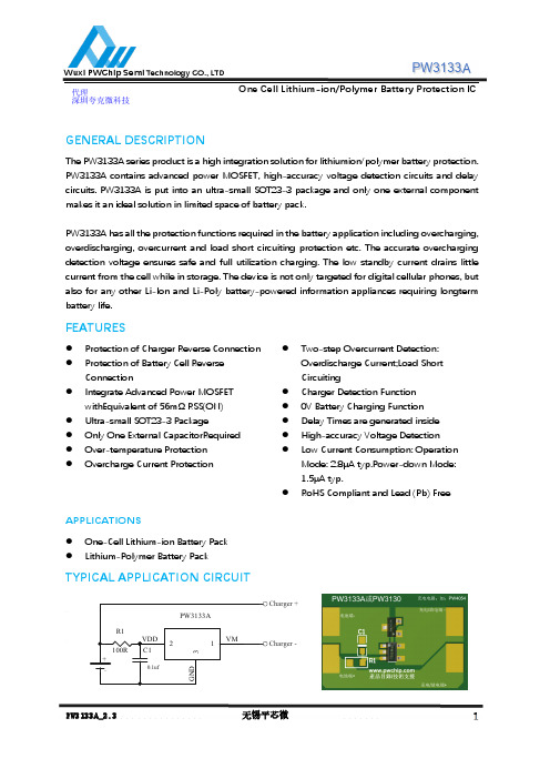
PW3133AOne Cell Lithium-ion/Polymer Battery Protection ICGENERAL DESCRIPTIONThe PW3133A series product is a high integration solution for lithiumion/polymer battery protection. PW3133A contains advanced power MOSFET, high-accuracy voltage detection circuits and delay circuits. PW3133A is put into an ultra-small SOT23-3 package and only one external component makes it an ideal solution in limited space of battery pack.PW3133A has all the protection functions required in the battery application including overcharging, overdischarging, overcurrent and load short circuiting protection etc. The accurate overcharging detection voltage ensures safe and full utilization charging. The low standby current drains little current from the cell while in storage. The device is not only targeted for digital cellular phones, but also for any other Li-Ion and Li-Poly battery-powered information appliances requiring longterm battery life.FEATURES● Protection of Charger Reverse Connection ● Protection of Battery Cell ReverseConnection● Integrate Advanced Power MOSFETwithEquivalent of 56mΩ RSS(ON) ● Ultra-small SOT23-3 Package● Only One External CapacitorRequired ● Over-temperature Protection ● Overcharge Current Protection● Two-step Overcurrent Detection :Overdischarge Current;Load Short Circuiting● Charger Detection Function ● 0V Battery Charging Function ● Delay Times are generated inside ● High-accuracy Voltage Detection ● Low Current Consumption: OperationMode: 2.8μA typ.Power-down Mode: 1.5μA typ.● RoHS Compliant and Lead (Pb) FreeAPPLICATIONS● One-Cell Lithium-ion Battery Pack ● Lithium-Polymer Battery PackTYPICAL APPLICATION CIRCUIT代理深圳夸克微科技Wuxi PWChip Semi Technology CO., LTDELECTRICAL CHARACTERISTICSTypicals and limits appearing in normal type apply for TA = 25oC, unless otherwise specifiedNote: The parameter is guaranteed by design .ParameterSymbol Test Condition Min Typ Max UnitDetection VoltageOvercharge Detection Voltage V CU4.254.30 4.35VOvercharge Release Voltage V CL 4.054.10 4.15VOverdischarge Detection VoltageV DL 2.3 2.4 2.5VOverdischarge Release Voltage V DR2.93.03.1VDetection CurrentOverdischarge Current1Detection *I IOV1V DD =3.6V3.5A Load Short-Circuiting Detection*I SHORT V DD =3.6V20ACurrent ConsumptionCurrent Consumption in Normal OperationI OPE V DD =3.6V VM =0V 2.86μA Current Consumption in power DownI PDNV DD =2.0VVM pin floating1.53μAVM Internal Resistance Internal Resistance between VM and V DD*R VMD VDD=2.0V VM pin floating 300k ΩInternal Resistance between VM and GND*R VMSV DD =3.6V VM=1.0V20k ΩFET on ResistanceEquivalent FET on Resistance *R SS(ON)V DD =3.6V I VM =1.0A56m ΩOver Temperature Protection Over T emperature Protection*T SHD+150oCOver T emperature Recovery Degree *T SHD-110Detection Delay TimeOvercharge Voltage Detection Delay Timet CU 80130200mS Overdischarge Voltage Detection Delay Timet DL 204060mS Overdischarge Current Detection Delay Time*t IOV V DD =3.6V 4816mS Load Short-Circuiting Detection Delay Time*t SHORTV DD =3.6V80180300uSFunctional Block DiagramOPERATIONThe PW3133A monitors the voltage and current of a battery and protects it from being damaged due to overcharge voltage, overdischarge voltage, overdischarge current, and short circuit conditions by disconnecting the battery from the load or charger. These functions are required in order to operate the battery cell within specified limits.The device requires only one external capacitor. The MOSFET is integrated and its RSS(ON) is as low as 56mΩ typical.Normal operating modeIf no exception condition is detected, charging and discharging can be carried out freely. This condition is called the normal operating mode.Overcharge ConditionWhen the battery voltage becomes higher than the overcharge detection voltage (VCU) during charging under normal condition and the state continues for the overcharge detection delay time (tCU) or longer, the PW3133A turns the charging control FET off to stop charging. This condition is called the overcharge condition. The overcharge condition is released in the following two cases:1, When the battery voltage drops below the overcharge release voltage (VCL), the PW3133A turns the charging control FET on and returns to the normal condition.2, When a load is connected and discharging starts, the PW3133A turns the charging control FET on and returns to the normal condition. The release mechanism is as follows: the discharging current flows through an internal parasitic diode of the charging FET immediately after a load is connected and discharging starts, and the VM pin voltage increases about 0.7 V (forward voltage of the diode) from the GND pin voltage momentarily. The PW3133A detects this voltage and releases the overcharge condition. Consequently, in the case that the battery voltage is equal to or lower than the overcharge detection voltage (VCU), the PW3133A returns to the normal condition immediately, but in the case the battery voltage is higher than the overcharge detection voltage (VCU),the chip does not return to the normal condition until the battery voltage drops below the overcharge detection voltage (VCU) even if the load is connected. In addition, if the VM pin voltage is equal to or lower than the overcurrent 1 detection voltage when a load is connected and discharging starts, the chip does not return to the normal condition.Remark If the battery is charged to a voltage higher than the overcharge detection voltage (VCU) and the battery voltage does not drops below the overcharge detection voltage (VCU) even when a heavy load, which causes an overcurrent, is connected, the overcurrent 1 and overcurrent 2 do not work until the battery voltage drops below the overcharge detection voltage (VCU). Since an actual battery has, however, an internal impedance of several dozens of mΩ, and the battery voltage drops immediately after a heavy load which causes an overcurrent is connected, the overcurrent 1 and overcurrent 2 work. Detection of load shortcircuiting works regardless of the battery voltage.Overdischarge ConditionWhen the battery voltage drops below the overdischarge detection voltage (VDL) during discharging under normal condition and it continues for the overdischarge detection delay time (tDL) or longer, the PW3133A turns the discharging control FET off and stops discharging. This condition is called overdischarge condition. After the discharging control FET is turned off, the VM pin is pulled up by the RVMD resistor between VM and VDD in PW3133A.Meanwhile when VM is bigger than 1.5V (typ.) (the load short-circuiting detection voltage), the current of the chip is reduced to the power-down current (IPDN). This condition is called power-down condition. The VM and VDD pins are shorted by the RVMD resistor in the IC under the overdischarge and power-down conditions. The power-down condition is released when a charger is connected and the potential difference between VM and VDD becomes 1.3 V (typ.) or higher (load shortcircuiting detection voltage). At this time, the FET is still off. When the battery voltage becomes the overdischarge detection voltage (VDL) or higher (see note), the PW3133A turns the FET on and changes to the normal condition from the overdischarge condition.Remark If the VM pin voltage is no less than the charger detection voltage (VCHA), when the battery under overdischarge condition is connected to a charger, the overdischarge condition is released (the discharging control FET is turned on) as usual, provided that the battery voltage reaches the overdischarge release voltage (VDU) or higher.When the discharging current becomes equal to or higher than a specified value (the VM pin voltage is equal to or higher than the overcurrent detection voltage) during discharging under normal condition and the state continues for the overcurrent detection delay time or longer, the PW3133A turns off the discharging control FET to stop discharging. This condition is called overcurrent condition. (The overcurrent includes overcurrent, or load short-circuiting.)The VM and GND pins are shorted internally by the RVMS resistor under the overcurrent condition. When a load is connected, the VM pin voltage equals the VDD voltage due to the load. The overcurrent condition returns to the normal condition when the load is released and the impedance between the B+ and Bpins becomes higher than the automatic recoverable impedance. When the load is removed, the VM pin goes back to the GND potential since the VM pin is shorted the GND pin with the RVMS resistor. Detecting that the VM pin potential is lower than the overcurrent detection voltage (VIOV1), the IC returns to the normal condition.Abnormal Charge Current DetectionIf the VM pin voltage drops below the charger detection voltage (VCHA) during charging under the normal condition and it continues for the overcharge detection delay time (tCU) or longer, the PW3133A turns the charging control FET off and stops charging. This action is called abnormal charge current detection. Abnormal charge current detection works when the discharging control FET is on and the VM pin voltage drops below the charger detection voltage (VCHA). When an abnormal charge current flows into a battery in the overdischarge condition, the PW3133A consequently turns the charging control FET off and stops charging after the battery voltage becomes the overdischarge detection voltage and the overcharge detection delay time (tCU) elapses.Abnormal charge current detection is released when the voltage difference between VM pin and GND pin becomes lower than the charger detection voltage (VCHA) by separating the charger. Since the 0 V battery charging function has higher priority than the abnormal charge current detection function, abnormal charge current may not be detected by the product with the 0 V battery charging function while the battery voltage is low.Load Short-circuiting conditionIf voltage of VM pin is equal or below short circuiting protection voltage (VSHORT), the PW3133A will stop discharging and battery is disconnected from load. The maximum delay time to switch current off is tSHORT. This status is released when voltage of VM pin is higher than short protection voltage (VSHORT), such as when disconnecting the load.Delay CircuitsThe detection delay time for overdischarge current 2 and load short-circuiting starts when overdischarge current 1 is detected. As soon as overdischarge current 2 or load short-circuiting is detected over detection delay time for overdischarge current 2 or load short- circuiting, the PW3133A stops discharging. When battery voltage falls below overdischarge detection voltage due to overdischarge current, the PW3133A stop discharging by overdischarge current detection. In thisPW3133Acase the recovery of battery voltage is so slow that if battery voltage after overdischarge voltage detection delay time is still lower than overdischarge detection voltage, the PW3133A shifts to power-down.Overcurrent delay time0V Battery Charging Function (1) (2) (3)This function enables the charging of a connected battery whose voltage is 0 V by self-discharge. When a charger having 0 V battery start charging charger voltage (V0CHA) or higher is connected between B+ and B- pins, the charging control FET gate is fixed to VDD potential. When the voltage between the gate and the source of the charging control FET becomes equal to or higher than the turn-on voltage by the charger voltage, the charging control FET is turned on to start charging. At this time, the discharging control FET is off and the charging current flows through the internal parasitic diode in the discharging control FET. If the battery voltage becomes equal to or higher than the overdischarge release voltage (VDU), the normal condition returns.Note(1) Some battery providers do not recommend charging of completely discharged batteries. Please refer to battery providers before the selection of 0 V battery charging function.(2) The 0V battery charging function has higher priority than the abnormal charge current detection function. Consequently, a product with the 0 V battery charging function charges a battery and abnormal charge current cannot be detected during the battery voltage is low (at most 1.8 V or lower).(3) When a battery is connected to the IC for the first time, the IC may not enter the normal condition in which discharging is possible. In this case, set the VM pin voltage equal to the GND voltage (short the VM and GND pins or connect a charger) to enter the normal condition.TIMING CHART1. Overcharge and overdischarge detectionOvercharge and Overdischarge Voltage Detection2. Overdischarge current detectionOverdischarge Current DetectionRemark: (1) Normal condition (2) Overcharge voltage condition (3) Overdischarge voltage condition (4)Overcurrent conditionVV CU -VV DL +V VDLONONCHARGEV DD Vov1VSS VVM Charger Load V CUV CU -V HCV DL +V DHV DLONDISCHARGE OFF V DD V V ov2V ov1V SSCharger Load(1)(4)(1)(1)(1)(4)(4)Charger Detection4. Abnormal Charger DetectionAbnormal Charger DetectionRemark: (1) Normal condition (2) Overcharge voltage condition (3) Overdischarge voltage condition (4) Overcurrent conditionVV CU -V V DL +V V DL ON Charger Load V DDV SSV VMVVCU -VV DL +VV DL ON ONCHARGE VDD V SS VVM Charger LoadTYPICAL APPLICATIONAs shown in Figure 6, the bold line is the high density current path which must be kept asshort as possible. For thermal management, ensure that these trace widths are adequate. C1 is a decoupling capacitor which should be placed as close as possible to PW3133A.PW3133A in a Typical Battery Protection CircuitPrecautions• Pay attention to the operating conditions for input/output voltage and load current so that the power loss in PW3133A does not exceed the power dissipation of the package.• Do not apply an electrostatic discharge to this PW3133A that exceeds the performance ratings of the built-in electrostatic protection circuit.PW3133A 11 PW3133A_2.3 PACKAGE DESCRIPTION SOT23-3无锡平芯微。
AMS电源芯片产品介绍
AMS3132,3A 低压差稳压器
输入电压范围:1.5-7V 输出电压固定或可调 最低输出0.6V每100mV一个步进 最大输出电流:3A 压差:700mV@3A 125uA典型供电电流 关断模式静态电流小于25uA 静噪:-85dB@100HZ 可选功能:电源状态指示(PG) EN功能较:可控制芯片输出关断 限流保护 过温保护 工作温度:-40 ~ 125℃ 封装:TO-263 5L
AMS3132M
MIC29302
AMS3120
SC4215
封装和引脚定义都相同。但是内部基准电压不同,在可调版本替换的 时候,需要修改外部电压调节电阻的电压
AMS3121
MIC29150
可以直接替代。由于都只有固定电压的版本。所以要根据客户使用的 型号再申请样片
AMS3131
MIC29300
可以直接替代。由于都只有固定电压的版本。所以要根据客户使用的 型号再申请样片
so8edp8ams415328v3a降压稳压器立体眼镜方案左眼镜片右眼镜片单片机纽扣电池或者锂电ldoams6104镜片开关镜片开关红外头接收同步型号ams6104用于将电池的3v升到10v给镜片供电
AMS产品介绍
李增勇制作
AMS主推产品型号
超低低压差LDO AMS3106,AMS3120,AMS3122,AMS3132 普通LDO AMS1117,AMS108X 降压DC-DC AMS2538,AMS2596,AMS4123 升压DC-DC AMS6101、 AMS6104
Vin 4.5V to 20V C1 10uF C3 2.2uF C D
U1 3 2.5V 7 LDOin Vin
AMS4123 SW 1
FM3113(单节锂电池保护IC)pdf
特点
高精度电压检测电路 各延迟时间由内部电路设置(无需外接电容) 有过放自恢复功能 工作电流:典型值 3uA,最大值 6.0uA(VDD=3.9V) 连接充电器的端子采用高耐压设计(CS 端和 OC 端,绝对最大额定值是 20V) 有 0V 电池充电功能 宽工作温度范围:-40℃~+85℃ 采用 SOT23-6 封装
--
1.5
--
1.5
耗电流
--
8
V
--
20
V
IDD
VDD=3.9V
IOD
VDD=2.0V
--
3.0
6.0
uA
--
--
0.1
uA
检测电压
VCU VCR VDL VDR VDIP VSIP
----VDD=3.6V VDD=3.0V
4.375 4.150 2.750 2.950 120
0.7
4.400 4.200 2.800 3.000 150
允许向 0V 电池充电功能
1.2
--
--
V
第3页共7页
Version 1.0
深圳市富满电子有限公司
SHENZHEN FUMAN ELECTRONICS CO., LTD.
FM3113(文件编号:S&CIC1334)
延迟时间参数
单节锂电池保护 IC
项目
符号Βιβλιοθήκη 测试条件1.04.425
V
4.250
V
2.850
V
3.050
V
180
mV
1.3
V
VCIP
--
-170
-200
基准电源常用芯片
基准电源常用芯片
基准电源芯片(也称作电压基准源或参考电压源)是电子电路中用于提供精确、稳定且温度系数极低的固定输出电压的集成电路。
这类芯片在许多需要高精度和长期稳定的系统中扮演着重要角色,例如仪表仪器、数据转换器(ADC/DAC)、电源管理以及各类精密模拟电路。
以下是一些常见的基准电压芯片:
1. LM236系列:
LM236D-2.5, LM236DR-2.5, LM236LP-2.5:这些是Texas Instruments(TI)生产的2.5V基准电压源芯片,具有较宽的工作电流范围(400uA~10mA)。
2. LM285系列:
LM285D-1.2, LM285D-2.5, LM285LP-2.5:这些是微功耗电压基准芯片,适用于电流需求较低的应用,工作电流范围为10uA至20mA。
3. LM336系列:
LM336BD-2.5:同样是TI的一款2.5V基准电压源,具有与LM285类似的微功耗特性,工作电流也在10uA至20mA之间。
4. 其他典型基准电压芯片:
MC1403:摩托罗拉(现NXP)生产的2.5V基准电压源。
TL431:一个精密可调基准稳压源,其输出电压可在2.5V至36V范围内调节,广泛应用于各种电源控制和保护电路中。
AZ431BN-ATRE1:可能是ADI公司的一款高精度电压基准芯片。
DW01A(锂电池保护IC)规格书
当从正常状态进入充电状态时,可以通过 VDD 检测到电池电压。当电池电压进入到这充电状态时,VDD 电压大于 VOCU,迟延时间超过 TOC,M2 关闭。 ¾ 释放过充电状态
进入过记电状态后,要解除过记电状态,进入正常状态,有两种方法。 z 如果电池自我放电,并且 VDD<VOCR,M2 开启,返回到正常状态。 z 在移去充电器,连接负载后,如果 VOCR<VDD<VOCU,VCSI>VOI1,M2 开启,返回到正常模式。 ¾ 过放电检测 当由正常状态进入放电状态时,可以通过 VDD 检测到电池电压。当电池电压进入过放电状态时,VDD 电 压小于 VODL,迟延时间超过 TOD,则 M1 关闭。 ¾ 释放断电模式 当电池在断电模式时,若连接入一个充电器,并且此时 VCH<VCSI<VOI2,VDD<VODR,M1 仍旧关闭, 但是释放断电模式。如果 VDD>VODR,M1 开启并返回到正常模式。或者当负载悬空,VDD 电压恢复到 VDD>VODR,M1 开启并返回到正常模式(自恢复功能)。 ¾ 充电检测 如果在断电模式有一个充电器连接电池,电压将变为 VCSI<VCH 和 VDD>VODL。M1 开启并返回到正常 模式。 ¾ 过电流/短路电流检测 在正常模式下,当放电电流太大时,由 CSI 管脚检测到电压大于 VOIX(VIO1 或 VIO2),并且迟延大于 TOIX(TIO1 或 TIO2),则代表过电流(短路)状态。M1 关闭,CSI 通过内部电阻 RCSIS 拉到 VSS。 ¾ 释放过电流/短路电流状态 当保护电路保持在过电流/短路电流状态时,移去负载或介于 VBAT+和 VBAT-之间的阻抗大于 500KΩ, 并且 VCSI<VOI1,那么 M1 开启,并返回到正常条件。 注:当电池第一次接上保护电路时,这个电路可能不会进入正常模式,此时无法放电。如果产生这种现象,使 CSI 管脚电压等于 VSS 电压(将 CSI 与 VSS 短路或连接充电器),就可以进入正常模式。
- 1、下载文档前请自行甄别文档内容的完整性,平台不提供额外的编辑、内容补充、找答案等附加服务。
- 2、"仅部分预览"的文档,不可在线预览部分如存在完整性等问题,可反馈申请退款(可完整预览的文档不适用该条件!)。
- 3、如文档侵犯您的权益,请联系客服反馈,我们会尽快为您处理(人工客服工作时间:9:00-18:30)。
概述
FM2113内置高精度电压检测电路和延迟电路,是用于单节锂离子/锂聚合物可再充电电池的保护IC 。
此IC 适合于对单节锂离子/锂聚合物可再充电电池的过充电、过放电和过电流进行保护。
特点
高精度电压检测电路
各延迟时间由内部电路设置(无需外接电容) 有过放自恢复功能
工作电流:典型值3uA ,最大值6.0uA (VDD=3.9V )
连接充电器的端子采用高耐压设计(CS 端和OC 端,绝对最大额定值是20V ) 允许0V 电池充电功能
宽工作温度范围:-40℃~+85℃ 采用SOT23-6封装
产品应用
1节锂离子可再充电电池组 1节锂聚合物可再充电电池组
引脚示意图及说明
SOT23-6
引脚号 引脚名称 引脚说明
1234
5
6
OD
CS
OC
NC VDD VSS
1
OD 放电控制用MOSFET 门极连接端 2 CS 过电流检测输入端,充电器检测端 3 OC 充电控制用MOSFET 门极连接端 4
NC 悬空
5 VDD 电源端,正电源输入端 6
VSS
接地端,负电源输入端
FM2113(文件编号:S&CIC1162) 单节锂电池保护IC 电气特性
FM2113(文件编号:S&CIC1162) 单节锂电池保护IC
FM2113(文件编号:S&CIC1162) 单节锂电池保护IC *3、C1有稳定VDD电压的作用,请不要连接0.01μF以下的电容。
*4、使用MOSFET的阈值电压在过放电检测电压以上时,可能导致在过放电保护之前停止放电。
*5、门极和源极之间耐压在充电器电压以下时,N-MOSFET有可能被损坏。
工作说明
正常工作状态
此IC持续侦测连接在VDD和VSS之间的电池电压,以及CS与VSS之间的电压差,来控制充电和放电。
当电池电压在过放电检测电压(VDL)以上并在过充电检测电压(VCU)以下,且CS端子电压在充电过流检测电压(VCIP)以上并在放电过流检测电压(VDIP)以下时,IC的OC和OD端子都输出高电平,使充电控制用MOSFET和放电控制用MOSFET同时导通,这个状态称为“正常工作状态”。
此状态下,充电和放电都可以自由进行。
注意:初次连接电芯时,会有不能放电的可能性,此时,短接CS端子和VSS端子,或者连接充电器,就能恢复到正常工作状态。
过充电状态
正常工作状态下的电池,在充电过程中,一旦电池电压超过过充电检测电压(VCU),并且这种状态持续的时间超过过充电检测延迟时间(TOC)以上时,FM2113会关闭充电控制用的MOSFET(OC端子),停止充电,这个状态称为“过充电状态”。
过充电状态在如下2种情况下可以释放:
不连接充电器时,
(1)由于自放电使电池电压降低到过充电释放电压(VCR)以下时,过充电状态释放,恢复到正常工作状态。
(2)连接负载放电,放电电流先通过充电控制用MOSFET的寄生二极管流过,此时,CS端子侦测到一个“二极管正向导通压降(Vf)”的电压。
当CS端子电压在放电过流检测电压(VDIP)以上且电池电压降低到过
充电检测电压(VCU)以下时,过充电状态释放,恢复到正常工作状态。
注意:进入过充电状态的电池,如果仍然连接着充电器,即使电池电压低于过充电释放电压(VCR),过充电状态也不能释放。
断开充电器,CS端子电压上升到充电过流检测电压(VCIP)以上时,过充电状态才能释放。
过放电状态
正常工作状态下的电池,在放电过程中,当电池电压降低到过放电检测电压(VDL)以下,并且这种状态持续的时间超过过放电检测延迟时间(TOD)以上时,FM2113会关闭放电控制用的MOSFET(OD端子),停止放电,这个状态称为“过放电状态”。
过放电状态的释放,有以下三种方法:
(1)连接充电器,若CS端子电压低于充电过流检测电压(VCIP),当电池电压高于过放电检测电压(VDL)时,过放电状态释放,恢复到正常工作状态。
(2)连接充电器,若CS端子电压高于充电过流检测电压(VCIP),当电池电压高于过放电释放电压(VDR)时,过放电状态释放,恢复到正常工作状态。
(3)没有连接充电器时,如果电池电压自恢复到高于过放电释放电压(VDR)时,过放电状态释放,恢复到正常工作状态,即“有过放自恢复功能”。
放电过流状态(放电过流检测功能和负载短路检测功能)
FM2113(文件编号:S&CIC1162) 单节锂电池保护IC 正常工作状态下的电池,FM2113通过检测CS端子电压持续侦测放电电流。
一旦CS端子电压超过放电过流检测电压(VDIP),并且这种状态持续的时间超过放电过流检测延迟时间(TDIP),则关闭放电控制用的MOSFET(OD 端子),停止放电,这个状态称为“放电过流状态”。
而一旦CS端子电压超过负载短路检测电压(VSIP),并且这种状态持续的时间超过负载短路检测延迟时间(TSIP),则也关闭放电控制用的MOSFET(OD端子),停止放电,这个状态称为“负载短路状态”。
当连接在电池正极(PB+)和电池负极(PB-)之间的阻抗大于放电过流/负载短路释放阻抗(典型值约300kΩ)时,放电过流状态和负载短路状态释放,恢复到正常工作状态。
另外,即使连接在电池正极(PB+)和电池负极(PB-)之间的阻抗小于放电过流/负载短路释放阻抗,当连接上充电器,CS端子电压降低到放电过流保护电压(VDIP)以下,也会释放放电过流状态或负载短路状态,回到正常工作状态。
注意:
(1)若不慎将充电器反接时,回路中的电流方向与放电时电流方向一致,如果CS端子电压高于放电过流检测电压(VDIP),则可以进入放电过流保护状态,切断回路中的电流,起到保护的作用。
充电过流状态
正常工作状态下的电池,在充电过程中,如果CS端子电压低于充电过流检测电压(VCIP),并且这种状态持续的时间超过充电过流检测延迟时间(TCIP),则关闭充电控制用的MOSFET(OC端子),停止充电,这个状态称为“充电过流状态”。
进入充电过流检测状态后,如果断开充电器使CS端子电压高于充电过流检测电压(VCIP)时,充电过流状态被解除,恢复到正常工作状态。
允许0V电池充电功能
此功能用于对已经自放电到0V的电池进行再充电。
当连接在电池正极(PB+)和电池负极(PB-)之间的充电器电压,高于“向0V电池充电的充电器起始电压(V0CH)”时,充电控制用MOSFET的门极固定为VDD端子的电位,由于充电器电压使MOSFET的门极和源极之间的电压差高于其导通电压,充电控制用MOSFET导通(OC端子),开始充电。
这时,放电控制用MOSFET仍然是关断的,充电电流通过其内部寄生二极管流过。
当电池电压高于过放电检测电压(VDL)时,FM2113进入正常工作状态。
注意:
1. 某些完全自放电后的电池,不允许被再次充电,这是由锂电池的特性决定的。
请询问电池供应商,确认所购买的电池是否具备“允许向0V电池充电”的功能,还是“禁止向0V电池充电”的功能。
2. “允许向0V电池充电功能”比“充电过流检测功能”优先级更高。
因此。
使用“允许向0V电池充电”功能的IC,在电池电压较低的时候会强制充电。
电池电压低于过放电检测电压(VDL)以下时,不能进行充电过流状态的检测。
封装信息
FM2113(文件编号:S&CIC1162) 单节锂电池保护IC。