STM32V100评估板用户手册
河里基地STM32评估板用户手册说明书
User ManualRIVERDI STM32 Evaluation BoardRev. 1.4 2021-06-02R i v e r d i E v a l u a t i o n B o a r d U s e r M a n u a lREVISION RECORDREVNO. REVDATE CONTENTS REMARKS1.0 2020-08-17 Initial Release1.1 2020-11-06 CPU information updated1.2 2021-03-09 Pictures updated1.3 2021-03-31 Document adjusted into standard template1.4 2021-06-02 Corrections on description related to jumper P7,P8,P9CONTENTSREVISION RECORD (2)Target readers (4)Overview (4)Introduction (5)Board functionality test (5)Interfacing with EVE Displays (6)Using the SPI on the STM32 (10)Hardware features (11)7.2.1 Internal (11)7.2.2 External (12)Additional literature (14)Warranty limitation (14)Legal information (14)Appendix (15)Target readersThe aim of this document is to enable engineers using Riverdi STM32 Evaluation Board to get the tested Riverdi display running fast and easily. Further tests and development can be carried out shortly after Riverdi STM32 Evaluation Board is switched on for the first time.OverviewThe Riverdi evaluation board is designed as a complete demonstration and development platform for Riverdi’s EVE and IPS displays lines driver technology.The Riverdi evaluation board features an STM32F469II Cortex-M4 microcontroller with: LCD parallel interface including 8080/6800 modes, an LCD-TFT controller, Chrom-ART Accelerator™ for enhanced graphic content creation (DMA2D), secure digital input/output interface (SDIO), LTDC signals available on header P11 with additional MCU pins broken out on P12, external SDRAM, MicroSD slot for data/media storage, RiBUS FFC conn P3 featuring SPI, UART and LCD supply pins (SPI can be controlled by either STM32 or UBS serial bridge via jumper on P7/8/9) and configurable display backlight supply (EXT/INT).IntroductionRiverdi STM32 Evaluation Board is a tool designed to help get you started on working with Riverdi products. It not only supports EVE modules but also RGB displays (in combination with touch panels) by Riverdi.You have two primary options to drive external displays:1.Jumper between P7 & P8: FTDI serial/SPI bridge connected to RiBUS SPI:Use the FT232 serial to SPI bridge by connecting a micro USB cable to the connector labeled “Direct USB” and using the EVE Screen Editor to quickly generate graphical user interfaces with minimum effort .2.Jumper between P9 & P8: STM32 connected to RiBUS SPI:Use the onboard STM32F4 to develop and test firmware for driving a connected display or display controller, like the FT80x, FT81x and BT81x series.Board functionality testThere are firmware examples with which you can test your Riverdi STM32 Evaluation Board. You can also use those as a starting point for your own firmware development.Interfacing with EVE DisplaysUsing the FTDI SPI Bridge & EVE Screen EditorPrerequisites:•Riverdi STM32 Evaluation Board•EVE-enabled display•RiBUS flexible flat cable (FFC)EVE Screen Editor InstallationDownload and install the EVE screen Editor from the FTDI homepage:https:///Support/Utilities.htm#EVEScreenEditorSetup & ConfigurationTo connect the FTDI SPI bridge to the EVE display, the configuration jumpers need to be placed between P7 and P8, as in the picture below.Set the backlight jumper (placed over the backlight power configuration pins) to 5V BL on P4 (also refer to the picture below). Please see description on how to connect power for backlight in section “Hardware features”, subsection “Backlight power supply”.Start EVE Screen Editor and you will be greeted with the screen similar to the one below:On the lower right hand side of the window, click on the ”Devices” tab.On the lower left hand side, you will find 3 buttons:This button refreshes the devices list above it;This button opens a menu to select one from the preconfigured displays list;This button opens a menu to define your own display to be driven.Use a USB cable to connect the “USB Direct” port to your computer, when running the EVE Screen E ditor application. Click the “Refresh” button afterwards and your dev board should show up like in the picture below:Select "Single RS232-HS ()” entry by clicking on it and use the ‘Connect’ button to let EVE Screen Editor try and boot up your display.If everything works properly, your display should show a blue screen with some text.Hello WorldAfter connecting to Eval Board, to generate its first text message (e. g. 'Hello World'), we are going to use the EVE Screen Editor’s built-in drag & drop editor.(The drag operation is shown in green, the generated coprocessor commands are shown in the yellow box and the button to send the data to the EVE display is seen inside the red box.)What you see now is the preview of what will be drawn on the physical screen in a moment. Note that in the lower part of the window the coprocessor tab shows which EVE pre-processor commands were generated and will be sent to the EVE display shortly after.To send the commands also drawn in the preview pan to the physical display, press the button labeled “Upload RAM_G and RAM_DL”.Using the SPI on the STM32Prerequisites•Riverdi STM32 Evaluation Board•EVE enabled display•RiBUS flexible flat cable (FFC)•Your favorite tool to flash the onboard STM32 (assuming that you use STM32CubeProgrammer together with an STLink v2 compatible ISP Programmer)InstallationUse the provided source code or the pre-compiled binary file.ConfigurationIn order to connect the STM32 to the EVE display, the configuration jumpers need to be placed between P9 and P8. Check the jumper and the USB cable position (in ‘STM32 USB’ socket) in the picture below.Hardware featuresModule power supplyPossible to deliver from one of 2 USB ports on Eval Board (“Direct USB” or “STM32 USB”), in accordance with USB standard (5.0 VDC max.)Backlight power supply7.2.1InternalFor display sizes from 3.5” to 5.0”, the USB port gives enough power to get adequate backlight level. Such backlight power supply configuration (jumper is in higher position, connects BL to 5V on P4) is shown in the picture below.For 7.0” displays, USB minimal power capability needs to be 700mA @ 5V (this is a combined power of Eval Board, BT817Q board and backlight). Please make sure your USB source has enough current efficiency. If not, use external 5V power source in the way described in point 6.2.2.7.2.2ExternalAll the 10.1” (and rarely certain 7.0” displays) require external power supply for backlight, as the backlight voltage exceeds 5V and power consumption is over the USB standard. To provide adequate backlight power, set the jumper in P4 to lower position (it connects BL to EXT) – it must be placed in lower position and connect the external DC voltage source to neighboring connector (“BL PWR”). Refer to the picture and below.Caution! There is no reverse polarity protection on EXT_BL_PWR, incorrect connection will damage the backlight permanently. Proceed carefully.EVE4 BT817Q TFT series backlight power requirement summary:Display size Internal (from USB) External3.5”OK 3.3V-6.0V (optional)4.3”OK 3.3V-6.0V (optional)5.0”OK 3.3V-6.0V (optional)7.0”Ok, if USB has 700mA min. efficiency 3.3V-6.0V (optional)You can find exact currents for specific TFT in datasheet:https:///product-category/intelligent-displays/bt817q/MicrocontrollerSTM32F469II, Arm Cortex-M4 MCU @ up to 180MHzExternal SDRAMIS42S16400J, 64Mbit/WW/pdf/42-45S16400J.pdfFTDI serial to SPI bridgehttps:///Support/Documents/DataSheets/ICs/DS_FT232H.pdfMicroSD slotWhen functional microSD card is placed in this slot, after being formatted in FAT32 format, microSD card’s memory space can be used by microcontroller as the regular filesystem.RiBUS FFC-connectorSupport for FT80x, FT81x, BT81x (max SPI speed = 30MHz),https:///download/5318/FTDI app note AN312 contains c headers and example code for FT800User LEDs: 2 pcsThey can be configured by the user, from program level.Power LED indicating power to FTDI "Direct USB”FTDI input powers both rails.Power LED indicating power to STM32 "STM32 USB"STM32 powers its own rail only.User Buttons: 2 pcsThese may be used in future, they are not used now.Serial RGB bus headerPlease refer to Application Note: ST AN4861 (LCD-TFT display controller (LTDC) on STM32 MCUs).Additional literatureAll the below sources contain the data of four BT815/816 (EVE3) and BT817/BT818 (EVE4) ICsBT81x, General:https:///bt81x/BT81x, Datasheets:https:///wp-content/uploads/Support/Documentation/Datasheets/ICs/EVE/DS_BT81X.pdfBT81x, Programming guides:https:///wp-content/uploads/Support/Documentation/Programming_Guides/ICs/EVE/BRT_AN_033_BT81X_Serie s_Programming_Guide.pdfWarranty limitationEnd user is instructed how to connect external power sources to the unit, which brings the potential threats to the Eval Board and display. Riverdi cannot be held responsible for actions beyond its control and consequently the warranty DOES NOT cover the effects of reversed power supply polarity on backlight terminals. Refer to clause in red color in section 6.2.2 of this documentLegal informationThis document has been issued with professional care. Riverdi did their best to avoid any errors, but we do not grant full warrant it is 100% errors free. Please contact Riverdi if you find any mistakes or when you think some important information is missing in this Manual.It can be updated or altered without any written notice. Riverdi cannot be held responsible for not announcing any changes or issuing next revisions or versions of this document.AppendixHardware Pinouts# Pin Description MCU Peripheral25 PF7 User Led 1 (left) GPIO Output26 PF8 User Led 2 (right) GPIO Output53 PA7 User Button 1 GPIO Input (enable pull-up)50 PA4 User Button 2 GPIO Input (enable pull-up) 130 PH15 uSD Detect (hi: uSD present) GPIO Input (enable pull-up)40 PA0 STL_TX (UART) UART4 TX41 PA1 STL_RX (UART) UART4 RX95 PB15 R_MOSI (SPI2) SPI2 MOSI94 PB14 R_MISO SPI2 MISO93 PB13 R_CLK SPI2 SCK92 PB12 R_CS SPI2 NSS86 PH9 R_INT GPIO Input84 PH10 R_RST GPIO Output5 MOSI / IO.0 PI MISO Signal / QSPI data line 06 CS SPI Chip Select Signal7 INT Interrupt Signal (Out to MCU)8 RST / PD Reset / Power Down Signal9 - 14 NC NC15 RX UART RX / I2C16 TX UART TX / I2C17 BLVDD Backlight Power Supply, 5V18 BLVDD Backlight Power Supply, 5V19 BLGND Backlight Ground (GND on display)20 BLGND Backlight Ground (GND on display)GND 1 2 3.3V VCCMOSI 3 4 SCKnCS 5 6 MISOnRST 7 8 nINTNC 9 10 NCNC 11 12 NCNC 13 14 NCTX 15 16 RX5V Backlight 17 18 5V BacklightGND 19 20 GND。
STM32马达控制套件评估板技术手册(第二版)

STM32马达控制套件评估板技术手册(第二版)STM32 是基于ARM Cortex-M3内核的32位微控制器,其强大的内核及其丰富的外设使其在无刷马达控制应用领域得到了广泛的使用。
为了使用户能快速地基于STM32 开发出无刷马达控制器,我们公司推出了基于三相感应马达及PMSM马达的应用套件,该套件包含了ST马达控制软件库V2.0及相应的评估板。
基于国产第一版推出后受到网友的热捧,产品一度脱销,因此我们在参考了国外几家半导体公司的马达驱动板的设计理念后,结合网友使用第一版后提出的合理建议,我们推出了第二版,下面我们介绍第二版的基本特点:一、硬件特点:基于客户使用第一版反馈的建议,我们仍然保持控制板较大的驱动功率,但是MCU及功率板做在了一起,这是由于第二版的开发目标针对的是高精密的运动伺服控制器,所以要求驱动和采样信号尽量高速可靠的传输,减少中间容易出错及受到干扰的可能性。
根据客户的建议,MCU选择使用100脚的STM32F103VXT6芯片作为其主控芯片,功率版提供2种MOSFET选择,ST生产的75V/75A先进MOSFET,可以支持直流50V,电流到30A的低压应用,驱动功率达到600W,另一种为飞利浦生产的BUK7510,可以支持直流72V,电流到35A的低压应用,驱动功率达到800W同时高压功率驱动板正在开发中,届时将会使用600V/30A智能IPM模块或者IGBT,驱动功能将达到3KW左右。
下面是板子的硬件说明:控制电源部分:控制电源采用单独输入,目的是在使用高压驱动电源时,可以单独为控制部分供电,从而使得动力电压范围更广。
一般驱动电源在+50V以下的应用,控制和驱动可以使用同一路电源,但是高于+50V以后,建议使用单独供电,当然为了提供更大的适应不同场合的能力,我们使用特殊的高压DC BUCK芯片即使电压高达直流125V,也可以继续使用同一路电源供电,但是考虑安全因素,我们不建议您这样使用。
MINI_STM32用户手册

MINI-STM32 超牛组合学习套装用户手册MINI-STM32 超牛组合学习套装用户手册CopyRight@2009MINI-STM32 超牛组合学习套装用户手册第一章、产品简介1.1、MINI-STM32超牛组合学习套装简介MINI-STM32超牛组合学习套装是 为初学者学习STM32 Cortex M3 系列ARM 而设计的学习套件。
MINI-STM32超牛组合学习套装采用STM32F103RBT6作为核心MCU ,并外接了2.8寸彩色TFT 屏模块、UART 、USB 、ADC 电压调节、按键等硬件接口,结合目前最流行的JLINK V7仿真器和RealView MDK(Keil uVision3 )集成开发环境,构成初学者学习入门、硬件设计参考、软件编程调试的学习平台,配合本手册可以迅速帮你掌握嵌入式系统的开发流程。
1.2、MINI-STM32 开发板外观MINI_STM32开发板硬件图1.3、MINI-STM32 特性CPU :标配STM32F103RBT6,ARM Cortex-M3内核,128kB Flash, 20KB RAM (默认配置)高配STM32F103RCT6 ARM Cortex-M3内核,256kB Flash, 48KB RAM (用户可选) 最高工作时钟72MHz,64脚,同时可更换更高配置的CPUUSB 接口,可以做USB 实验RS232(ISP 下载)包括串口电平转换芯片MAX3232,可做RS232通信实验 标准ARM JTAG 20仿真下载接口MINI-STM32 超牛组合学习套装用户手册所有 IO 口均引出,方便做实验 RTC 后备电池座ADC 电压调节电位器,可以做ADC 采样实验电源指示灯、USB 状态指示灯,两个用户可编程指示灯 两个用户按键启动模式选择跳线,JTAG 方式和SWD 方式选择跳线 板载5V 、3.3V LDO 1117,最大提供 800mA 电流 USB 供电或jLink Command 输入power on 命令供电 8MHz CPU 晶振,32.768kHz RTC 晶振 超小体积 PCB 尺寸: 82mm ×55mm1.4、2.8寸彩色TFT屏模块外观和特性2.8寸彩色TFT 模块外型图MINI-STM32 超牛组合学习套装用户手册屏幕分辨率:240*320 屏幕大小:2.8寸带触摸屏,带手写输入功能 屏幕颜色:26万色 单3.3V 供电16位并行数据接口模块底板带背光PWM 亮度驱动控制模块底板带ADS7843或TSC2046触摸屏控制器屏幕尺寸:50mm*70mm,有效显示面积:45mm*59mm ,模块厚度7mm(不包括连接插针) 模块外型尺寸:82mm*55mm2.8寸彩色TFT 屏模块接脚定义脚位 功能描述 脚位 功能描述 01脚 3V3 电源正 17脚 DB14 数据线 02脚 GND 电源负 18脚 DB15 数据线03脚 DB00 数据线 19脚 CS 屏片选,低有效 04脚 DB01 数据线 20脚 RS 寄存器选择05脚 DB02 数据线 21脚 WR 写使能,低有效 06脚 DB03 数据线 22脚 RD 读使能,低有效 07脚 DB04 数据线 23脚 RESET复位,低有效 08脚 DB05 数据线 24脚 BACK_LIGHT 背光控制,高有效09脚 DB06 数据线 25脚 MISO SPI 主入从出 10脚 DB07 数据线 26脚 INT 触摸中断输出 11脚 DB08 数据线 27脚 MOSI SPI 主出从入 12脚 DB09 数据线 28脚 BUSY 触摸芯片忙检测 13脚 DB10 数据线 29脚 SCLK SPI 时钟 14脚 DB11 数据线 30脚 SDA I2C 数据线 15脚 DB12 数据线 31脚 T_CS 触摸芯片片选 16脚DB13数据线 32脚SCLI2C 时钟线1.5、jlink v7仿真器外观和特性相关特性:USB 2.0接口;支持任何ARM7/ARM9/ARM11核,支持Cortex M3 , 包括ithumb 模式;对于Cortex-M3的Serial Wire Viewer(SWV)速度是V6的12倍下载速度达到600k byte/s;DCC速度到达800k byte/s;与IAR Workbench RealView MDK可无缝集成;通过USB供电,无需外接电源;JTAG最大时钟达到12M;自动内核识别;自动速度识别;支持自适应时钟;所有JTAG信号能被监控,目标板电压能被侦测;支持JTAG链上多个设备的调试;完全即插即用;20Pin标准JTAG连接器;宽目标板电压范围:1.2V-5.0V;多核调试;包括软件:J-Mem,可查询可修改内存;J-Link Server:(可通过TCP/IP连接到J-Link);J-Flash,支持独立的Flash编程,可以作为量产解决方案;RDI插件使J-Link适合任何RDI兼容的调试器如IAR、ADS、Relview和Keil等;RDI Flash BP,可以实现在RDI下,在Flash中设置无限断点;RDI Flash DLL,可以实现在RDI下的对Flash的独立编程;GDB server,可以实现在GDB环境下的调试。
STM32中文参考手册
9.1 DMA简介
9.2 DMA主要特性
9.3 功能描述
STM32F10xxx参考手册
75
75 75 76 76 77 77 77
78
78 78 79 79 80 80 81 82 82
83
83 83 86 86 87 87
88
89
89
89 89
91
91 92 92 92 94
108
9.4.3 DMA通道x配置寄存器(DMA_CCRx)(x = 1…7)
108
9.4.4 DMA通道x传输数量寄存器(DMA_CNDTRx)(x = 1…7)
110
9.4.5 DMA通道x外设地址寄存器(DMA_CPARx)(x = 1…7)
110
9.4.6 DMA通道x存储器地址寄存器(DMA_CPARx)(x = 1…7)
16
1.3 可用的外设
16
2 存储器和总线构架
17
2.1 系统构架
17
2.2 存储器组织
18
2.3 存储器映像
19
2.3.1 嵌入式SRAM
20
2.3.2 位段
20
2.3.3 嵌入式闪存
21
2.4 启动配置
23
3 CRC计算单元(CRC)
25
3.1 CRC简介
25
3.2 CRC主要特性
25
3.3 CRC功能描述
STM32F10xxx参考手册
38
38 39
39
39 39 40 40 42
45
45
45 45 46
46
48 48 49 49 49 50 50 50 50 50
STM32开发板使用说明
STM32开发板使用说明1、开发板使用到的软件及安装说明在开始学习开发板之前需要安装的软件有:1、KEIL3.80A,2、PL-2303HX驱动,3、串口调试助手,4、下载器MCUISP。
这些软件在课件文件下面的软件文件里。
具体安装步骤如下:1.KEIL3.80A的安装,打开路径:课件\软件\KEIL3.80A\MDK3.80A安装手册,根据上面的步骤安装软件。
2.PL-2303HX驱动的安装,打开路径:课件\软件\PL-2303HX新版驱动,可根据使用电脑的操作系统来选择安装的软件,如选择安装XP驱动,可打开XP驱动,根据里面的安装说明来安装软件。
一般只要运行PL-2303 Driver Installer。
exe就可以了。
3.串口调试助手的安装,打开路径:课件\软件\串口调试助手,点击sscom33。
exe即可,也可以创建快捷方式在桌面。
4.下载器MCUISP的安装,打开路径:课件\软件\下载器MCUISP,点击mcuisp。
exe 即可,也可以创建快捷方式在桌面。
2、开发环境介绍及使用说明首先是我们之前安装的keil3.80a。
再点击Project->New uVision Project如下图所示:弹出create new project 对话框,新建一个文件夹TEST,然后把工程名字设为test。
点击保存。
弹出选择器件的对话框,因为我们的开发板使用的是STM32F103RBT6 ,所以在这里我们选择STMicroelectronics 下面的STM32F103RB( 如果使用的是其他系列的芯片,选择相应的型号就可以了)。
如下图所示:点击OK,MDK会弹出一个对话框,问你是否加载启动代码到当前工程下面,这里我们选择是。
启动代码是一段和硬件相关的汇编代码。
是必不可少的!在上面点击了是以后,MDK 就把启动代码STM32F10x。
s 加入到了我们的工程下面。
如下图所示:到这里,我们就可以开始编写自己的代码了。
STM32V100评估板用户手册
引脚
ST8024 信号 信号描述
对应 STM32 引脚
5V/3V
Smart card 电源选择脚
PD11
I/OUC
MCU 数据输入和输出口
PB10
XTAL1
晶振或外部时钟输入
PB12
OFF
检测 Smart Card 插入,产生中断 PE14
到 MCU
RSTIN
卡复位信号输入
PB11
CMDVCC
PE7
2.12 SD 卡接口
STM32 评估板具有 SD 卡接口,支持 SD 卡的读写。SD 卡和 STM32 接口的连接信号如下:
引脚
S D 卡 接 口 信 信号描述 号
对应 STM32 引脚
1
CD/DAT3
片选
PE3
2
CMD
MOSI
PA7
3
VSS
GND
4
VDD
+3V3
5
CLK
6
VSS
7
DAT0
8
DAT1
2.15 模拟输入
BNC 接头
引脚号 1 2 3
功能描述 GND GND GND
引脚号 4 5
功能描述 GND Analog input/PC1
2.16 IrDA
STM32 开发板支持红外接收,STM32 评估板上的 IrDA 接收器连接到的UART3上,可 以通过条线JP5来设置使能或禁止红外接收。
短接
电机电流抽样控制被使能
断开
电机电流抽样控制不被使能
短接 断开
连接Reset和调试口的TRST线 不连接Reset和调试口的TRST线
供电电源选择 USB短接 选择USB供电
STM32开发板操作手册说明书
Heavy Duty Surface Mount TC 26881
Strapon® RTD Sensors 22391, 22392 & 22393
–200°C to +760°C (–320°F to +1400°F) Leads to 480°C (900°F)
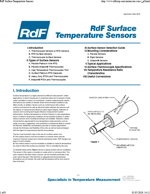
To illustrate these points Figure I shows a typical surface sensor installation. The sensor in this case is mounted on a pipe which is carrying a fluid. The point closest to the fluid where a sensor can be mounted practically is the outer wall of the pipe. If the fluid flow is adequate and the temperature fluctuations are not severe, the outer wall temperature will be very close to that of the fluid.
–200°C to +232°C (–320°F to +450°F) –200°C to260°C (–320°F to +500°F)
Thermocouple Types K, E, T or J* Grounded or Ungrounded
Resistance 100 Ω or 1000 Ω Platinum @0°C
百为STM32开发板用户手册
兼容STM3210E-EV AL开发板采用STM32F103ZET6微控制器,带USB2.0,CAN2.0A/B,I2S,I2C,USART,SPI,DAC,FSMC,SDIO,64KB SRAM,512KB Flash,JTAG和SWD仿真下载接口。
软件代码和硬件电路兼容官方STM3210E-EV AL开发板,支持UCOS,uCLinux操作系统。
一、百为STM32开发板概述:1、硬件特性:l 两种供电方式,外部5V供电和USB供电方式l 三种启动模式,下载模式、用户程序模式、内部SRAM启动模式l AK4642 I2S音频DAC,立体声耳机l MicroSD卡接口l 8Mbit SPI FLASH,1MB SRAM,128Mbit NOR Flash,64MB NAND Flashl I2C接口温度传感器芯片LM75Al 两个串口,其中一个带RTS/CTS控制l USB2.0 device接口l CAN2.0A/B兼容接口l JTAG仿真调试下载接口l 240x320 TFT彩屏l 五向游戏杆控制l 复位按键l 4个LED指示灯l RTC电池备份l 全部IO通过双排插针引出l BNC接口2、软件特性:l 简单不带库例程l 官方带库例程l 支持ST官方DEMO程序l 支持UCOS2.86+UCGUI3.90+ILI9320+TSC2046触摸l 支持FATFS+SDIO+helix软解码MP3l uCLinux操作系统l ST GUI库二、开发板硬件框图:硬件模块图:实物功能对照图:CONNETORSTM32F103ZET6SPI FLASHBOOT SELECTAK4642TF CARDAUDIO JACKADC INPUT开发板提供外部5V供电及USB供电两种方式,可通过JP13跳帽选择任意一种。
l 外部5V供电方式,JP13跳帽接PSUl USB供电方式,JP13跳帽接USB,默认USB供电方式l JP1连接1、2,VBAT接到备份电池l JP1连接2、3,VBAT接到3.3V2、启动方式l 从用户FLASH启动l 从系统存储器启动l 从内部SRAM启动开发板上有两种时钟源l X2,32KHz晶振作为RTC时钟源l X1,8MHz晶振作为MCU的时钟源,当使用内部RC震荡器作为时钟源时,可以将8MHz 晶振去掉4、复位方式STM32复位为低电平有效,开发板上有三种复位方式:l 上电复位l 通过开发板上的RESET按键复位l JTAG调试器输入复位信号5、音频AK4642音频芯片连接到STM32F103ZET6的I2S2接口,支持立体声耳机接口输出。
- 1、下载文档前请自行甄别文档内容的完整性,平台不提供额外的编辑、内容补充、找答案等附加服务。
- 2、"仅部分预览"的文档,不可在线预览部分如存在完整性等问题,可反馈申请退款(可完整预览的文档不适用该条件!)。
- 3、如文档侵犯您的权益,请联系客服反馈,我们会尽快为您处理(人工客服工作时间:9:00-18:30)。
STM32V100评估板用户手册
V1.0
第一章:概述
STM103V100是英蓓特公司新推出的一款基于ST意法半导体STM32系列处理器(Cortex-M3内核)的全功能评估板。
STM103V100评估板有USB,Motor Control ,CAN,SD卡,Smart 卡,UART 等丰富的外设,有助于用户评估STM32的性能。
STM103V100评估板支持JTAG和SWD串行调试方式,非常方便。
STM103V100评估板主要性能:
◆处理器:STM32F103VBT6
◆RTC
◆8M byte SPI Flash
◆启动跳线设置
◆将所有的通过排针引脚引出,
◆3路可选电源,分别是外接5VDC供电,USB供电,引出排针接入供电,
◆一个SD存储卡接口
◆TFT LCD和16x2字符型液晶接口
◆外扩一个温度传感器
◆一个电机接口
◆两种类型调试接口,可选10pin SWD接口或20Pin JTAG接口
◆2个RS232串行口,其中一个支持RTS/CTS功能
◆一个USB Slave B型接口
◆一个可以具有控制四个方向和确定功能的摇杆手柄
◆四个按键分别是Reset,Wakeup,Temper和User按键
◆四个Led灯
◆一路立体声音频输出接口,一路麦克风接口
◆一个CAN总线接口,通过DB9接口引出
第二章:STM103V100X硬件介绍
STM103V100功能模块图如下图所示:
2.1接口一览表CAN
JTAG
调节声音大小电位器
耳机插孔
AD输入旋钮
五维摇杆按键
外接直流电源接口
2.2电源
STM32评估板有三种供电方式,通过JP11选择以下其中一种方式供电。
1. 通过主板电源端子J1输入5VDC。
2. 通过主板上USB 端口(CN1)供电,供电电流小于5oomA.。
3. 通过外接排针CN12,从外板供电。
主板上DC5V输入端子(CN4)信号为内正外负,如下图所示:
2.3启动方式选择
STM32评估板有以下三种启动方式:
■从用户闪存存储器启动
■从系统存储器启动
■从内嵌SRAM启动
通过设置子板上拨动开关SW1 和SW2选择启动方式
2. 4时钟源
STM32评估板上有两种时钟源:
■32KHz 晶振作为RTC的时钟源
■8MHz晶振作为MCU的时钟源,当使用内部RC时钟作为时钟源的时候,可以把8MHz晶振拔掉。
2.5 复位方式
STM32评估板有三种复位方式:
■通过子板上的复位按键B5复位
■如果短接JP10,可通过JTAG调试口输入复位信号
■通过外接排针CN13,从外板输入复位信号
2.6音频
STM32评估板有录音和回放功能。
通过条线JP6设置禁止和使能,通过可调电阻RV2调整声音大小,通过RV3调整麦克风的增益。
2.7串行flash
STM32评估板子板上外扩了64Mbit的串行SPI flash。
与SD卡共用SPI通信端口,使用不同的片选,此FLASH的片选是被PA4口控制。
2.8串口
STM32开发板引出了两路UART,UART1(CN11)和UART2(CN6)。
两路串口均连接到公的DB9连接头。
UART2支持RTS/CTS握手信号。
UART2RS232 DB9公连接头信号定义:
UART1 RS232 DB9连接头信号定义:
2.9电机控制接口
STM32开发板上有一个34pin的感应电机控制接口,该接口提供驱动板所需的控制信号,并从驱动板接收回馈信号。
这些信号包括紧急停止信号,调速信号,六路PWM控制信号,以及从驱动板反馈回来的三相电机电流,母线电压,散热器温度等信号。
电机控制接口CN14接口图:
信号定义:
2.10 Smart Card接口
通过Smart card接口芯片ST8024,STM32评估板可支持3V 和5V 的smart 卡。
ST8024和STM32评估板的接口连接信号如下:
2.11 SD卡接口
STM32评估板具有SD卡接口,支持SD卡的读写。
SD卡和STM32接口的连接信号如下:
2.12 CAN 接口
STM32 板上使用SN65HVD230 (U5) 作为CAN 驱动器。
CAN接口采用DB9链接器接线,这里针2 提供CANL 信号,针7 提供CANH信号.这些针连接到SN65HVD230 CAN 驱动器芯片。
CAN DB9连接器引脚定义:
2.13 温度传感器
I2C接口的温度传感器STLM75连接到STM32开发板的I2C1接口上,两个分立的N通道增强型MOS-FET用于转换电平,使得不同电压的器件能接入到同一I2C总线上的。
2.14模拟输入
BNC接头
2.15 IrDA
STM32开发板支持红外接收,STM32评估板上的IrDA 接收器连接到的UART3上,可以通
2.16 USB
STM32支持USB2.0,通过STM32评估板上的USB B型口(CN1)可进行USB全速通讯,也可以通过该USB口给STM32评估板提供5VDC(500mA限流)。
2.17调试接口
STM32评估板有二种调试接口:
■CN7,标准的20脚JTAG仿真调试接口,
■CN9,10针SWD调试接口,支持新的ARM Cortex-M3串行调试功能
JTAG调试接口定义如下:
SWD调试接口CN9接口定义
2.18人机界面(LCD)接口
第三章软件开发和相关例程
3.1 MDK介绍
RealView MDK开发套件是ARM公司目前最新推出的针对各种嵌入式处理器的软件开发工具。
RealView MDK集成了业内最领先的技术,包括μVision3集成开发环境与RealView编译器。
支持ARM7、ARM9和最新的Cortex-M3核处理器,自动配置启动代码,集成Flash
烧写模块,强大的Simulation设备模拟,性能分析等功能。
MDK 软件可以从STM32评估板配套光盘获取,或者从Keil网站中下载最新版本。
双击安装文件setup.exe,出现如下的安装界面,根据界面安装向导的提示,完成Keil u Vision3的安装。
3.2例程介绍
STM32
3.3
程序例程操作顺序(例LCD_1620字符显示实验)
1.首先打开LCD_1620文件夹(里面有三个文件夹:uvision-存放工程文件和源文件,obj-存放编译文件,listing-存放链接及印像文件),进入uvision文件夹中双击LCD_char.Uv2工程文件,则会打开工程文件。
2.工程文件中包含Start Up(启动代码存放区),Source Code(主要的源程序代码存放区),Library(源程序文件库),Document(程序的说明文档)文件夹。
3.连接好电源线和仿真器接线(外接仿真器连接线(JTAG))
4.点击Flash/Download进行程序下载:如图
或者点击快捷图标:
5.下载完后可执行Debug/Start/Stop Debug Session(Ctrl+F5)进行调试,如图:
或者快捷图标:来进行调试。
点击以后主显示区显示汇编程序代码,要查看源代码可以在单步之前右击鼠标选择Show Source Code for current Address.如下图:
点击下载程序
将会显示程序的源代码。
6.利用窗口上的快捷调试图标来执行调试过程,图标如下:
附录A:STM32评估板IO分配
附录B:售后服务。