友达光电的生产线布局 100416
全球第五代和第六代TFT-LCD生产线概况
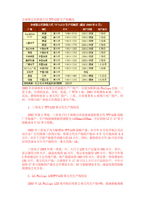
全球第五代和第六代TFT-LCD生产线概况2003年全球将有8座第五代面板生产厂投产,分别为韩国LG.Philips 2座、三星2座,台湾的友达、奇美、彩晶、广辉等4座。
2004年将增加6座,其中,友达、群创科技各1 座五代厂投产,三星、日本夏普各1座第六代厂投产,同时,中国大陆厂商也正在规划2条生产线。
1、三星电子TFT-LCD第五代生产线状况2002年第2季度,三星电子位于南韩公州忠清南道的第五代TFT-LCD面板厂开始量产。
生产线玻璃基板的规格为1100mmx1250mm,可以切割12片17英寸面板或6片24英寸面板。
2003年三星电子为大幅增加TFT-LCD面板产量,从今年5月份开始正式启动天安厂五代线第三阶段计划,将第五代生产线的产量由5.5万片提高到 6.8万片,并在7月将产能提升到最大的10万片。
同时,最快将从今年10月份开始启用具备6万片月产能的另一条五代线-L6。
三星电子2003年第一季度,中、大尺寸LCD生产总量为336万片,其中,显示器用170万片、液晶电视用16万片、笔记本电脑用150万片。
预计今年第2季度通过扩大五代线产能,将产量提高到460-470万片,将比第一季度增加约130万片。
第五代生产线,主要将扩大17英寸以上大尺寸产品的生产,今年计划将17英寸面板的产量比去年增加3倍,19寸面板增加5倍,液晶电视用面板则增加2至3倍。
2、LG.Philips LCDTFT-LCD第五代生产线状况2003年LG.Philips LCD将开始启用第2座五代生产线-P5,玻璃基板规格为1100×1250mm,上半年月产量3万片,并逐步增加到6万片。
同时,计划在2003年底,将五代线整体月产能增加到12万片(含P4的6万片)。
该条生产线适用于最近需求激增的17英寸显示器用面板,每片基板可生产12片17英寸面板,将有助于缓解目前供货紧张的局面。
同时,随着第二条五代线的启用,该公司的五代线将具备15英寸、17英寸、Wide18.1英寸与19英寸显示器用TFT-LCD,以及26英寸、30英寸Wide与42英寸电视用TFT-LCD等多样化产品线,可灵活地应对各种客户的需求。
TFT-LCD生产线简介 PPT
京东方第10.5代TFT-LCD生产线
• 京东方400亿10.5代线拟于2018年第三季投产,据京东方2015年7月 12日(00725.SZ)发布在合肥第10.5代线液晶面板生产线,将在 2015年第四季度前开工,这将是全球第一条10.5代线,此前全球高世 代线的液晶面板生产线为夏普在日本的10代线。
• 2010年9月3日,“中国内地首条第6代TFT-LCD生产线产品点亮仪式” 在合肥京东方光电科技有限公司正式举行。标志着京东方合肥6代线 正式进入试生产,也标志着中国液晶显示产业有了新的突破,迎来 了一个重要的历史时刻。从此,彻底结束了32英寸以上液晶电视无 国产屏的历史,将中国电子信息产业的 “中国创造”水平提升到一 个新台阶。
•TFT-LCD相比传统的彩色显像管(CRT),具有轻、薄、低辐射、环保 等优点,从而广泛应用于电脑显示器、笔记本电脑、液晶电视、移动电 话等领域,是当今平板显示技术的主流发展方向,也是未来20年内电子 信息产业增长的核心动力。
• 全球第l、2代TFT-LCD生产线全部用于小尺寸产品生产,这些生产线 已建了12~15年,设备老化,未来3年左右时间将逐步退出市场,或 关闭、或转做研发和人员培训。
• 5代线不仅是技术实验基地,还是人才培训基地。从2005年开始到现 在,京东方已经在这条线上培养了2000多名核心技术人员和工程人 员,这些人后来都成为了京东方建设4.5代线、6代线和8.5代线的技 术主力。
京东方第六代TFT-LCD生产线
• 数据显示,液晶显示屏占液晶电视制造成本的70%以上。中国作为液 晶显示屏消费大户,一直以来始终处于整机制造末端。内地液晶显 示屏高度依赖进口,而32英寸以上液晶电视屏则全部依赖进口。
LCD生产线简介
一 TFT-LCD生产线的演进
5代线及5代线以上的TFT-LCD生产线主要用于生产主流大尺 寸液晶面板。受基板尺寸和经济切割的限制,不同世代线均 有各自的产品定位。 第5代线主要针对26英寸以下的产品,市场定位在15英寸、 17英寸和19英寸显示器和笔记本电脑面板以及22英寸、27英 寸的液晶电视。 第6代线主要针对37英寸及以下的面板,主要用于32英寸和 37英寸液晶电视。 第7代线主要针对40英寸以上液晶电视,以切割生产40英寸 和46英寸面板为主。 8代线以上则主要针对50英寸以上的超大液晶电视面板。
日本液晶显示产业发展研究
进入21世纪后,随着韩国和中国台湾在液晶显示领 域的崛起,日本厂商在生产线上投入相对这两个地 区较少,随着韩国和台湾厂商在液晶显示制造业上 的扩大,日本的液晶显示相关技术也转移到这些地 区,但一些高端不容易被制造的面板所需关键材料、 化学用品和电子材料等仍主要掌握在日本厂商手中。 产业政策及支持 日本液晶显示技术之所以能够做大做强,与政府的 政策扶持以及资金支持是分不开的。日本很早就把 发展光电子上升为“国家发展战略”,有力地推动 了新型平板显示器件产业的发展。
三 全世界范围LCD的生产
京东方之前,世界上TFT-LCD的生产和研发主要被韩 国、台湾地区和日本厂商所垄断。 TFT-LCD产品市 场也基本上被这三地的企业所分割,这些企业对技 术控制相当严格。
2006年第3季度10大液晶 电视制造商市场份额
日本液晶显示产业发展研究
日本是液晶显示技术发展的主要创造者与推 动者之一,液晶显示技术最早源于美国,但 将这个技术产业化的是日本。发展至今,日 本在液晶显示技术方面一直处于领先地位, 垄断了液晶显示上游的材料技术。 日本的科研机构和企业是世界上最先察觉到 液晶显示技术具有广泛应用前景的。
图南光电,友达M170ETN01_1规格书

图南光电 http://www.tndisplay.com.cnProduct SpecificationAU OPTRONICS CORPORATIONM170ETN01.1(V ) Preliminary Specification ( ) Final Specification Module Model Name 17” Color TFT-LCD M170ETN01.1CustomerDateApproved byDateChi Yin WuFeb 6, 2013Approved byPrepared byDateJia Hau JeanFeb 6, 2013Note: This Specification is subject to change without notice.AU Optronics corporationdocument version 0.01图南光电 http://www.tndisplay.com.cnProduct SpecificationAU OPTRONICS CORPORATIONM170ETN01.1Contents 1 Handling Precautions................................................................4 2 General Description ..................................................................52.1 Display Characteristics....................................................................................................... 5 2.2 Absolute Maximum Rating of Environment ........................................................................ 6 2.3 Optical Characteristics ....................................................................................................... 73 TFT-LCD Module ......................................................................113.1 Block Diagram.................................................................................................................. 11 3.2 Interface Connection........................................................................................................ 12 3.2.1 Connector Type....................................................................................................... 12 3.2.2 Connector Pin Assignment...................................................................................... 12 3.3 Electrical Characteristics.................................................................................................. 14 3.3.1 Absolute Maximum Rating ...................................................................................... 14 3.3.2 Recommended Operating Condition....................................................................... 14 3.4 Signal Characteristics ...................................................................................................... 15 3.4.1 LCD Pixel Format.................................................................................................... 15 3.4.2 LVDS Data Format .................................................................................................. 15 3.4.3 Color versus Input Data .......................................................................................... 16 3.4.4 LVDS Specification.................................................................................................. 17 3.4.5 Input Timing Specification ....................................................................................... 19 3.4.6 Input Timing Diagram .............................................................................................. 20 3.5 Power ON/OFF Sequence ............................................................................................... 214 Backlight Unit .........................................................................224.1 Block Diagram.................................................................................................................. 22 4.2 Interface Connection........................................................................................................ 23 4.2.1 Connector Type....................................................................................................... 23 4.2.2 Connector Pin Assignment...................................................................................... 25 4.3 Electrical Characteristics.................................................................................................. 26 4.3.1 Absolute Maximum Rating ...................................................................................... 26 4.3.2 Recommended Operating Condition....................................................................... 265 6 7 8Reliability Test ........................................................................28 Shipping Label ........................................................................29 Mechanical Characteristics .....................................................30 Packing Specification..............................................................318.1 Packing Flow.................................................................................................................... 31 8.2 Pallet and shipment information....................................................................................... 32document version 0.02图南光电 http://www.tndisplay.com.cnProduct SpecificationAU OPTRONICS CORPORATIONM170ETN01.1Record of RevisionVersion Date Page Old description New Description Remark0.02013/2/6AllFirst version release-document version 0.03Product SpecificationAU OPTRONICS CORPORATIONM170ETN01.11 Handling Precautions 1) 2) 3) 4) 5) 6) 7) 8) 9) Since front polarizer is easily damaged, pay attention not to scratch it. Be sure to turn off power supply when inserting or disconnecting from input connector. Wipe off water drop immediately. Long contact with water may cause discoloration or spots. When the panel surface is soiled, wipe it with absorbent cotton or other soft cloth. Since the panel is made of glass, it may break or crack if dropped or bumped on hard surface. Since CMOS LSI is used in this module, take care of static electricity and insure human earth when handling. Do not open or modify the Module Assembly. Do not press the reflector sheet at the back of the module to any directions. In case a TFT-LCD Module has to be put back into the packing container slot after once it was taken out from the container, do not press the center of the LED lightbar edge. Otherwise the TFT-LCD Module may be damaged. Insert or pull out the interface connector, be sure not to rotate nor tilt it of the TFT-LCD Module. Do not twist nor bend the TFT -LCD Module even momentary. It should be taken into consideration that no bending/twisting forces are applied to the TFT-LCD Module from outside. Otherwise the TFT-LCD Module may be damaged. Please avoid touching COF position while you are doing mechanical design. When storing modules as spares for a long time, the following precaution is necessary: Store them in a dark place. Do not expose the module to sunlight or fluorescent light. Keep the temperature between 5℃ and 35℃ at normal humidity.10) 11)12) 13)document version 0.04Product SpecificationAU OPTRONICS CORPORATIONM170ETN01.12 General Description This specification applies to the 17 inch wide Color a-Si TFT-LCD Module M170ETN01.1. The display supports the SXGA+ (1280(H) x 1024(V)) screen format and 16.7M colors (RGB 6-bits + Hi-FRC data). The input interface is Dual channel LVDS and this module doesn’t contain an driver board for backlight.2.1 Display Characteristics The following items are characteristics summary on the table under 25℃ condition:ITEMS Screen Diagonal Active Area Pixels H x V Pixel Pitch Pixel Arrangement Display Mode White Luminance ( Center ) Contrast Ratio Response Time Power Consumption (LCD Module + Backligh unit) Weight Outline Dimension Electrical Interface Support Color Surface Treatment Temperature Range Operating Storage (Shipping) RoHS Compliance TCO Compliance Unit [mm] [mm] [mm] [cd/m2] [msec] [Watt] SPECIFICATIONS 432 (17.0”) 337.920(H) × 270.336(V) 1280 × 3(RGB) × 1024 0.264(per one triad) × 0.264 R.G.B. Vertical Stripe Normally White 250 (Typ.) 1000 : 1 (Typ.) 5 (Typ., on/off) 9.91 (Typ.) LCD module : PDD (Typ.)=3 @ Black pattern,Fv=60Hz Backlight unit : PBLU (Typ.) =6.91 @Is=60mA 1273 (Typ.) 358.5(H) x 296.5(V) x 10.3(D) (Typ.) Dual Channel LVDS 16.7M colors (RGB 6-bits +Hi-FRC data) Anti-glare type, Hardness 3H 0 to +50 -20 to +60 RoHS Compliance TCO6.0 Compliance[Grams] [mm] [oC] [oC] -document version 0.05Product SpecificationAU OPTRONICS CORPORATIONM170ETN01.12.2 Absolute Maximum Rating of Environment Permanent damage may occur if exceeding the following maximum rating. Symbol TOP TGS HOP TST HST Description Operating Temperature Glass surface temperature (operation) Operation Humidity Storage Temperature Storage Humidity Min. 0 0 5 -20 5 Max. +50 +65 90 +60 90 Unit [ C] [ C] [%RH] [oC] [%RH]o oRemark Note 2-1 Note 2-1Function judged onlyNote 2-1Note 2-1: Temperature and relative humidity range are shown as the below figure. 1. 90% RH Max ( Ta ≦39℃) 2. Max wet-bulb temperature at 39℃ or less. ( Ta ≦39℃) 3. No condensationOperating RangeStorage Rangedocument version 0.06Product SpecificationAU OPTRONICS CORPORATIONM170ETN01.12.3 Optical Characteristics The optical characteristics are measured on the following test condition. Test Condition: 1. Equipment setup: Please refer to Note 2-2. 2. Panel Lighting time: 30 minutes 3. VDD=5.0V, Fv=60Hz,Is=60mA,Ta=25℃Symbol Description White Luminance (Center of screen) Min. 200 75 600 75 75 70 70 75 75 70 70 TBD TBD TBD TBD TBD TBD Typ. 250 80 1000 85 85 80 80 88 88 85 85 3.8 1.2 5 TBD TBD TBD TBD TBD TBD Max. 5.5 2.5 8 TBD TBD TBD TBD TBD TBD By SR-3 [msec] Note 2-6 By TRD-100 [degree] Note 2-5 By SR-3 Unit[cd/m2]Remark Note 2-2 By SR-3 Note 2-3 By SR-3Lw Luni CR θR θL ΦH ΦL θR θL ΦH ΦL TR TF Rx Ry Gx Gy Bx By Wx Wy CT FdBLuminance Uniformity (9 points) Contrast Ratio (Center of screen) Horizontal Viewing Angle (CR=10) Vertical Viewing Angle (CR=10) Horizontal Viewing Angle (CR=5) Vertical Viewing Angle (CR=5) Right Left Up Down Right Left Up Down Rising Time Response Time Falling Time Rising + Falling Red x Red y Green x Color Coordinates (CIE 1931) Green y Blue x Blue y White x White y Crosstalk Flicker (Center of screen)[%]-Note 2-4 By SR-30.283 0.313 0.343 0.299 0.329 0.359 1.5 -20 [%] [dB] Note 2-7 By SR-3 Note 2-8 By SR-3document version 0.07Product SpecificationAU OPTRONICS CORPORATIONM170ETN01.1Note 2-2: Equipment setup :Photo detector (SR-3, TRD-100)Measured distance (50cm)LCD PanelTFT-LCD ModuleCenter of the screen Note 2-3: Luminance Uniformity Measurement Definition:Luminance Uniformity =Minimum Luminance of 9 Points (P1 ~ P9) Maximum Luminance of 9 Points (P1 ~ P9)a.Test pattern: White Patterndocument version 0.08Product SpecificationAU OPTRONICS CORPORATIONM170ETN01.1Note 2-4: Contrast Ratio Measurement Definition:Contrast Ratio =Luminance of White pattern Luminance of Black patterna. Measured position: Center of screen (P5) & perpendicular to the screen (θ=Φ=0°) Note 2-5: Viewing angle measurement Definition: The angle at which the contrast ratio is greater than 10 & 5 . a. Horizontal view angle: Divide to left & right (θL & θR) Vertical view angle: Divide to up & down (ΦH &ΦL)Note 2-6: Response time measurement The output signals of photo detector are measured when the input signals are changed from “Black” to “White” (rising time, TR), and from “White” to “Black” (falling time, TF), respectively. The response time is interval between the 10% and 90% of optical response. (Black & White color definition: Please refer section 3.4.3)%TFTR100 90 Optical response 10 0 1 Frame 1 Frame White Black B lack W hitedocument version 0.09Product SpecificationAU OPTRONICS CORPORATIONM170ETN01.1Note 2-7: Crosstalk measurement Definition: CT = Max. (CTH,CTV); Where a.Maximum Horizontal Crosstalk : CTH = Max. (| YBL – YAL | / YAL × 100 %, | YBR – YAR | / YAR × 100 %); Maximum Vertical Crosstalk: CTV = Max. (| YBU – YAU | / YAU × 100 %, | YBD – YAD | / YAD × 100 %); b. YAU, YAD, YAL, YAR = Luminance of measured location without Black pattern YBU, YBD, YBL, YBR = Luminance of measured location with Black patternNote 2-8: Flicker measurement a. Test pattern: It is listed as following. Gray level = L0Gray level = L127R: Red, G: Green, B:Blue b. Measured position: Center of screen (P5) & perpendicular to the screen (θ=Φ=0°)document version 0.010Product SpecificationAU OPTRONICS CORPORATIONM170ETN01.13 TFT-LCD Module 3.1 Block Diagram The following shows the block diagram of the 17 inch Color TFT-LCD Module.ConnectorLVDS Signal Signal VDDDC/DCConverterGamma Correction G1 D1 X-Driver IC D3840AUO ASICTiming Controller Mini LVDS TransmitterTFT-LCD1280(x3) x 1024 Pixels G1024LVDSReceiverASIC Control Boarddocument version 0.011Product SpecificationAU OPTRONICS CORPORATIONM170ETN01.13.2 Interface Connection 3.2.1 Connector Type Manufacturer Part Number Mating Connector Manufacturer Part Number P-TWOAL230F-A0G1D-PTFT-LCD ConnectorSTMMSCKT2407P30HBJAEFI-XB30SSRLAHF16JAE FI-X30HL (Locked Type)3.2.2 Connector Pin Assignment PIN # 1 2 3 4 5 6 7 8 9 10 11 12 13 14 15 16 17 18 19 20 21 22 23 24 25 26 Symbol RxO0RxO0+ RxO1RxO1+ RxO2RxO2+ GND RxOCLKRxOCLK+ RxO3RxO3+ RxE0RxE0+ GND RxE1RxE1+ GND RxE2RxE2+ RxECLKRxECLK+ RxE3RxE3+ GND NC NC Description Negative LVDS differential data input (Odd data) Positive LVDS differential data input (Odd data) Negative LVDS differential data input (Odd data) Positive LVDS differential data input (Odd data) Negative LVDS differential data input (Odd data) Positive LVDS differential data input (Odd data) Ground Negative LVDS differential clock input (Odd clock) Positive LVDS differential clock input (Odd clock) Negative LVDS differential data input (Odd data) Positive LVDS differential data input (Odd data) Negative LVDS differential data input (Even data) Positive LVDS differential data input (Even data) Ground Negative LVDS differential data input (Even data) Positive LVDS differential data input (Even data) Ground Negative LVDS differential data input (Even data) Positive LVDS differential data input (Even data) Negative LVDS differential clock input (Even clock) Positive LVDS differential clock input (Even clock) Negative LVDS differential data input (Even data) Positive LVDS differential data input (Even data) Ground No connection (for AUO test only. Do not connect) No connection (for AUO test only. Do not connect)12Remarkdocument version 0.0Product SpecificationAU OPTRONICS CORPORATIONM170ETN01.127 28 29 30NC VDD VDD VDDNo connection (for AUO test only. Do not connect) Power Supply Input Voltage Power Supply Input Voltage Power Supply Input Voltagedocument version 0.013Product SpecificationAU OPTRONICS CORPORATIONM170ETN01.13.3 Electrical Characteristics 3.3.1 Absolute Maximum Rating Permanent damage may occur if exceeding the following maximum rating. Symbol VDD Description Power Supply Input Voltage Min GND-0.3 Max 6.0 Unit [Volt] Remark Ta=25℃3.3.2 Recommended Operating Condition Symbol VDD IDD PDD IRush VDDrp Description Power supply Input voltagePower supply Input Current (RMS)Min 4.5 -Typ 5.0 0.6 0.72 3 3.6Max 5.5 0.72 0.87 3.6 4.32 3.0 500Unit [Volt] [A] [A]RemarkVDD= 5.0V, Black Pattern, Fv=60Hz VDD= 5.0V, Black Pattern, Fv=75HzVDD Power Consumption Inrush Current Allowable VDD Ripple Voltage[Watt] VDD= 5.0V, Black Pattern, Fv=60Hz [Watt] VDD= 5.0V, Black Pattern, Fv=75Hz [A] Note 3-1--[mV] VDD= 5.0V, Black Pattern, Fv=75HzNote 3-1: Inrush Current measurement: Test circuit:The duration of VDD rising time: 470us.document version 0.0 14Product SpecificationAU OPTRONICS CORPORATIONM170ETN01.13.4 Signal Characteristics 3.4.1 LCD Pixel Format1 1st Line 2 1279 1280 R G B R G BR G B R GB1024th Line R G B R G BR G B R G B3.4.2 LVDS Data FormatNote 3-2: a. O = “Odd Pixel Data” E = “Even Pixel Data” nd b. Refer to 3.4.1 LCD pixel format, the 1st data is 1 (Odd Pixel Data), the 2 data is 2 (Even Pixel Data) and the last data is 1280 (Even Pixel Data).document version 0.015Product SpecificationAU OPTRONICS CORPORATIONM170ETN01.13.4.3 Color versus Input Data The following table is for color versus input data (8bit). The higher the gray level, the brighter the color.document version 0.016Product SpecificationAU OPTRONICS CORPORATIONM170ETN01.13.4.4 LVDS Specification a. DC Characteristics: Symbol VTH VTL │VID│ VCM Description LVDS Differential Input High Threshold LVDS Differential Input Low Threshold LVDS Differential Input Voltage LVDS Common Mode Voltage Min -100 100 +1.0 Typ +1.2 Max +100 600 +1.5 Units [mV] [mV] [mV] [V] VTH-VTL = 200mV Condition VCM = 1.2V VCM = 1.2VLVDS Signal Waveform: Use RxOCLK- & RxOCLK+ as example.RxOCLK-RxOCLK+document version 0.017Product SpecificationAU OPTRONICS CORPORATIONM170ETN01.1b. AC Characteristics: Symbol Description Maximum deviation of input clock frequency during Spread Spectrum FMOD Maximum modulation frequency of input clock during Spread Spectrum 200 KHz Min Max Unit RemarkFDEV-±3%Freq Fmax Fclk * FDEV Fclk Fmin 1 FMOD < Spread Spectrum> TimeFclk: LVDS Clock Frequencydocument version 0.018Product SpecificationAU OPTRONICS CORPORATIONM170ETN01.13.4.5 Input Timing Specification It only support DE mode, and the input timing are shown as the following table. Symbol Tv Tdisp (v) Tblk (v) Fv Th Tdisp (h) Tblk (h) Fh Tclk Fclk LVDS Clock Horizontal Section Vertical Section Description Period Active Blanking Frequency Period Active Blanking Frequency Period Frequency Min. 1036 1024 12 50 730 640 90 37.8 50 51.8 Typ. 1066 1024 42 60 844 640 204 54 60 64 Max. 1873 1024 849 76 1320 640 680 68.4 76 93.7 Unit Th Th Th Hz Tclk Tclk Tclk KHz ns MHz Note 3-3 1/Fclk Note 3-4 RemarkNote 3-3: The equation is listed as following. Please don’t exceed the above recommended value. Fh (Min.) = Fclk (Min.) / Th (Min.); Fh (Typ.) = Fclk (Typ.) / Th (Typ.); Fh (Max.)= Fclk (Max.) / Th (Min.); Note 3-4: The equation is listed as following. Please don’t exceed the above recommended value. Fclk (Min.) = Fv (Min.) x Th (Min.) x Tv (Min.); Fclk (Typ.) = Fv (Typ.) x Th (Typ.) x Tv (Typ.); Fclk (Max.) = Fv (Max.) x Th (Typ.) x Tv (Typ.);document version 0.019Product SpecificationAU OPTRONICS CORPORATIONM170ETN01.13.4.6 Input Timing DiagramTv M pixel Tblk(v) Tdisp(v) Y Th N LineXDEN RGB DataLineInvalid Data1Line2Line3Line4LineNLineInvalid DataCLKTclkThTdisp(h)Tblk(h)DERGB Data Pixel Pixel Pixel Pixel (Odd) M-7 M-5 M-3 M-1Invalid DataPixel Pixel Pixel Pixel Pixel Pixel 1 3 5 7 9 11Pixel Pixel Pixel M-5 M-3 M-1Invalid DataPixel Pixel 1 3RGB Data Pixel Pixel Pixel Pixel (Even) M-6 M-4 M-2 MInvalid DataPixel Pixel Pixel Pixel Pixel Pixel 2 4 6 8 10 12PixelPixel M-4PixelM-2 MInvalid DataPixel Pixel 2 4document version 0.020Product SpecificationAU OPTRONICS CORPORATIONM170ETN01.13.5 Power ON/OFF Sequence VDD power,LVDS signal and backlight on/off sequence are as following. LVDS signals from any system shall be Hi-Z state when VDD is off.Backlight OffT190% 90% 10%VDD10%T2T5T6T7LVDS SignalVALID DATA T3 T4 Backlight On Backlight OffVSLEDBacklight OffPower Sequence TimingSymbol Min.T1 T2 T3 T4 T5 T6 T7 0.5 0 500 100 0 0 1000Value Typ.-Max.10 50 50Unit[ms] [ms] [ms] [ms] [ms] [ms] [ms]RemarkNote 3-5 Note 3-6 Note 3-6-150 -Note 3-5 : Recommend setting T5 = 0ms to avoid electronic noise when VDD is off. Note 3-6 : During T5 and T6 period , please keep the level of input LVDS signals with Hi-Z state.document version 0.021Product SpecificationAU OPTRONICS CORPORATIONM170ETN01.14 Backlight Unit 4.1 Block Diagram The following shows the block diagram of the 17 inch Backlight Unit. And it includes 36 pcs LED in the LED light bar. (4 strings and 9 pcs LED of one string).+ VS -ISISISISConnectorVSLEDCh1Ch2Ch3Ch4document version 0.022Product SpecificationAU OPTRONICS CORPORATIONM170ETN01.14.2 Interface Connection 4.2.1 Connector Type Manufacturer Backlight Connector Part Number Manufacturer Mating Connector Part Number H112K-P06N-13B (Locking type) 3707K-S06N-21R ENTERY ENTERYBacklight Connector dimension:H × V × D = 13.9 × 3.00 × 4.25, Pitch = 1.0(unit = mm )document version 0.023Product SpecificationAU OPTRONICS CORPORATIONM170ETN01.1Mating Connector dimension:document version 0.024Product SpecificationAU OPTRONICS CORPORATIONM170ETN01.14.2.2 Connector Pin Assignment Pin# 1 2 3 4 5 6 Symbol Ch1 Ch2 VSLED VSLED Ch3 Ch4 Description LED Current Feedback Terminal (Channel 1) LED Current Feedback Terminal (Channel 2) LED Power Supply Voltage Input Terminal LED Power Supply Voltage Input Terminal LED Current Feedback Terminal (Channel 3) LED Current Feedback Terminal (Channel 4) RemarkPIN1document version 0.025Product SpecificationAU OPTRONICS CORPORATIONM170ETN01.14.3 Electrical Characteristics 4.3.1 Absolute Maximum RatingPermanent damage may occur if exceeding the following maximum rating. (Ta=25 ) Remark100% duty ratio Duty ratio 10% Pulse time=10 msSymbol IsDescription LED String CurrentMin 0Max 90 150Unit [mA] [mA]℃≦Duty ratio= (A / B) X 100% ;(A: Pulse time, B: Period)4.3.2 Recommended Operating Condition (Ta=25℃)Symbol Description Min. Typ. Max. Unit Remark 100% duty ratio of LED chip Is=60mA @ 100% duty ratio; Note 4-1 Is=60mA @ 100% duty ratio; Note 4-2Is Vs ∆Vs PBLU LTLEDLED String Current LED String Voltage Maximum Vs Voltage Deviation of light bar LED Light Bar Power Consumption LED Life Time25.260 28.8 6.91 -66 32.4 1.8 8.55 -[mA] [Volt] [Volt] [Watt] [Hour]30,000Note 4-3 Note 4-4document version 0.026Product SpecificationAU OPTRONICS CORPORATIONM170ETN01.1Note 4-1: Vs (Typ.) = VF (Typ.) X LED No. (one string); a. VF: LED chip forward voltage, VF (Min.)=2.8V, VF(Typ.)=3.2V, VF(Max.)=3.6V b. The same euqation to calculate Vs(Min.) & Vs (Max.) for respective VF (Min.) & VF(Max.);Note 4-2: ∆Vs (Max.) = ∆VF X LED No. (one string); a. ∆VF: LED chip forward voltage deviation; (0.2 V , each Bin of LED VF) Note 4-3: PBLU (Typ.) = Vs (Typ.) X Is (Typ.) X 4 ; ( 4 is total String No. of LED Light bar) PBLU (Max.) = Vs (Max.) X Is (Max.) X 4 ; Note 4-4: Definition of life time: a. Brightness of LED becomes to 50% of its original value b. Test condition: Is = 60mA and 25℃ (Room Temperature)document version 0.027Product SpecificationAU OPTRONICS CORPORATIONM170ETN01.15 Reliability Test AUO reliability test items are listed as following table. (Bare Panel only) ItemsTemperature Humidity Bias (THB) High Temperature Operation (HTO) Low Temperature Operation (LTO) High Temperature Storage (HTS) Low Temperature Storage (LTS) Vibration Test (Non-operation)ConditionTa= 50℃, 80%RH, 300hours Ta= 50℃, 50%RH, 300hours Ta= 0℃, 300hours Ta= 60℃, 300hours Ta= -20℃, 300hours Acceleration: 1.5 Grms Wave: Random Frequency: 10 - 200 Hz Sweep: 30 Minutes each Axis (X, Y, Z) Acceleration: 50 G Wave: Half-sine Active Time: 20 ms Direction: ±X, ±Y, ±Z (one time for each Axis) Height: 61 cm, package test -20℃/30min, 60℃/30min, 100 cycles On/10sec, Off/10sec, 30,000 cycles Contact Discharge: ± 15KV, 150pF(330Ω ) 1sec, 8 points, 25 times/ point.RemarkShock Test (Non-operation) Drop Test Thermal Shock Test (TST) On/Off TestNote 5-1ESD (Electro Static Discharge) Air Discharge: ± 15KV, 150pF(330Ω ) 1sec 8 points, 25 times/ point. Altitude Test Operation:18,000 ft Non-Operation:40,000 ftNote 5-2Note 5-1: a. A cycle of rapid temperature change consists of varying the temperature from -20℃ to 60℃, and back again. Power is not applied during the test. b. After finish temperature cycling, the unit is placed in normal room ambient for at least 4 hours before power on. Note 5-2: EN61000-4-2, ESD class B: Certain performance degradation allowed No data lost Self-recoverable No hardware failures.document version 0.028Product SpecificationAU OPTRONICS CORPORATIONM170ETN01.16 Shipping Label The label is on the panel as shown below:M170ETN01.1Note 6-1: For Pb Free products, AUO will addfor identification. for identification. for identification.Note 6-2: For RoHS compatible products, AUO will addNote 6-3: For China RoHS compatible products, AUO will addNote 6-4: The Green Mark will be presented only when the green documents have been ready by AUO Internal Green Team.document version 0.0297 Mechanical CharacteristicsAvoid touching COF position when doing mechanical designVer 0.08 Packing Specification 8.1 Packing Flow面板依序貼附保護膜裝入靜電袋, 面板依序貼附保護膜裝入靜電袋,P 板朝上依序放入紙箱中, 板朝上依序放入紙箱中,滿箱裝 8pcsCorner angle Stretch filmMoisture-proof filmLabelPET bandCorner anglePalletVer 0.08.2 Pallet and shipment informationSpecification Item Q'ty Panel Cushion Box Packing Box Pallet 1 1 1 8 pcs/Box 1 Dimension 358.5(H)mm × 296.5(V)mm × 10.3(D)mm 434(L)mm x 278(W)mm x 390(H)mm 434(L)mm x 278(W)mm x 390(H)mm 1150(L)mm x 890(W)mm x 132(H)mm 1150(L)mm x 890(W)mm x 131(H)mm Weight(kg) 1.45 0.95 0.90 13.45 12.00 334.8 without Panel & cushion with panel & cushion RemarkPallet after Packing 18 boxes/palletVer 0.0。
液晶面板的生产线世代如何划分
液晶面板的生产线世代如何划分2009年11月20日00:00凤凰网财经【大中小】【打印】共有评论0条所谓液晶面板世代线数并没有一个严格的定义,而只是业界一个约定俗成的称法。
它是按照生产线所应用的玻璃基板的尺寸划分而来的。
简单地说,液晶面板是两层很薄的玻璃基板中间包裹一层液晶分子构成的。
生产时,采用的玻璃基板有一个固定的尺寸,再通过切割形成各种尺寸的液晶面板。
这就涉及到一个问题:如何切割玻璃基板会使原材料利用率较高,最终成品的经济效益较好。
因此,根据经济切割尺寸的不同,液晶生产线也被分成了不同的代数。
5代线最高阶段的基板尺寸是1200X1300mm,最多能切割6片27英寸宽屏LCD-TV用基板,所以5代线的上限是27英寸宽屏电视机;6代线经济切割的上限是37英寸;7代线经济切割的上限是46英寸;8代线的基板尺寸是2160X2460mm,最多可以切割8片46英寸LCD-TV基板,切割6片52英寸LCD-TV 用基板,52英寸是8代线的经济切割尺寸。
值得注意的是,不同厂家的生产线,同代线的玻璃基板尺寸也是不尽相同的,例如LG D与夏普的6代线尺寸就并不相同。
总体来说,面板代数越高,面板的尺寸越大,切割的屏幕数量越多,利用率和效益就越高,价格可以做得更便宜,代表着该面板厂的技术实力越强。
6代、7代、代、8代线技术上差别不是很大,比如32寸的电视,分辨不出是由6代线还是7代线生产出来的;而生产工艺技术则可能略有不同,比如4代线玻璃基板在生产流程中是水平放置,8代线以上由于玻璃基板巨大,在生产过程中要垂直或倾斜式放置。
此外,生产厂商一般更倾向于将更先进的数字电视技术导入世代数的生产线,从而使更高世代产品获得更好的视觉效果。
5代线和5代线以下主要是以生产笔记本和台式电脑用的显示器为主,液晶材料某些参数要求相对要低些;而6代线、7代线或更高代次则以生产液晶电视为主,液晶材料参数要求相对要高点。
全球的液晶面板生产线主要有友达光电、奇美电子、夏普、三星、LG-飞利浦。
三季度中国TFTLCD面板行业供需端及新增产能预测
三季度中国TFTLCD面板行业供需端及新增产能预测TFT-LCD液晶显示技术,最早诞生于20世纪60年代美国,美国RCA 公司萨夫诺中心发现了动态散射液晶,后续西屋电气发明了TN-LCD (扭曲相列型液晶显示器),TFT-LCD真正实现产业化是在20世纪90年代,日本企业相继建成TFT-LCD第一代线、第二代线,将TFT-LCD 应用到电子表等产品中。
2011年,京东方北京8.5代线和华星光电8.5代线陆续投产,标志着中国大陆TFT-LCD面板产业实现了高世代线的技术突破,2014年开始随着大陆多条8.5代线以及10.5代线的投产,中国大陆面板市场率快速提升,2019年京东方已成功超越LGD,成为全球最大的TFT-LCD 面板制造商,中国大陆全球市占率也达到42.3%,成为全球最大的面板制造基地,预计2020年中国大陆面板市占率将达到50%。
一、TFT-LCD面板供给端:行业经历寒冬,落后产能逐步退出全球新建LCD面板产能主要集中在中国大陆。
2017年之后全球液晶面板主要新增产能大部分是在中国大陆,新增的高世代线主要由中国厂商投资建设的,2017年至今新增及规划的10.5代LCD产线共有5条,其中四条是由大陆的京东方和华星光电投资建设的,随着高世代的陆续投产,大陆面板厂商全球市占率将超过50%。
产能过剩导致LCD面板价格持续下跌。
2017年开始随着国内多条8.6代线以及京东方合肥10.5代线的投产,LCD面板产业再次出现供过于求的局面。
数据显示,2018年全球液晶电视面板的出货数量为2.84亿片,同比增长8.4%,出货面积为1.51亿平方米,同比增长9.5%,出货数量及出货面积均达历史新高,而需求端TV需求增长缓慢,导致供需格局持续恶化。
面板价格从2017年年中持续下滑9个季度,多种面板尺寸价格下滑幅度超过50%。
TFT-LCD面板价格大幅下跌导致面板厂商经营情况持续恶化。
2019Q3全球主要LCD面板供应商几乎全部出现大幅亏损:京东方第三季度实现营收307亿,同比增长18%,扣非净利润为-8.4亿元,近两年来首次出现经营性亏损,毛利率也从2017Q1的29%下滑到2019Q3的12%;友达光电(AUO)第三季度实现营收162亿元,净亏损9亿元,毛利率下滑至0.4%;群创光电(INX)2019Q3实现营收146亿元,同比下滑14.4%,净利润亏损9亿元,毛利率下滑至1.9%;LGDisplay在第三季度实现营收346亿元,同比下降5%,亏损达到了26亿元,前三季度类似亏损达到60亿元,毛利率下滑至5%。
友达太阳能垂直整合布局见雏型
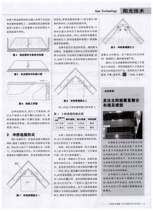
这种连 接形 式 , 因 为工 艺路 线短 ,所 以生 产效率大大高于 螺钉连 接形式 。 虽 然角部连 接力略小于 螺钉连 接 , 但连 接 的可 靠性非常高, 所 以组框的合格率仍 然是 10 0 % 。
图 8 冲挤原理 图之 二
综 上 所 述 ,3 种 连 接性 能 比 较见 表 1 。
表 1 3 种连接性畿比较
、 、 \连接 形 式
效果 \
螺钉连接
பைடு நூலகம்
生 产 效率 比较低
缩 口 连接 比较高
冲挤 连 接 最高
工 艺要 求 比较低
比较高
最高
3 冲挤连接形 式
缩 口 连接形式 , 在保证 连接可 靠性 的 同时 ,提高 了组框生产效率 ,但效率仍不够 高, 所 以有人设计 了冲挤连接方式 (见 图 7 )。 在 这 种 连 接 方式 中 , 冲 刀 对 型 材 的 内 表 面 进 行切 断和 变形 , 并迫使型腔 内的角
业 内相 关人 士 表 示 ,友 迭 在薄膜 领 域初期可 能仍是小规 模 生产的走 势 ,待技 术 有所 突破 后 , 再 进 行 布局 , 而 非如 同在 LCD 领 域 以 量取 胜 的 策 略模 式。
订 阅 本刊 请拨 :【o l o )8 8 6 8 1 8 4 3 转 8 0 2 7 5 3
4 5 。 接缝 变小 ,最 终 越 来越 严 密 。
新 的工 艺 总是 需 要 新材料和 新 工 艺 装
备与之相适 应 , 原型材端面和工 艺装备专
家设计 出相适 应 的产 品 , 使组 件生 产 变得
圜 简 单 、 可 靠 、 高 效 率 。
( 责 编 :王 碧 辉 )
企业 信息
图 6 组框工 序图
厦门友达光电(有兴趣可阅一阅)

厦门友达光电企业概况:友达光电原名为达碁科技,成立于1996年8月,2001年与联友光电合并后更名为友达光电,2006年再度与广辉电子合并。
友达经过与两家公司的合并,大尺寸面板市占率位居全球领先地位。
友达光电亦是全球第一家于纽约证交所(NYSE)股票公开上市之TFT-LCD设计、制造及研发公司。
公司自2008年起进军绿能产业,并于2010年将业务分为液晶显示器与太阳能二大事业体.全球每五片液晶面板就有一片来自友达光电。
全球领先的薄膜晶体管液晶显示器(TFT- LCD) 设计、研发及制造公司。
产品涵盖1.2寸至65寸TFT-LCD面板,是全球少数供应大、中、小完整尺寸产品线之厂商。
友达光电(厦门)有限公司位于厦门火炬高新区(翔安)产业区,现投入资本为4亿美金,现有员工7,281人(截止2011年01月),制造全产品线包括大中小尺寸的液晶面板模组,且产能随着客户端需求逐年增加。
我们的使命:成为世界顶尖的绿色方案企业我们的愿景:亮丽创新曼妙生活而其中的「绿叶」亦即代表「友达绿色承诺」。
此愿景将引领友达全员时时激发出亮丽的创新思考,为个人、社群及人类创造曼妙的生活型态,并透过落实「绿色承诺」爱护地球。
我们的核心价值观:以诚信为核心的三项核心价值观,分别为:「热情务本、追求卓越、关怀社会」及四项精神:「创新、纪律、效率、执行力」,这是所有友达人必须具备的工作态度与价值观,以及做事的方式和原则。
创新:勇于尝试创意思考,使企业再添新价值;持续改善,寻找最好的方法,务必尽善尽美。
开发不同事业、提供不同服务,让现有资源创造价值的改变。
有效利用资源,以创新的生产方式来满足市场需要。
纪律:自主管理,高度自律。
确实遵守组织约定。
主管以身作则,人人身体力行。
鸡婆心理,勇于纠正、辅导不守纪律者。
发挥团队精神,遵守团队纪律。
将守纪律的观念影响他人。
效率:嗅觉敏锐、反应敏捷、行动迅速、确实反馈。
最快速度完成任务。
最佳的成本考量。
- 1、下载文档前请自行甄别文档内容的完整性,平台不提供额外的编辑、内容补充、找答案等附加服务。
- 2、"仅部分预览"的文档,不可在线预览部分如存在完整性等问题,可反馈申请退款(可完整预览的文档不适用该条件!)。
- 3、如文档侵犯您的权益,请联系客服反馈,我们会尽快为您处理(人工客服工作时间:9:00-18:30)。
友达光电的TFT LCD、LCM 生产
友達光電目前擁有
4座3.5代廠,合計月產能13萬片(以及2萬片LTPS)
1座4代廠,月產能為6萬片
4座5代廠,月產能為31萬片
2座6代廠,月產能24萬片
1座7.5代廠,月產能7.5萬片
1座7.5 / 8.5代複合式廠房(hybrid fab),月產能4萬片
在具競爭力與最佳面板經濟切割的六代廠,友達光電擁有全球最大的產能。
此外,友達光電以台灣及大陸兩岸前後段TFT-LCD製程分工模式,有效降低生產成本。
友達光電搭配新增的TFT-LCD 前中段產能所需的後段模組線,已在中國的蘇州、松江與廈門設置模組廠進行生產,目前蘇州已進行大中小各種尺寸的面板模組生產,亦為全球第一家在中國同時具備大中小尺寸之模組廠,松江模組廠則以生產資訊顯示器產品為主,而廈門模組廠亦在2007年第二季量產。
為了積極拓展歐洲市場,友達在2008年於捷克設置模組廠,並已於2009年3月量產。
友達擁有全球先進的TFT-LCD廠房與設備,從3.5代到8.5代的各世代廠房保持產能與技術領先。
新竹科學工業園區:
L3A廠
3.5代廠
玻璃基板尺寸(mm): 610 x 720
量產時間: 1999 年12 月
月產能: 40,000 Sheets
已通過認證:ISO 14001、OHSAS 18001、
ISO 14064、ISO 9001、ISO/TS16949、
QC080000
路線圖
L3B廠
3.5代廠
玻璃基板尺寸(mm): 610 x 720
量產時間: 2000 年11 月
月產能: LTPS 20,000 Sheets
已通過認證:ISO 14001、OHSAS 18001、
ISO 14064、ISO 9001、ISO/TS16949、
QC080000
路線圖
L3C廠
3.5代廠
玻璃基板尺寸(mm): 600 x 720
量產時間: 1999 年7 月
月產能: 60,000 Sheets
已通過認證:ISO 14001、OHSAS 18001、
ISO 14064、ISO 9001、ISO/TS16949、
QC080000
路線圖
桃園華亞科學園區
L3D廠
3.5代廠
玻璃基板尺寸(mm): 620 x 750
量產時間: 2001 年12 月
月產能: a-Si 30,000 Sheets
已通過認證:ISO 14001、OHSAS 18001、
ISO 14064、ISO 9001、QC080000、
ISO/TS16949
路線圖
L5D廠
5代廠
玻璃基板尺寸(mm): 1100 x 1300
量產時間: 2003 年10 月
月產能: 70,000 Sheets
已通過認證:ISO 14001、OHSAS 18001、
ISO 14064、ISO 9001、QC080000、
ISO/TS16949
路線圖
龍潭渴望園區
L4A廠
4代廠
玻璃基板尺寸(mm): 680 x 880
量產時間: 2001 年 2 月
月產能: 60,000 Sheets
已通過認證:ISO 14001、OHSAS 18001、
ISO 14064、ISO 9001、ISO/TS16949、
QC080000
路線圖
L5A廠
5代廠
玻璃基板尺寸(mm): 1100 x 1250
量產時間: 2003 年 3 月
月產能: 50,000 Sheets
已通過認證:ISO 14001、OHSAS 18001、ISO
14064、ISO 9001、ISO/TS16949、QC080000
路線圖
L5B廠
5代廠
玻璃基板尺寸(mm): 1100 x 1300
量產時間: 2004 年 2 月
月產能: 70,000 Sheets
已通過認證:ISO 14001、OHSAS 18001、ISO
14064、ISO 9001、ISO/TS16949、QC080000
路線圖
龍潭科技園區
6代廠
玻璃基板尺寸(mm): 1500x 1850
量產時間: 2005 年8 月
月產能: 90,000 Sheets
已通過認證:ISO 14001、OHSAS 18001、ISO
14064、ISO 9001、QC080000、ISO/TS16949
路線圖
模組M02廠
量產時間: 2005 年7 月
已通過認證:ISO 14001、OHSAS 18001、
ISO 14064、ISO 9001、QC080000、
ISO/TS16949
路線圖
中部科學工業園區
L6A廠
6代廠
玻璃基板尺寸(mm): 1500 x 1850
量產時間: 2005 年第一季
月產能: 120,000 Sheets
已通過認證:ISO 14001、OHSAS 18001、
ISO 14064、ISO 9001、QC08000、
ISO/TS16949
路線圖
L5C廠
5代廠
玻璃基板尺寸(mm): 1100 x 1300
量產時間: 2005 年第三季
月產能: 120,000 Sheets
已通過認證:ISO 14001、OHSAS 18001、
ISO 14064、ISO 9001、QC080000、
ISO/TS16949
路線圖
L7廠
玻璃基板尺寸(mm): 1950 x 2250
量產時間: 2006 年第四季
月產能: 75,000 Sheets
已通過認證:ISO 14001、OHSAS 18001、
ISO 14064、ISO 9001、QC080000、
ISO/TS16949
路線圖
L8A廠
8.5代廠
玻璃基板尺寸(mm): 2200 x 2500
量產時間: 2009 年第二季
月產能: 40,000 Sheets
已通過認證:ISO 14001、OHSAS 18001、
ISO 14064、ISO 9001、QC080000、
ISO/TS16949、LEED
路線圖
中國
中國蘇州
模組S01, S02, S06廠
已通過認證:ISO 14001、OHSAS 18001、
ISO 14064、ISO 9001、ISO/TS16949、
QC080000
量產時間: 2002 年7 月
中國上海松江
模組S03廠
已通過認證:ISO 14001、OHSAS 18001、
ISO 14064、ISO 9001、ISO/TS16949、
QC080000
量產時間: 2004 年10 月
模組S11, S16廠
已通過認證:ISO 9001、ISO/TS16949、
QC080000
量產時間: 2007年4月
捷克布爾諾
模組E01廠
已通過認證:ISO 9001
量產時間: 2008 年 10 月。