正泰TC系列
TC系列产品

EIM400时隙分插设备
E1/RS-232/64Kbps
TC4110以太网桥
----E1/G.703接口的以太网桥
RJ017 ASIC
100MIPS处理能力 自主研制MJPEG图像压缩算法 G.723/728语音压缩算法 Sync/Async Communication Interface 适用于窄带通信处理
自主研制开发
性能价格比高
开放式设计,可根据用户实际需求定制/OEM 售后服务完善
TC4110应用之一
LAN
TC4110
E1/2M线路
TC4110
LAN
TC232应用之一
串口设备1,2,3,4
RS232/485 TC232
LAN/WAN
EIM400应用之一:点对点方式
BTS
E1/2M
E1/2M
欢迎光临 !
TC系列
网络通信产品
目录
第一章 亚奥数码概述
第二章
第三章
亚奥网络通信产品介绍
亚奥网络通信产品典型应用
第四章
质量保证及售后服务体系
第一章
公司概述
• • •
深圳市亚奥新实业有限公司简介 亚奥数码南京研究所简介 公司的多方面资质简介
北京北辰集团是以经营北京北城大型物业项目为主的国有大型企业集 团,为香港上市公司。主要物业项目有亚运村、五洲大酒店,世贸中 心等,本次北京申奥成功,北辰集团的工作重心将随之向奥运物业偏 移,从而带来新的一轮大发展。 深圳市亚奥新实业有限公司是北京北辰集团控股的高科技企业,主要 从事通信产品制造业,目前主要的产品有程控交换机,110、119调度 指挥系统,ProMonitor动力设备及环境远程集中监控系统, AnyShow网络视频监控系统以及无线网络通讯设备等。其上百种产品 的应用涵盖了邮电、电力、司法、金融、水利等国家枢纽部门,以‘ 优秀人才,优秀品质,优秀服务,服务于优秀民族’的创业宗旨为我 国的发展建设作出了应有的贡献。
正泰电器价格表

40A-50A 60A
6A-10A 15A-20A
30A 40A-50A
60A
DZ15-100/290 50A-100A DZ15-100/390 50A-100A
NM10-600/330 200A-600A
NM1-400S/3300 250A-400A NM1-400H/3300 250A-400A NM1-630S/3300 500A-630A
CJX1-系列交流接触器 CJX1-9/22 CJX1-12/22 CJX1-16/22 CJX1-22/22 CJX1-32/22 CJX1-45/22 CJX1-63/22 CJX1-75/22 CJX2-系列交流接触器 CJX2-0910 CJX2-0901 CJX2-1210 CJX2-1201 CJX2-1810 CJX2-1801 CJX2-2510 CJX2-2501 CJ12-系列交流接触器 CJ12-100/3 CJ12-150/3 CJ12-250/3 CJ20-系列交流接触器 CJ20-10 CJ20-16 CJ20-25 CJ20-40 CJ20-63 CJ40-系列交流接触器 CJ40-63 CJ40-100 CJ40-125 CJT1-系列交流接触器 CJT1-10 CJT1-20 CJT1-40 CJ19-系列切换电容接触器
DZ158-125 1P 80A DZ158-125 1P 100A(125A) DZ158-125 2P 63A DZ158-125 2P 80A DZ158-125 2P 100A(125A) NH2-100-系列隔离开关 NH2-100 1P 32A NH2-100 1P 63A NH2-100 1P 100A NH2-100 2P 32A NH2-100 2P 63A NH2-100 2P 100A NH4-125-系列隔离开关 NH4-125 1P 32A NH4-125 1P 63A NH4-125 1P 100(125)A NH4-125 2P 32A NH4-125 2P 63A NH4-125 2P 100(125)A DW15-系列万能式断路器 DW15-200A 热电磁式电动 DW15-400A 热电磁式电动 DW15-630A 热电磁式电动 DW15-1000A热电磁式电动 DW16-系列万能式断路器 DW16-200A 杠杆电磁式 DW16-400A 杠杆电磁式 DW16-630A 杠杆电磁式 DW17-系列万能式断路器 DW17-630A 电动固定垂直式 DW17-800A 电动固定垂直式 DW17-1000A 电动固定垂直式 DW17-1250 A电动固定垂直式 DW17-1600A 电动固定垂直式 DW17-2000A 电动固定垂直式 DW17-2500A 电动固定垂直式 DW17-3200A 电动固定垂直式
正泰TC端子
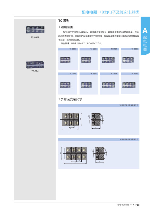
TC-1003
TC-1503
TC-1504
TC-6003
A
配 电 电 器
TC-604
TC-2003
TC-3003
TC-3004
TC-4004
2 外形及安装尺寸
TC系列三组外形及安装尺寸
D φF φG
L1 L
E
TC系列四组外形及安装尺寸
D φF φG
L1 L1
L
E
让 电 尽 其 所 能 >> A-718
序号
1 2 3 4 5 6 7 8 9 TC-1003 TC-1004 TC-1503 TC-1504 TC-2003 TC-2004 TC-3003 TC-3004 TC-4003 TC-4004 TC-6003 TC-6004
额定 电流 60A 60A 100A 100A 150A 150A 200A 200A 300A 300A 400A 400A 600A 600A
55
42
55
42
66
46
66
46
72
51
72
51
90
58
90
58
90
60
90
60
100.5
80
100.5
80
3 订货须知
3.1 订货时应注明产品的型号、额定电流、类别、数量。 3.2 常规的接线端子单独成条。 3.3 对于有其它特殊要求应注明。 3.4 订货示例:TC-603 5条
表示订货型号为TC,额定电流为60A,组数为3,总共数量为5条。
TC-6004
配电电器 电力电子及其它电器类
TC 系列
1 适用范围
TC适用于交流50Hz或60Hz、额定电压至600V、额定电流至600A的电路中,作导 线间的连接之用。本系列产品采用螺钉压接连接,导线端头需压接接线鼻后才能与接线端 子连接。采用螺钉安装。
正泰产品系列类别剖析
断相与欠压.相序保护继电器
系列断相与相序保护继电器
NJYBk XJ3
小型电磁继电器
通用型小型大功率电磁继电器
NJQX-lk JQX-10F. JTX. JMK
无氧化零飞弧电磁继电器
NJX-13FW
超小型大功率电磯继电器
NJQC-3FW. JQC-3F
NPS
系列单相应急电源
NEPS
系列三相应急电源
NEPS
电流互感器
型电流互感器
NLH1-0.66.BH-0.66IxBH(SDH)-0.66II、BH・0・66 III . RCT、LQG・0・66、LQZJ1・O・66、LMZ(J)l-0.66. LMZ3-0.66. LMZ1-0.5 LMZJ1-0J > LM-0.5xLMZW1-0.5. LMZW2-0.5
IIE40
户外隔离开关
型户外高压隔离开关
GW9. HGW9-12
系列低压户外烙断器式隔离开关
JDW
负荷开关
系列负荷开关
HH3、
开启式负荷开关
HK2
隔离开关
HK18
转换开关
系列自动转换开关电器
NZ1B. NZ7
自动转换开关电器
NZ1BR・63/(NB1・63H)、NZ1BR-60ADZ47).
负载型开关
系列中间继电器
JZ7
模数化继电器(监控与保护)
液位继电器
NJBl-YWx
继电器(相序.缺相、三相不平衡保护)
NJB1-X
继电器(相序.缺相保护〉
NJB1-X1
单相电压继电器
NJB1-Y
正泰集团C安全认证证书一览表
DZ20Y ,J-630 3P 4P DZ20Y ,J-400 3P 4P
DZ20C-400 3P NM1-63S. H 3P 4P
DZ5-50 3P DZ5-20 3P NRE8-40 DZ20C-250 3P DZ20Y.J.G-225/3P DZ20J-225/4P
正泰集团3C安全认证证书一览表 第6页 型号规格 DZ20C-160 3P DZ20Y. J.G-100/3P DZ20J-100/4P DW15-4000 DW15-2500 HD11-600 3P HD11-200 3P NRC8-40.31.22 HD11-400 RT14-32 RT14-20 RT14-63 HDLRS-200 HDLRS-150 HDLRS-100 HDLRT0-600 HDLRT0-400
正泰集团3C安全认证证书一览表 第7页 型号规格 HDLRT0-200 HDLRT0-100 RT28-63 RT28-32
99 A0009444 100 A0009445 101 A0009446 102 A0009447 103 A0009448 104 A0009449 105 A0009450 106 A0009451 107 A0009452 108 A0009453 109 A0009454 110 A0009455
70 A0009414 71 A0009415 72 A0009416 73 A0009416 74 A0009418 75 A0009419 76 A0009420 77 A0009421 78 A0009422
序号 序 编
79 A0009423 80 A0009424 81 A0009425 82 A0009426 83 A0009427 84 A0009427 85 A0009429 86 A0009430 87 A0009432 88 A0009433 89 A0009434 90 A0009435 91 A0009436 92 A0009437 93 A0009438 94 A0009439
TC系列 智能温控表使用说明书

智能温控表使用说明书本说明书对温控表设置、配线及各部分名称等进行说明,使用本产品前,请认真阅读本说明书,在理解内容的基础上正确使用。
并请妥善保存,以便需要时参考。
⊙支持多种热电偶、热电阻信号类型⊙采用模糊PID 控制算法,且自整定无过冲⊙多种控制方式可选,具体请参照OT 参数⊙RUN/STOP,运行/停止功能一键切换特点KKTCC02A-A/1-202009032、隔离模式框图:固态继电器输出绝缘电阻静电放电脉冲群抗扰度浪涌抗扰度电压暂降及短时中断抗扰度隔离耐压DC 24V 脉冲电平,带载<30mA 输入、输出、电源对机壳>20MΩIEC/EN61000-4-2 Contact ±4KV /Air ±8KV perf.Criteria B IEC/EN61000-4-4 ±2KV perf.Criteria B IEC/EN61000-4-5 ±2KV perf.Criteria BIEC/EN61000-4-29 0%~70% perf.Criteria B信号输入与输出及电源1500VAC 1min,60V 以下低压电路之间DC500V,1min 整机重量约 400g机壳材质面贴材质停电数据保护面板防护等级安全标准外壳与面板基架PC/ABS (难燃度UL94V-0)PET(F150/F200)10年,可写数据次数100万次IP65(IEC60529)IEC61010-1 过电压分类Ⅱ,污染等级2,等级Ⅱ(加强绝缘)3、测量信号参数表:1、电气参数表:采样速度2次每秒供电电源继电器容量AC 250V /3A 额定负载寿命大于10万次AC/DC 100~240V (85-265V)三、主要技术参数二、常规型号说明一、仪表型号周围环境条件整机功耗存贮环境< 6VA室内使用,温度:0~50℃ 无结露,湿度:<85%RH,海拔小于2000m -10~60℃,无结露SSR与继电器输出型 号控制输出功能1报警接点TC-□-M1□:外形尺寸可选E:版本1:一路报警输出 2:两路报警 空: 无报警功能4: 48W*48H*100L 6:48W*96H*100L 7:72W*72H*100L 8:96W*48H*100L 9:96W*96H*100LTC系列温控表注意:选择加热冷却控制方式时,如还需报警功能,请选择带两路报警的型号。
常用正泰低压件A
额定电流 1~1.6A 1.25~2A 1.6~2.5A 2~3.2A 2.5~4A 3.2~5A 4~6.3A 5~8A 6.3~10A 8~12.5A 10~16A 12.5~20A 16~25A 20~32A 25~40A 32~45A 40~57A 50~63A 55~80A 63~90A 80~110A 90~120A 110~135A 120~150A 135~160A
NM1-1250H/3300 700~1250A 正泰小型断路器1P/2P 型号 DZ47-60/1P-C1A DZ47-60/1P-C2A DZ47-60/1P-C3A DZ47-60/1P-C4A DZ47-60/1P-C5A DZ47-60/1P-C10A DZ47-60/1P-C15A DZ47-60/1P-C20A DZ47-60/1P-C25A DZ47-60/1P-C32A DZ47-60/1P-C40A DZ47-60/1P-C50A DZ47-60/1P-C60A DZ47-60/2P-C1A DZ47-60/2P-C2A DZ47-60/2P-C3A DZ47-60/2P-C4A DZ47-60/2P-C5A DZ47-60/2P-C10A DZ47-60/2P-C15A DZ47-60/2P-C20A DZ47-60/2P-C25A DZ47-60/2P-C32A DZ47-60/2P-C40A DZ47-60/2P-C50A 额定电流 1A 2A 3A 4A 5A 10A 15A 20A 25A 32A 40 50A 60A 1A 2A 3A 4A 5A 10A 15A 20A 25A 32A 40 50A
NR4系列热继电器(独立式)
序号 1 2 3 4 5 6 7 8 9 10 11 12 13 14 15 16 17 18 19 20 21 22 23 24 25 26 序号 1 2 3 4 5 6 7 8 9 10 11 12 13 14 15 16
正泰开关 CAT6202-D 使用说明书
To learn more about onsemi™, please visit our website atON SemiconductorIs NowCAT6202LDO Regulator - Adjustable CMOS500 mA, 13 VDescriptionThe CA T6202 is a 13 V rated 500 mA CMOS low dropout regulatorvoltage at V occur.Features•••Input V •••••V OUT •Soft −••±•±•Thermal Protection •8 Pad TDFN Package•These Devices are Pb −Free, Halogen Free/BFR Free and are RoHS CompliantSee detailed ordering and shipping information in the package dimensions section on page 10 of this data sheet.Figure 1. CAT6202 Typical Applicationm FV INV OUTTable 1. PIN FUNCTION DESCRIPTIONPin No.Pin Name Description1VIN Supply voltage input2FLT Fault indicator (active low)3EN Enable input (active high)4BYP A capacitor between BYP and GND controls the regulator’s turn−on speed and improves PSRR5GND Ground reference6ILIM Current limit control pin7VADJ Output voltage adjustment8VOUT LDO Output VoltageTable 2. ABSOLUTE MAXIMUM RATINGSRating Value UnitV IN, V OUT0 to 16VAll other pins−0.3 to +6.0V Junction Temperature, T J+150_C Power Dissipation, P D Internally Limited (Note 1)mW Storage Temperature Range, T S−65 to +150_C Lead Temperature (soldering, 5 sec.)260_C ESD Rating (Human Body Model)1000V ESD Rating (Machine Model)350V Stresses exceeding those listed in the Maximum Ratings table may damage the device. If any of these limits are exceeded, device functionality should not be assumed, damage may occur and reliability may be affected.1.The maximum allowable power dissipation at any T A (ambient temperature) is P Dmax = (T Jmax – T A) / θJA. Exceeding the maximum allowablepower dissipation will result in excessive die temperature, and the regulator will go into thermal shutdown.Table 3. RECOMMENDED OPERATING CONDITIONS (Note 2)Parameter Range UnitV IN, V OUT 3.3 to 13.5VAll other pins0 to 6.0V Junction Temperature Range, T J−40 to +125_C Package Thermal Resistance (SOIC), θJA235_C/W Package Thermal Resistance (TDFN), θJA92_C/W Functional operation above the stresses listed in the Recommended Operating Ranges is not implied. Extended exposure to stresses beyond the Recommended Operating Ranges limits may affect device reliability.2.The device is not guaranteed to work outside its operating rating.Pin FunctionVIN is the supply pin for both the LDO’s operation and the load the LDO is driving. It is recommended that a 1 m F ceramic bypass capacitor be placed between the V IN pin and ground in close proximity to the device. When using longer connections to the power supply, C IN value can be increased without limit. The operating input voltage range is from 3.3 V to 13 V .FLT is an active low open −drain output indicating one of 3fault conditions:1.Input under −voltage: V IN is below the intendedand/or the ground plane of the PCB. Connection to the ground plane enhances thermal conductivity drawing heat out of the package and into the surrounding PCB.ILIM stands for Current Limit and is the control input for setting the point at which the current limit is invoked. I LIMis defined as the current at which V OUT is still within 80%of its nominal value and should not be confused with I SC , the short circuit current, measured at V OUT = 0 V , which is typically 100 mA greater than I LIM .A resistor R EXT placed between I LIM and GND selects the trip current according to a formula:I LIMIT +I LIMIT0)Current_Limit_Factor(CLF)R EXT(eq. 1)I LIM0 is the built −in minimum current limit (typically 150 mA), and CLF is a numerical value (typical 30,000V olts) which relates the allowable load current to a (eq. 2)(eq. 3)m F ceramic (eq. 4)−temp VOUT is protected against the application of voltages greater than VIN. For example, in automotive applications,if CAT6202 is powering a remote load and damage occurs to a wiring harness shorting a powered line, Battery + for instance, to VOUT, CAT6202 will not be damaged by this higher voltage being applied to VOUT.Table 4. ELECTRICAL CHARACTERISTICS(V IN = V OUT + 1 V, V EN = High, I OUT = 1 mA, C IN = 1 m F, C OUT = 2.2 m F, R EXT= 47 k W, ambient temperature of 25°C (over recommended operating conditions unless specified otherwise). Bold numbers apply for the entire junction temperature range.)Symbol Parameter Conditions Min Typ Max Unit V IN Input Voltage 3.313.5V V OUT Output Voltage V ADJ12.5V ADJ ADJ Voltage 1.238 1.250 1.262VI ADJ ADJ Input Current0.5 2.0m ATC OUT Output Voltage Temp. Coefficient40ppm/°C V R−LINE Line Regulation V OUT + 1.0 < V IN < 13 V−0.2±0.1+0.2%/V−0.4+0.4V R−LOAD Load Regulation I OUT = 1 mA to 500 mA1 2.5% V DROP Dropout Voltage (Note 3)I OUT = 500 mA250350mVI GND Ground Current I OUT = 0 mA100150m AI OUT = 500 mA160300I GND−SD Shutdown Ground Current V EN < 0.4 V2m APSRR Power Supply Rejection Ratio f = 1 kHz, C BYP = 10 nF62dBf = 20 kHz, C BYP = 10 nF52T ON Turn−On Time C BYP = 10 nF700m sI SC Output short circuit current V OUT < 0.8 V7008001000mAI LIM Output current limit V OUT = 0.8 V OUT (1 mA)600650800mACLF Current Limit Factor V OUT < 0.8 V243036KV t FD Fault Delay 1.536msV IN−UVLO Under voltage lockout threshold 3.1V ESR R OUT equivalent series resistance5500m W ENABLE INPUTV HI Logic High Level V IN = 3.3 to 13 V2V V LO Logic Low Level V IN = 3.3 to 13 V0.4VI EN Enable Input Current V EN = 0.4 V0.151m AV EN = V IN35THERMAL PROTECTIONT SD Thermal Shutdown140°C T HYS Thermal Hysteresis10°C3.Dropout voltage is defined as the input−to−output differential at which the output voltage drops 2% below its nominal value. During test, theinput voltage stays always above the minimum 3.3 V. The given values are for V OUT = 7.5 V.Product parametric performance is indicated in the Electrical Characteristics for the listed test conditions, unless otherwise noted. Product performance may not be indicated by the Electrical Characteristics if operated under different conditions.Figure 7. Ground Current vs. Load Current Figure 8. Ground Current vs. TemperatureOUTPUT LOAD CURRENT (mA)TEMPERATURE (°C)O U T P U T V O L T A G E (V )O U T P U T V O L T A G E (V )G R O U N D C U R R E N T (m A )Figure 13. Output Voltage vs. Load CurrentFigure 14. Output Current (Sink) vs. OutputVoltageOUTPUT CURRENT (mA)OUTPUT VOLTAGE (V)S H O R T −C I R C U I T C U R R E N T (m A )E N A B L E T H R E S H O L D V O L T A G E (V )O U T P U T V O L T A G E (V )TYPICAL CHARACTERISTICS (shown for 7.5 V output)(V IN = 8.5 V, R 1 = 5.1 k W , R 2 = 1 k W , C IN = 1 m F, C OUT = 2.2 m F, C BYP = 10 nF, R EXT = 47 k W ,T A = 25°C unless otherwise specified. All transient characteristics are generated using the evaluation board CAT6202EVAL1.)Figure 15. Enable Turn −On (No Load)Figure 16. Enable Turn −On (15 W Load)Figure 17. Enable Operation (No Load)Figure 18. Enable Operation (15 W Load)Figure 19. Load Transient Response(1 mA to 500 mA)Figure 20. Fault Operation (VIN = 7 V and 15 W Load)PACKAGE DIMENSIONSTDFN8, 2x3CASE 511AK−01ISSUE A(2) Complies with JEDEC MO-229.CAT6202 Table 5. ORDERING INFORMATIONDevice Order NumberSpecificDevice Marking Package TypeLeadFinish Shipping†CAT6202VP2−GT3HXC TDFN−8NiPdAu Tape & Reel, 3,000 Units / Reel†For information on tape and reel specifications, including part orientation and tape sizes, please refer to our Tape and Reel Packaging Specifications Brochure, BRD8011/D.and are registered trademarks of Semiconductor Components Industries, LLC (SCILLC). SCILLC owns the rights to a number of patents, trademarks, copyrights, trade secrets, and other intellectual property. A listing of SCILLC’s product/patent coverage may be accessed at /site/pdf/Patentreserves the right to make changes without further notice to any products herein. SCILLC makes no warranty, representation or guarantee regarding the suitability of its products for any particular purpose, nor does SCILLC assume any liability arising out of the application or use of any product or circuit, and specifically disclaims any and all liability, including without limitation special, consequential or incidental damages. “Typical” parameters which may be provided in SCILLC data sheets and/or specifications can and do vary in different applications and actual performance may vary over time. All operating parameters, including “Typicals” must be validated for each customer application by customer’s technical experts. SCILLC does not convey any license under its patent rights nor the rights of others. SCILLC products are not designed, intended, or authorized for use as components in systems intended for surgical implant into the body, or other applications intended to support or sustain life, or for any other application in which the failure of the SCILLC product could create a situation where personal injury or death may occur. Should Buyer purchase or use SCILLC products for any such unintended or unauthorized application, Buyer shall indemnify and hold SCILLC and its officers, employees, subsidiaries, affiliates, and distributors harmless against all claims, costs, damages, and expenses, and reasonable attorney fees arising out of, directly or indirectly, any claim of personal injury or death associated with such unintended or unauthorized use, even if such claim alleges that SCILLC was negligent regarding the design or manufacture of the part. SCILLC is an Equal Opportunity/Affirmative Action Employer. This literature is subject to all applicable copyright laws and is not for resale in any manner.PUBLICATION ORDERING INFORMATIONLITERATURE FULFILLMENT:Literature Distribution Center for ON Semiconductor.O. Box 5163, Denver, Colorado 80217 USA2175 or 800−2176 or 800−344:*******************。
CHINT CN C33 NB8 系列 小型断路器说明书
400-817-浙江办事处(浙江省、福建省)地址:浙江省乐清市北白象镇硐桥村华山路 正泰大桥物流园区江苏办事处(江苏省、安徽省)地址:江苏省南京市建邺区河西大街66号 徐矿明星商务中心11楼北山东办事处(山东省)地址:山东省济南市市中区二环南路2666号 鲁能国际中心2403室河南办事处(河南省、山西省)地址:河南省郑州市花园路 信息大厦1707室四川办事处(四川省、重庆市)地址:四川省成都市武候区航空路6号 丰德国际B1-3AF 湖南办事处(湖南省、江西省)地址:湖南省长沙市万家丽中路一段 旺德府国际大厦1406-1407辽宁办事处(辽宁省、吉林省、内蒙古东部)地址:辽宁省沈阳市和平区南京南街197号 (长白地区)汇锦金融中心801室湖北办事处(湖北省)地址:湖北省武汉市江汉区后襄河北路 海马公园1栋1201-1205云南办事处(云南省、贵州省)地址:贵州省贵阳市观山湖区 黔桂国际商务中心1504号新疆办事处(新疆维吾尔自治区)地址:新疆乌鲁木齐市天山区光明路 时代广场A 座7G 室广西办事处(广西壮族自治区)地址:广西南宁市青秀区东葛路118号 青秀万达广场西2栋2018号黑龙江办事处(黑龙江省)地址:黑龙江省哈尔滨市南岗区中兴大街万达广场写字楼B1栋2310室在全球能源发展面临资源紧张、环境污染、气候变化三大难题的背景下,能源格局优化成必然趋势。
正泰积极推进“一云两网”战略布局,持续分阶段推进大数据、物联网、人工智能与制造业的深度融合,着力打造平台型企业,引领行业发展新风向。
正泰云正泰云是智慧科技与数据应用的载体,连接企业内部制造与经营管理数据,实现企业对内与对外的数字化应用与服务。
正泰能源物联网 EIoT 正泰能源物联网是以用户为中心的多能互补的智慧能源体系,为政府、工商业及终端用户提供一揽子能源解决方案,业务涵盖智慧能效、智慧电力、智能家居、智慧新能源等。
正泰工业物联网 IIoT 正泰工业物联网是以企业数字化转型为核心的智能制造体系,构建形成灵活、高效、智慧的工业体系,业务涵盖智能制造、智慧工业、智慧水务、智慧供热等。
如何看懂正泰空气开关型号
如何看懂正泰空气开关型号只要电路中的电流超过额定电流,空气开关就会自动断开从而对电路起到一定的保护作用,也让我们的用电安全更有保障。
正泰空气开关是一个知名度比较高的开关品牌,下面小编将为大家解读正泰空气开关型号。
空气开关的规格型号有很多,比较常用的就是DZ系列的空气开关。
常见的几种空气开关的规格型号有C16、C40、C32、C80、C60、C100、C120等几种,也是目前比较常用的几种空气开关规格型号。
此外,除了这种家居装置的空气开关规格型号之外,还有用于工业上的空气开关,比较常用的就是DZ和DW系列,其规格型号有32A、80A、100A、160A、250A、400A、800A、1000A等几种,也许还有更高的空气开关型号。
以上是几种比较常用的家装空气开关规格型号,也有工业上所用的空气开关规格型号,这样数字类型的规格也许很多人都看不懂也或者不是很了解。
其实家用的空气开关规格型号里面的大写字母C表示脱扣电流,数字则表示电流的大小,这些规格型号所适用的范围是不同的,比如家里安装的热水器是7000W-8500W左右,则采用的空气开关规格型号就需要用脱扣电流为40安的电流,即C40。
正泰空气开关C型和D型的区别是看型号的最后一位,比如DZ15LE-100/4901,指的是DZ15漏电,100A,三相四线,最后一位1,表示照明,电机用途是4902,当然了,市面上除了DZ47系列以外,其他的断路器都是4901,也就是照明的有备货,用来带电机也不怕的。
因为现在的电工,在选型的时候都相应的放大了电流等级,除非是50KW的电机,选用了100A的断路器,这样,哪怕是电机用途的,都会烧掉。
因为现在的国产断路器,实际过电流达不到100%的。
C型空气开关的脱扣电流一般是额定电流的5倍左右适合照明用,可保护线路,特性适用于感性负载和高感照明回路;D型空气开关的脱扣电流一般是额定电流的10倍左右适合工业用,电机的启动电流很大,不至于在启动时跳闸,特性适用于高感负载和较大冲击电流的配电系统。