Ti(德州仪器)-芯片手册-cd4030b
德州仪器(TI) BQ34Z100宽量程电量监测计说明书

BQ34Z100 采用 Impedance Track™ 技术的宽量程电量监测计1 特性•支持锂离子和磷酸铁锂化学物质•对电压为 3V 至 65V 的电池使用已获得专利的 Impedance Track™技术估算容量–老化补偿–自放电补偿•支持超过 65Ah 的电池容量•支持高于 32A 的充放电电流•外部负温度系数 (NTC) 热敏电阻支持•支持与主机系统的两线制 I2C 和 HDQ 单线制通信接口•SHA-1/HMAC 认证•一个或者四个 LED 直接显示控制•五个 LED 和通过端口扩展器的更多显示•节能模式(典型电池组运行范围条件)–正常工作:< 140µA 平均电流–睡眠:< 64µA 平均电流–全睡眠:< 19µA 平均电流•封装:14 引脚 TSSOP 2 应用•轻型电动车辆•医疗仪器•移动无线电•电动工具•不间断电源 (UPS)3 说明德州仪器 (TI) BQ34Z100 是独立于电池串联配置工作的电量监测计解决方案,支持各种锂离子和磷酸铁锂电池化学物质。
通过外部电压转换电路可支持 3V 至 65V 的电池,此电路可通过自动控制来降低系统功耗。
BQ34Z100 器件提供多个接口选项,其中包括一个 I2C 从接口、一个 HDQ 从接口、一个或四个直接 LED 接口以及一个警报输出引脚。
此外,BQ34Z100 还支持外部端口扩展器,连接四个以上的 LED。
(1)如需了解所有可用封装,请参阅数据表末尾的可订购产品附录。
简化版原理图Table of Contents1 特性...................................................................................12 应用...................................................................................13 说明...................................................................................14 Revision History ..............................................................25 Pin Configuration and Functions ...................................36 Specifications ..................................................................46.1 Absolute Maximum Ratings........................................46.2 ESD Ratings...............................................................46.3 Recommended Operating Conditions.........................46.4 Thermal Information....................................................56.5 Electrical Characteristics: Power-On Reset................56.6 Electrical Characteristics: LDO Regulator...................56.7 Electrical Characteristics: Internal TemperatureSensor Characteristics..................................................56.8 Electrical Characteristics: Low-FrequencyOscillator.......................................................................66.9 Electrical Characteristics: High-FrequencyOscillator.......................................................................66.10 Electrical Characteristics: Integrating ADC(Coulomb Counter) Characteristics...............................66.11 Electrical Characteristics: ADC (Temperatureand Cell Measurement) Characteristics........................66.12 Electrical Characteristics: Data Flash MemoryCharacteristics (7)6.13 Timing Requirements: HDQ Communication............76.14 Timing Requirements: I 2C-Compatible Interface......86.15 Typical Characteristics..............................................97 Detailed Description ......................................................107.1 Overview...................................................................107.2 Feature Description...................................................117.3 Device Functional Modes..........................................398 Application and Implementation ..................................408.1 Typical Applications..................................................409 Power Supply Recommendations ................................4910 Layout ...........................................................................5010.1 Layout Guidelines...................................................5010.2 Layout Example......................................................5011 Device and Documentation Support ..........................5311.1 Documentation Support..........................................5311.2 接收文档更新通知...................................................5311.3 支持资源..................................................................5311.4 Trademarks.............................................................5311.5 Electrostatic Discharge Caution..............................5311.6 术语表.....................................................................5312 Mechanical, Packaging, and OrderableInformation (53)4 Revision History注:以前版本的页码可能与当前版本的页码不同Changes from Revision B (December 2012) to Revision C (May 2021)Page•根据更新的德州仪器 (TI) 标准更改了文档格式并通篇更新了 SRP 和 SRN 引脚................................................1•Changed Ground System ................................................................................................................................50•Changed Board Offset Considerations ............................................................................................................51Changes from Revision A (September 2012) to Revision B (December 2012)Page•Changed Absolute Maximum Ratings ...............................................................................................................4•Changed 节 6.3 ..................................................................................................................................................4•Changed 节 7.2.15.3 ........................................................................................................................................39•Changed SLEEP Mode ....................................................................................................................................39•Changed FULL SLEEP Mode ..........................................................................................................................39•Changed STEP 3 (44)BQ34Z100ZHCS926C – MAY 2012 – REVISED MAY 20215 Pin Configuration and FunctionsP2P3/SDA VEN P4/SCL P1P5/HDQ BAT P6/TS CE SRN REGIN SRP REG25VSSBQ34Z100ZHCS926C – MAY 2012 – REVISED MAY 2021BQ34Z100ZHCS926C – MAY 2012 – REVISED MAY 6 Specifications6.1 Absolute Maximum Ratings(1)(1)Stresses beyond those listed under absolute maximum ratings may cause permanent damage to the device. These are stress ratingsonly, and functional operation of the device at these or any other conditions beyond those indicated under recommended operating conditions is not implied. Exposure to absolute–maximum–rated conditions for extended periods may affect device reliability.6.2 ESD Ratings(1)JEDEC document JEP155 states that 500-V HBM allows safe manufacturing with a standard ESD control process.(2)JEDEC document JEP157 states that 250-V CDM allows safe manufacturing with a standard ESD control process.6.3 Recommended Operating Conditions6.3 Recommended Operating Conditions (continued)6.4 Thermal Information(1)For more information about traditional and new thermal metrics, see the Semiconductor and IC Package Thermal Metrics Application Report , SPRA953.6.5 Electrical Characteristics: Power-On Reset6.6 Electrical Characteristics: LDO Regulator(1)(1)LDO output current, I OUT , is the sum of internal and external load currents.(2)Specified by design. Not production tested.6.7 Electrical Characteristics: Internal Temperature Sensor CharacteristicsBQ34Z100ZHCS926C – MAY 2012 – REVISED MAY 2021BQ34Z100ZHCS926C – MAY 2012 – REVISED MAY 6.8 Electrical Characteristics: Low-Frequency Oscillator(1)The frequency drift is included and measured from the trimmed frequency at VCC = 2.5 V, T A = 25°C.(2)The frequency error is measured from 32.768 kHz.(3)The startup time is defined as the time it takes for the oscillator output frequency to be ±3%.6.9 Electrical Characteristics: High-Frequency Oscillator(1)The frequency error is measured from 2.097 MHz.(2)The startup time is defined as the time it takes for the oscillator output frequency to be ±3%.6.10 Electrical Characteristics: Integrating ADC (Coulomb Counter) Characteristics(1)Specified by design. Not tested in production.(2)Full-scale reference6.11 Electrical Characteristics: ADC (Temperature and Cell Measurement) Characteristics6.11 Electrical Characteristics: ADC (Temperature and Cell Measurement) Characteristics (continued)(1)Specified by design. Not tested in production.6.12 Electrical Characteristics: Data Flash Memory Characteristics(1)Specified by design. Not tested in production.6.13 Timing Requirements: HDQ CommunicationT A = –40°C to 85°C, C REG = 1.0 μF, 2.45 V < V REGIN = V BAT < 5.5 V; typical values at T A = 25°C and V REGIN = V BAT = 3.6 VBQ34Z100ZHCS926C – MAY 2012 – REVISED MAY 2021(a)Break and Break Recovery(c)Host Transmitted Bit(d)Gauge Transmitted Bit(b)HDQ line rise time图 6-1. Timing Diagrams6.14 Timing Requirements: I2C-Compatible InterfaceT A = –40°C to 85°C, C REG = 0.47 μF, 2.45 V < V REGIN = V BAT < 5.5 V; typical values at T A = 25°C and V REGIN = V BAT = 3.6t SU(STA)SCLSDAt w(H)tw(L)t f tr t(BUF)t rt d(STA)REPEATEDSTARTt h(DAT)t su(DAT)t f t su(STOP)STOP START图 6-2. I2C-Compatible Interface Timing DiagramsBQ34Z100ZHCS926C – MAY 2012 – REVISED MAY 6.15 Typical CharacteristicsBQ34Z100ZHCS926C – MAY 2012 – REVISED MAY 2021BQ34Z100ZHCS926C – MAY 2012 – REVISED MAY 7 Detailed Description7.1 OverviewThe BQ34Z100 device accurately predicts the battery capacity and other operational characteristics of a single cell or multiple rechargeable cell blocks, which are voltage balanced when resting. The device supports various Li-ion and LiFePO4 chemistries, and can be interrogated by a host processor to provide cell information, such as remaining capacity, full charge capacity, and average current.Information is accessed through a series of commands called Standard Data Commands (see 节7.2.1.1). Further capabilities are provided by the additional Extended Data Commands set (see 节 7.2.2). Both sets of commands, indicated by the general format Command(), are used to read and write information contained within the BQ34Z100 device’s control and status registers, as well as its data flash locations. Commands are sent from host to gauge using the BQ34Z100 serial communications engines, HDQ and I2C, and can be executed during application development, pack manufacture, or end-equipment operation.Cell information is stored in the BQ34Z100 in non-volatile flash memory. Many of these data flash locations are accessible during application development and pack manufacture. They cannot, generally, be accessed directly during end-equipment operation. Access to these locations is achieved by using the BQ34Z100 device’s companion evaluation software, through individual commands, or through a sequence of data-flash-access commands. To access a desired data flash location, the correct data flash subclass and offset must be known. The BQ34Z100 provides 32 bytes of user-programmable data flash memory. This data space is accessed through a data flash interface. For specifics on accessing the data flash, refer to 节 7.2.3.The key to the BQ34Z100 device’s high-accuracy gas gauging prediction is Texas Instrument’s proprietary Impedance Track algorithm. This algorithm uses voltage measurements, characteristics, and properties to create state-of-charge predictions that can achieve accuracy with as little as 1% error across a wide variety of operating conditions.The BQ34Z100 measures charge/discharge activity by monitoring the voltage across a small-value series sense resistor connected in the low side of the battery circuit. When an application’s load is applied, cell impedance is measured by comparing its Open Circuit Voltage (OCV) with its measured voltage under loading conditions.The BQ34Z100 can use an NTC thermistor (default is Semitec 103AT or Mitsubishi BN35-3H103FB-50) for temperature measurement, or can also be configured to use its internal temperature sensor. The BQ34Z100 uses temperature to monitor the battery-pack environment, which is used for fuel gauging and cell protection functionality.To minimize power consumption, the BQ34Z100 has three power modes: NORMAL, SLEEP, and FULL SLEEP. The BQ34Z100 passes automatically between these modes, depending upon the occurrence of specific events. Multiple modes are available for configuring from one to 16 LEDs as an indicator of remaining state of charge. More than four LEDs require the use of one or two inexpensive SN74HC164 shift register expanders.A SHA-1/HMAC-based battery pack authentication feature is also implemented on the BQ34Z100. When the IC is in UNSEALED mode, authentication keys can be (re)assigned. A scratch pad area is used to receive challenge information from a host and to export SHA-1/HMAC encrypted responses. See 节 7.2.14.1 for further details.备注Formatting conventions in this document:Commands: italics with parentheses and no breaking spaces; for example, RemainingCapacity().Data Flash: italics, bold, and breaking spaces; for example, Design Capacity.Register Bits and Flags: brackets only; for example, [TDA] DataFlash Bits: italic and bold; for example, [LED1]Modes and states: ALL CAPITALS; for example, UNSEALED mode.7.2 Feature Description7.2.1 Data Commands7.2.1.1 Standard Data CommandsThe BQ34Z100 uses a series of 2-byte standard commands to enable host reading and writing of battery information. Each standard command has an associated command-code pair, as indicated in 表 7-1. Because each command consists of two bytes of data, two consecutive HDQ/I2C transmissions must be executed to initiate the command function and to read or write the corresponding two bytes of data. Standard commands are accessible in NORMAL operation. Also, two block commands are available to read Manufacturer Name and Device Chemistry. Read/Write permissions depend on the active access mode.7.2.1.2 Control(): 0x00/0x01Issuing a Control() command requires a subsequent two-byte subcommand. These additional bytes specify the particular control function desired. The Control()command allows the host to control specific features of the BQ34Z100 during normal operation, and additional features when the BQ34Z100 is in different access modes, as described in 表 7-2.7.2.1.2.1 CONTROL_STATUS: 0x0000Instructs the fuel gauge to return status information to Control addresses 0x00/0x01. The status word includes the following information.Legend: RSVD = ReservedFAS:Status bit that indicates the BQ34Z100 is in FULL ACCESS SEALED state. Active when set.SS:Status bit that indicates the BQ34Z100 is in the SEALED state. Active when set.CALMODE:Status bit that indicates the BQ34Z100 calibration function is active. True when set.Default is 0.CCA:Status bit that indicates the BQ34Z100 Coulomb Counter Calibration routine is active. Active when set.BCA:Status bit that indicates the BQ34Z100 Board Calibration routine is active. Active when set.CSV:Status bit that indicates a valid data flash checksum has been generated. Active when set.FULLSLEEP:Status bit that indicates the BQ34Z100 is in FULL SLEEP mode. True when set. The state can only be detected by monitoring the power used by the BQ34Z100 because any communication will automatically clear it.SLEEP:Status bit that indicates the BQ34Z100 is in SLEEP mode. True when set.LDMD:Status bit that indicates the BQ34Z100 Impedance Track algorithm using constant-power mode. True when set.Default is 0 (CONSTANT CURRENT mode).RUP_DIS:Status bit that indicates the BQ34Z100 Ra table updates are disabled. True when set.VOK:Status bit that indicates cell voltages are OK for Qmax updates. True when set.QEN:Status bit that indicates the BQ34Z100 Qmax updates are enabled. True when set.7.2.1.2.2 DEVICE TYPE: 0x0001Instructs the fuel gauge to return the device type to addresses 0x00/0x01.7.2.1.2.3 FW_VERSION: 0x0002Instructs the fuel gauge to return the firmware version to addresses 0x00/0x01.7.2.1.2.4 HW_VERSION: 0x0003Instructs the fuel gauge to return the hardware version to addresses 0x00/0x01.7.2.1.2.5 RESET_DATA: 0x0005Instructs the fuel gauge to return the number of resets performed to addresses 0x00/0x01.7.2.1.2.6 PREV_MACWRITE: 0x0007Instructs the fuel gauge to return the previous command written to addresses 0x00/0x01. The value returned is limited to less than 0x0020.7.2.1.2.7 CHEM ID: 0x0008Instructs the fuel gauge to return the chemical identifier for the Impedance Track configuration to addresses 0x00/0x01.7.2.1.2.8 BOARD_OFFSET: 0x0009Instructs the fuel gauge to calibrate board offset. During board offset calibration the [BCA] bit is set.7.2.1.2.9 CC_OFFSET: 0x000AInstructs the fuel gauge to calibrate the coulomb counter offset. During calibration the [CCA] bit is set.7.2.1.2.10 CC_OFFSET_SAVE: 0x000BInstructs the fuel gauge to save the coulomb counter offset after calibration.7.2.1.2.11 DF_VERSION: 0x000CInstructs the fuel gauge to return the data flash version to addresses 0x00/0x01.7.2.1.2.12 SET_FULLSLEEP: 0x0010Instructs the fuel gauge to set the FULLSLEEP bit in the Control Status register to 1. This allows the gauge to enter the FULL SLEEP power mode after the transition to SLEEP power state is detected. In FULL SLEEP mode, less power is consumed by disabling an oscillator circuit used by the communication engines. For HDQ communication, one host message will be dropped. For I2C communications, the first I2C message will incur a 6-ms–8-ms clock stretch while the oscillator is started and stabilized. A communication to the device in FULL SLEEP will force the part back to the SLEEP mode.7.2.1.2.13 STATIC_CHEM_DF_CHKSUM: 0x0017Instructs the fuel gauge to calculate chemistry checksum as a 16-bit unsigned integer sum of all static chemistry data. The most significant bit (MSB) of the checksum is masked yielding a 15-bit checksum. This checksum is compared with the value stored in the data flash Static Chem DF Checksum. If the value matches, the MSB will be cleared to indicate a pass. If it does not match, the MSB will be set to indicate a failure.7.2.1.2.14 SEALED: 0x0020Instructs the fuel gauge to transition from UNSEALED state to SEALED state. The fuel gauge should always be set to SEALED state for use in customer’s end equipment.7.2.1.2.15 IT ENABLE: 0x0021Forces the fuel gauge to begin the Impedance Track algorithm, sets Bit 2 of UpdateStatus and causes the [VOK] and [QEN] flags to be set in the CONTROL STATUS register. [VOK] is cleared if the voltages are not suitable for a Qmax update. Once set, [QEN] cannot be cleared. This command is only available when the fuel gauge is UNSEALED and is typically enabled at the last step of production after the system test is completed.7.2.1.2.16 RESET: 0x0041Instructs the fuel gauge to perform a full reset. This command is only available when the fuel gauge is UNSEALED.7.2.1.2.17 EXIT_CAL: 0x0080Instructs the fuel gauge to exit CALIBRATION mode.7.2.1.2.18 ENTER_CAL: 0x0081Instructs the fuel gauge to enter CALIBRATION mode.7.2.1.2.19 OFFSET_CAL: 0x0082Instructs the fuel gauge to perform offset calibration.7.2.1.3 StateOfCharge(): 0x02/0x03This read-only function returns an unsigned integer value of the predicted remaining battery capacity expressed as a percentage of FullChargeCapacity() with a range of 0 to 100%.7.2.1.4 RemainingCapacity(): 0x04/0x05This read-only command pair returns the compensated battery capacity remaining. Unit is 1 mAh per bit.7.2.1.5 FullChargeCapacity(): 0x06/07This read-only command pair returns the compensated capacity of the battery when fully charged. Unit is 1 mAh per bit except if X10 mode is selected. In X10 mode, units are 10 mAh per bit. with units of 1 mAh per bit. . FullChargeCapacity() is updated at regular intervals, as specified by the Impedance Track algorithm.7.2.1.6 Voltage(): 0x08/0x09This read-word function returns an unsigned integer value of the measured cell-pack voltage in mV with a range of 0 V to 65535 mV.7.2.1.7 AverageCurrent(): 0x0A/0x0BThis read-only command pair returns a signed integer value that is the average current flowing through the sense resistor. It is updated every 1 second. Unit is 1 mA per bit except if X10 mode is selected. In X10 mode, units are 10 mA per bit. with units of 1 mA per bit.7.2.1.8 Temperature(): 0x0C/0x0DThis read-word function returns an unsigned integer value of the temperature, in units of 0.1 K, measured by the gas gauge and has a range of 0 to 6553.5 K. The source of the measured temperature is configured by the [TEMPS] bit in the Pack Configuration register (see 节 7.2.2).7.2.1.9 Flags(): 0x0E/0x0FThis read-word function returns the contents of the Gas Gauge Status register, depicting current operation status.Legend: RSVD = ReservedOTC:Overtemperature in Charge condition is detected. True when setOTD:Overtemperature in Discharge condition is detected. True when setBATHI:Battery High bit that indicates a high battery voltage condition. Refer to the data flash BATTERY HIGH parameters for threshold settings.BATLOW:Battery Low bit that indicates a low battery voltage condition. Refer to the data flash BATTERY LOW parameters for threshold settings.CHG_INH:Charge Inhibit: unable to begin charging. Refer to the data flash [Charge Inhibit Temp Low, Charge Inhibit Temp High] . True when setXCHG:Charging not allowedRSVD:ReservedFC:Full charge is detected. FC is set when charge termination is reached and FC Set% = –1 (see 节 7.2.10 for details) or StateOfCharge() is larger than FC Set% and FC Set% is not –1. True when setCHG:(Fast) charging allowed. True when setOCVTAKEN:Cleared on entry to RELAX mode and set to 1 when OCV measurement is performed in RELAX mode.ISD:Internal Short is detected. True when set. TDD = Tab Disconnect is detected. True when setSOC1:State-of-Charge Threshold 1 reached. True when setSOCF:State-of-Charge Threshold Final reached. True when setDSG:Discharging detected. True when set7.2.2 Extended Data CommandsExtended commands offer additional functionality beyond the standard set of commands. They are used in the same manner; however, unlike standard commands, extended commands are not limited to 2-byte words. The number of command bytes for a given extended command ranges in size from single to multiple bytes, as specified in 表 7-6. For details on the SEALED and UNSEALED states, refer to 节 7.2.3.3.(1)SEALED and UNSEALED states are entered via commands to CNTL 0x00/0x01.(2)In SEALED mode, data flash cannot be accessed through commands 0x3E and 0x3F.7.2.2.1 AtRate(): 0X10/0x11The AtRate() read-/write-word function is the first half of a two-function call-set used to set the AtRate value used in calculations made by the AtRateTimeToEmpty() function. The AtRate() units are in mA.The AtRate() value is a signed integer and both positive and negative values will be interpreted as a discharge current value. The AtRateTimeToEmpty()function returns the predicted operating time at the AtRate value of discharge. The default value for AtRate() is zero and will force AtRate() to return 65535.7.2.2.2 AtRateTimeToEmpty(): 0x12/0x13This read-word function returns an unsigned integer value of the predicted remaining operating time if the battery is discharged at the AtRate() value in minutes with a range of 0 to 65534. A value of 65535 indicatesAtRate() = 0.The gas gauge updates AtRateTimeToEmpty() within 1s after the host sets the AtRate() value. The gas gauge automatically updates AtRateTimeToEmpty() based on the AtRate() value every 1 s.7.2.2.3 Current(): 0x10/0x11This read-only command pair returns a signed integer value that is the current flow through the sense resistor. It is updated every 1 second. Units are 1 mA per bit except if X10 mode is selected. In X10 mode, units are 10 mA per bit.with units of 1mA. However, if PackConfiguration [SCALED]is set then the units have been scaled through the calibration process. The actual scale is not set in the device and SCALED is just an indicator flag.7.2.2.4 NominalAvailableCapacity(): 0x14/0x15This read-only command pair returns the uncompensated (no or light load) battery capacity remaining. Unit is 1 mAh per bit.7.2.2.5 FullAvailableCapacity(): 0x16/0x17This read-only command pair returns the uncompensated (no or light load) capacity of the battery when fully charged. Unit is 1 mAh per bit. FullAvailableCapacity()is updated at regular intervals, as specified by the Impedance Track algorithm.7.2.2.6 TimeToEmpty(): 0x18/0x19This read-only function returns an unsigned integer value of the predicted remaining battery life at the present rate of discharge , in minutes. A value of 65535 indicates that the battery is not being discharged.This read-only function returns an unsigned integer value of predicted remaining time until the battery reaches full charge, in minutes, based upon AverageCurrent(). The computation should account for the taper current time extension from the linear TTF computation based on a fixed AverageCurrent() rate of charge accumulation. A value of 65535 indicates the battery is not being charged.7.2.2.8 StandbyCurrent(): 0x1C/0x1DThis read-only function returns a signed integer value of the measured standby current through the sense resistor. The StandbyCurrent() is an adaptive measurement. Initially, it reports the standby current programmed in Initial Standby, and after spending some time in standby, reports the measured standby current.The register value is updated every 1 second when the measured current is above the Deadband (3 mA default) and is less than or equal to 2 x Initial Standby. The first and last values that meet this criterion should not be averaged in, since they may not be stable values. To approximate a 1 minute time constant, each new StandbyCurrent() value is computed as follows:StandbyCurrent()NEW = (239/256) × StandbyCurrent()OLD + (17/256) × AverageCurrent()7.2.2.9 StandbyTimeToEmpty(): 0x1E/0x1FThis read-only function returns an unsigned integer value of the predicted remaining battery life at the standby rate of discharge, in minutes. The computation should use Nominal Available Capacity (NAC), the uncompensated remaining capacity, for this computation. A value of 65535 indicates battery is not being discharged.7.2.2.10 MaxLoadCurrent(): 0x20/0x21This read-only function returns a signed integer value, in units of mA, of the maximum load conditions. The MaxLoadCurrent()is an adaptive measurement which is initially it reports the maximum load current programmed in Initial Max Load Current. If the measured current is ever greater than Initial Max Load Current, then MaxLoadCurrent() updates to the new current. MaxLoadCurrent() is reduced to the average of the previous value and Initial Max Load Current whenever the battery is charged to full after a previous discharge to an SOC less than 50%. This prevents the reported value from maintaining an unusually high value.7.2.2.11 MaxLoadTimeToEmpty(): 0x22/0x23This read-only function returns an unsigned integer value of the predicted remaining battery life at the maximum load current discharge rate, in minutes. A value of 65535 indicates that the battery is not being discharged.7.2.2.12 AvailableEnergy(): 0x24/0x25This read-only function returns an unsigned integer value of the predicted charge or energy remaining in the battery. The value is reported in units of mWh.7.2.2.13 AveragePower(): 0x26/0x27This read-word function returns an unsigned integer value of the average power of the current discharge. A value of 0 indicates that the battery is not being discharged. The value is reported in units of mW.7.2.2.14 TimeToEmptyAtConstantPower(): 0x28/0x29This read-only function returns an unsigned integer value of the predicted remaining operating time if the battery is discharged at the AveragePower() value in minutes. A value of 65535 indicates AveragePower() = 0. The gas gauge automatically updates TimeToEmptyatContantPower() based on the AveragePower() value every 1s.7.2.2.15 InternalTemp(): 0x2A/0x2BThis read-only function returns an unsigned integer value of the measured internal temperature of the device, in units of 0.1 K, measured by the fuel gauge.。
TI(德州仪器)公司产品导购手册
TI(德州仪器)德州仪器,简称TI,全球约 30,300人,总部位于美国得克萨斯州的达拉斯,2008年营业额为185亿美元, 是全球领先的半导体公司,为现实世界的信号处理提供创新的数字信号处理(DSP)及模拟技术, 应用领域涵盖无线通讯、宽带、网络家电、数字马达控制与消费类市场。
TI(德州仪器)目录更多关于产品•MSP430系列单片机•TMS370系列单片机•TMS470系列单片机•Stellaris系列单片机•32位C2000单片机•C2000 DSP•C5000 DSP•C6000 DSP•达芬奇 DSP•A/D转换器•D/A转换器•电池管理•PWM控制器•DC/DC控制器MSP430系列单片机MSP430 系列是一个 16 位的、具有精简指令集的、超低功耗的混合型单片机,在 1996 年问世,由于它具有极低的功耗、丰富的片内外设和方便灵活的开发手段,已成为众多单片机系列中一颗耀眼的新星。
MSP430 系列单片机的迅速发展和应用范围的不断扩大,主要取决于以下的特点。
强大的处理能力 MSP430 系列单片机是一个 16 位的单片机,采用了精简指令集( RISC )结构,具有丰富的寻址方式( 7 种源操作数寻址、 4 种目的操作数寻址)、简洁的 27 条内核指令以及大量的模拟指令;大量的寄存器以及片内数据存储器都可参加多种运算;还有高效的查表处理指令;有较高的处理速度,在 8MHz 晶体驱动下指令周期为 125 ns 。
这些特点保证了可编制出高效率的源程序。
在运算速度方面, MSP430 系列单片机能在 8MHz 晶体的驱动下,实现 125ns 的指令周期。
16 位的数据宽度、 125ns 的指令周期以及多功能的硬件乘法器(能实现乘加)相配合,能实现数字信号处理的某些算法(如 FFT 等)。
MSP430 系列单片机的中断源较多,并且可以任意嵌套,使用时灵活方便。
当系统处于省电的备用状态时,用中断请求将它唤醒只用 6us 。
Ti(德州仪器)-芯片手册-sn74ac86

PACKAGING INFORMATIONAddendum-Page 1(1) The marketing status values are defined as follows:ACTIVE: Product device recommended for new designs.LIFEBUY: TI has announced that the device will be discontinued, and a lifetime-buy period is in effect.NRND: Not recommended for new designs. Device is in production to support existing customers, but TI does not recommend using this part in a new design.PREVIEW: Device has been announced but is not in production. Samples may or may not be available.OBSOLETE: TI has discontinued the production of the device.(2) Eco Plan - The planned eco-friendly classification: Pb-Free (RoHS), Pb-Free (RoHS Exempt), or Green (RoHS & no Sb/Br) - please check /productcontent for the latest availability information and additional product content details.TBD: The Pb-Free/Green conversion plan has not been defined.Pb-Free (RoHS): TI's terms "Lead-Free" or "Pb-Free" mean semiconductor products that are compatible with the current RoHS requirements for all 6 substances, including the requirement that lead not exceed 0.1% by weight in homogeneous materials. Where designed to be soldered at high temperatures, TI Pb-Free products are suitable for use in specified lead-free processes.Pb-Free (RoHS Exempt): This component has a RoHS exemption for either 1) lead-based flip-chip solder bumps used between the die and package, or 2) lead-based die adhesive used between the die and leadframe. The component is otherwise considered Pb-Free (RoHS compatible) as defined above.Green (RoHS & no Sb/Br): TI defines "Green" to mean Pb-Free (RoHS compatible), and free of Bromine (Br) and Antimony (Sb) based flame retardants (Br or Sb do not exceed 0.1% by weight in homogeneous material)(3) MSL, Peak Temp. - The Moisture Sensitivity Level rating according to the JEDEC industry standard classifications, and peak solder temperature.(4) There may be additional marking, which relates to the logo, the lot trace code information, or the environmental category on the device.(5) Multiple Device Markings will be inside parentheses. Only one Device Marking contained in parentheses and separated by a "~" will appear on a device. If a line is indented then it is a continuation of the previous line and the two combined represent the entire Device Marking for that device.Addendum-Page 2(6) Lead/Ball Finish - Orderable Devices may have multiple material finish options. Finish options are separated by a vertical ruled line. Lead/Ball Finish values may wrap to two lines if the finish value exceeds the maximum column width.Important Information and Disclaimer:The information provided on this page represents TI's knowledge and belief as of the date that it is provided. TI bases its knowledge and belief on information provided by third parties, and makes no representation or warranty as to the accuracy of such information. Efforts are underway to better integrate information from third parties. TI has taken and continues to take reasonable steps to provide representative and accurate information but may not have conducted destructive testing or chemical analysis on incoming materials and chemicals. TI and TI suppliers consider certain information to be proprietary, and thus CAS numbers and other limited information may not be available for release.In no event shall TI's liability arising out of such information exceed the total purchase price of the TI part(s) at issue in this document sold by TI to Customer on an annual basis.OTHER QUALIFIED VERSIONS OF SN54AC86, SN74AC86 :•Catalog: SN74AC86•Military: SN54AC86NOTE: Qualified Version Definitions:•Catalog - TI's standard catalog product•Military - QML certified for Military and Defense ApplicationsAddendum-Page 3TAPE AND REEL INFORMATION*All dimensions are nominalDevicePackage Type Package Drawing Pins SPQReel Diameter (mm)Reel Width W1(mm)A0(mm)B0(mm)K0(mm)P1(mm)W (mm)Pin1Quadrant SN74AC86DBR SSOP DB 142000330.016.48.2 6.6 2.512.016.0Q1SN74AC86DR SOIC D 142500330.016.4 6.59.0 2.18.016.0Q1SN74AC86NSR SO NS 142000330.016.48.210.5 2.512.016.0Q1SN74AC86PWRTSSOPPW142000330.012.46.95.61.68.012.0Q1*All dimensions are nominalDevice Package Type Package Drawing Pins SPQ Length(mm)Width(mm)Height(mm) SN74AC86DBR SSOP DB142000367.0367.038.0 SN74AC86DR SOIC D142500367.0367.038.0 SN74AC86NSR SO NS142000367.0367.038.0SN74AC86PWR TSSOP PW142000367.0367.035.0PACKAGE OUTLINECDIP - 5.08 mm max heightJ0014A CERAMIC DUAL IN LINE PACKAGENOTES:1. All controlling linear dimensions are in inches. Dimensions in brackets are in millimeters. Any dimension in brackets or parenthesis are for reference only. Dimensioning and tolerancing per ASME Y14.5M.2. This drawing is subject to change without notice.3. This package is hermitically sealed with a ceramic lid using glass frit.4. Index point is provided on cap for terminal identification only and on press ceramic glass frit seal only.5. Falls within MIL-STD-1835 and GDIP1-T14.EXAMPLE BOARD LAYOUTCDIP - 5.08 mm max heightJ0014A CERAMIC DUAL IN LINE PACKAGEIMPORTANT NOTICETexas Instruments Incorporated(TI)reserves the right to make corrections,enhancements,improvements and other changes to its semiconductor products and services per JESD46,latest issue,and to discontinue any product or service per JESD48,latest issue.Buyers should obtain the latest relevant information before placing orders and should verify that such information is current and complete.TI’s published terms of sale for semiconductor products(/sc/docs/stdterms.htm)apply to the sale of packaged integrated circuit products that TI has qualified and released to market.Additional terms may apply to the use or sale of other types of TI products and services.Reproduction of significant portions of TI information in TI data sheets is permissible only if reproduction is without alteration and is accompanied by all associated warranties,conditions,limitations,and notices.TI is not responsible or liable for such reproduced rmation of third parties may be subject to additional restrictions.Resale of TI products or services with statements different from or beyond the parameters stated by TI for that product or service voids all express and any implied warranties for the associated TI product or service and is an unfair and deceptive business practice.TI is not responsible or liable for any such statements. Buyers and others who are developing systems that incorporate TI products(collectively,“Designers”)understand and agree that Designers remain responsible for using their independent analysis,evaluation and judgment in designing their applications and that Designers have full and exclusive responsibility to assure the safety of Designers'applications and compliance of their applications(and of all TI products used in or for Designers’applications)with all applicable regulations,laws and other applicable requirements.Designer represents that,with respect to their applications,Designer has all the necessary expertise to create and implement safeguards that(1)anticipate dangerous consequences of failures,(2)monitor failures and their consequences,and(3)lessen the likelihood of failures that might cause harm and take appropriate actions.Designer agrees that prior to using or distributing any applications that include TI products,Designer will thoroughly test such applications and the functionality of such TI products as used in such applications.TI’s provision of technical,application or other design advice,quality characterization,reliability data or other services or information, including,but not limited to,reference designs and materials relating to evaluation modules,(collectively,“TI Resources”)are intended to assist designers who are developing applications that incorporate TI products;by downloading,accessing or using TI Resources in any way,Designer(individually or,if Designer is acting on behalf of a company,Designer’s company)agrees to use any particular TI Resource solely for this purpose and subject to the terms of this Notice.TI’s provision of TI Resources does not expand or otherwise alter TI’s applicable published warranties or warranty disclaimers for TI products,and no additional obligations or liabilities arise from TI providing such TI Resources.TI reserves the right to make corrections, enhancements,improvements and other changes to its TI Resources.TI has not conducted any testing other than that specifically described in the published documentation for a particular TI Resource.Designer is authorized to use,copy and modify any individual TI Resource only in connection with the development of applications that include the TI product(s)identified in such TI Resource.NO OTHER LICENSE,EXPRESS OR IMPLIED,BY ESTOPPEL OR OTHERWISE TO ANY OTHER TI INTELLECTUAL PROPERTY RIGHT,AND NO LICENSE TO ANY TECHNOLOGY OR INTELLECTUAL PROPERTY RIGHT OF TI OR ANY THIRD PARTY IS GRANTED HEREIN,including but not limited to any patent right,copyright,mask work right,or other intellectual property right relating to any combination,machine,or process in which TI products or services are rmation regarding or referencing third-party products or services does not constitute a license to use such products or services,or a warranty or endorsement e of TI Resources may require a license from a third party under the patents or other intellectual property of the third party,or a license from TI under the patents or other intellectual property of TI.TI RESOURCES ARE PROVIDED“AS IS”AND WITH ALL FAULTS.TI DISCLAIMS ALL OTHER WARRANTIES OR REPRESENTATIONS,EXPRESS OR IMPLIED,REGARDING RESOURCES OR USE THEREOF,INCLUDING BUT NOT LIMITED TO ACCURACY OR COMPLETENESS,TITLE,ANY EPIDEMIC FAILURE WARRANTY AND ANY IMPLIED WARRANTIES OF MERCHANTABILITY,FITNESS FOR A PARTICULAR PURPOSE,AND NON-INFRINGEMENT OF ANY THIRD PARTY INTELLECTUAL PROPERTY RIGHTS.TI SHALL NOT BE LIABLE FOR AND SHALL NOT DEFEND OR INDEMNIFY DESIGNER AGAINST ANY CLAIM, INCLUDING BUT NOT LIMITED TO ANY INFRINGEMENT CLAIM THAT RELATES TO OR IS BASED ON ANY COMBINATION OF PRODUCTS EVEN IF DESCRIBED IN TI RESOURCES OR OTHERWISE.IN NO EVENT SHALL TI BE LIABLE FOR ANY ACTUAL, DIRECT,SPECIAL,COLLATERAL,INDIRECT,PUNITIVE,INCIDENTAL,CONSEQUENTIAL OR EXEMPLARY DAMAGES IN CONNECTION WITH OR ARISING OUT OF TI RESOURCES OR USE THEREOF,AND REGARDLESS OF WHETHER TI HAS BEEN ADVISED OF THE POSSIBILITY OF SUCH DAMAGES.Unless TI has explicitly designated an individual product as meeting the requirements of a particular industry standard(e.g.,ISO/TS16949 and ISO26262),TI is not responsible for any failure to meet such industry standard requirements.Where TI specifically promotes products as facilitating functional safety or as compliant with industry functional safety standards,such products are intended to help enable customers to design and create their own applications that meet applicable functional safety standards and ing products in an application does not by itself establish any safety features in the application.Designers must ensure compliance with safety-related requirements and standards applicable to their applications.Designer may not use any TI products in life-critical medical equipment unless authorized officers of the parties have executed a special contract specifically governing such use. Life-critical medical equipment is medical equipment where failure of such equipment would cause serious bodily injury or death(e.g.,life support,pacemakers,defibrillators,heart pumps,neurostimulators,and implantables).Such equipment includes,without limitation,all medical devices identified by the U.S.Food and Drug Administration as Class III devices and equivalent classifications outside the U.S.TI may expressly designate certain products as completing a particular qualification(e.g.,Q100,Military Grade,or Enhanced Product). Designers agree that it has the necessary expertise to select the product with the appropriate qualification designation for their applications and that proper product selection is at Designers’own risk.Designers are solely responsible for compliance with all legal and regulatory requirements in connection with such selection.Designer will fully indemnify TI and its representatives against any damages,costs,losses,and/or liabilities arising out of Designer’s non-compliance with the terms and provisions of this Notice.Mailing Address:Texas Instruments,Post Office Box655303,Dallas,Texas75265Copyright©2017,Texas Instruments Incorporated。
CD4030
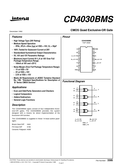
J
C D
5 6
4
K
Description
The CD4030BMS types consist of four independent Exclusive-OR gates. The CD4030BMS provides the system designer with a means for direct implementation of the Exclusive-OR function. The CD4030BMS is supplied in these 14-lead outline packages: Braze Seal DIP H4H Frit Seal DIP H1B Ceramic Flatpack H3W
A 1 B 2 J=A⊕B 3 K=C⊕D 4 C 5 D 6 VSS 7
14 VDD 13 H 12 G 11 M = G ⊕ H 10 L = E ⊕ F 9 F 8 E
Functional Diagram
A B 1 2 3
Applications
• Even and Odd-Parity Generators and Checkers • Logical Comparators • Adders/Subtractors • General Logic Functions
3. For accuracy, voltage is measured differentially to VDD. Limit is 0.050V max.
7-318
Specifications CD4030BMS
TABLE 2. AC ELECTRICAL PERFORMANCE CHARACTERISTICS GROUP A SUBGROUPS TEMPERATURE 9 10, 11 VDD = 5V, VIN = VDD or GND 9 10, 11 +25oC +125oC, -55oC LIMITS MIN MAX 280 378 200 270 UNITS ns ns ns ns
施耐德手册
American Buerau of Shipping (ABS) TYPE APPROVAL 95-NY-166-X
Det Norske Veritas (DNV) A-7038
第6页 共6页
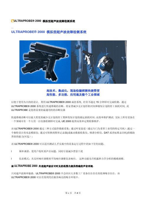
传送器: 专利的低昂音发生器
耳机: 隔噪式: 双重耳机线的单音, 阻抗 16 ohms. 超过 23dB 噪声衰减. 满足或超过 ANSI 规范和 OSHA 标准
指示器: 弹射式输出表: 载入相关测量的 0-100 的线形校正范围. 仪表全量程精度 1% . 低电池 LED 显示以便保持主
第5页 共6页
生频率大于 20KHz 的空载超声波。
l
当转动机械由于润滑不当、过载等原因造成磨损时,这种情况的发生一定伴有空
载超声波。
l
电弧,爬电和电晕放电都是电气设备失效的先兆,这些失效的先兆同时会伴有空
载超声波。
超声波多功能探测仪采用一种超声波接收探头,探测空载超声波信号并黑心换成人耳能听到的声音,并反映到指示 表头上。
机内部电源供应
电池: 自载镍镉充电. 充电系统电压:标准 110V. 同样在 220V.有效 特性: 频率调谐调整盘: 范围 20-100 kHz , 对于超窄的频率响应带有'定波段' 位置 为对数和线性表标度调整的双峰米开关 为图形记录器输出可选的辅助模式选项: 0 - 50 mV, 用于限定增益调整的带有数字校准灵敏精密增量的十转调整盘 finite gain adjustment. 灵敏度控制, 一个十转数字校准可调电位器. 弹簧支撑触发器开关 外形尺寸: 全套仪器包在一个 Zero Haliburton 铝制箱: 15' x 22' x 7' (38.1 x 55.9 x 17.8 cm). 手枪 2 lbs (.9kg). 全 套: 14 lbs (6.4 kg). 灵敏度: 50 英尺内检测 .005' (.127 mm) dia. 泄漏 @ 5 psi (.34 bar) (15.24 m). 临界值*: 1 X 10-² 1 X 10-³ std. cc/sec. freon 保固: 5 年零件/工时 *取决于配置 ULTRAPROBE 2000 仪器包符合和超越 ASTM E1002-93 泄漏检测要求. 政府代码 NSN: 6635-01-156-3927 FSCM (CAGE) Code: 59202 误差表 #s: 788, 404, 576, 583, 607 包含以下专利: 4416145, EP015115, 502674183 安全认证
IC集成电路型号大全及40系列芯片功能大全

IC集成电路型号大全及40系列芯片功能大全CD4001 四2输入端或者非门CD4002 双4输入端或者非门CD4006 18位串入/串出移位寄存器CD4007 双互补对加反相器CD4008 4位超前进位全加器CD4009 六反相缓冲/变换器CD4010 六同相缓冲/变换器CD4011 四2输入端与非门CD4012 双4输入端与非门CD4013 双主-从D型触发器CD4014 8位串入/并入-串出移位寄存器CD4015 双4位串入/并出移位寄存器CD4016 四传输门CD4017 十进制计数/分配器CD4018 可预制1/N计数器CD4019 四与或者选择器CD4020 14级串行二进制计数/分频器CD4021 08位串入/并入-串出移位寄存器CD4022 八进制计数/分配器CD4023 三3输入端与非门CD4024 7级二进制串行计数/分频器CD4025 三3输入端或者非门CD4026 十进制计数/7段译码器CD4027 双J-K触发器CD4028 BCD码十进制译码器CD4029 可预置可逆计数器CD4030 四异或者门CD4031 64位串入/串出移位存储器CD4032 三串行加法器CD4033 十进制计数/7段译码器CD4034 8位通用总线寄存器CD4035 4位并入/串入-并出/串出移位寄存CD4038 三串行加法器CD4040 12级二进制串行计数/分频器CD4041 四同相/反相缓冲器CD4042 四锁存D型触发器CD4043 三态R-S锁存触发器("1"触发)CD4044 四三态R-S锁存触发器("0"触发)CD4046 锁相环CD4047 无稳态/单稳态多谐振荡器CD4048 四输入端可扩展多功能门CD4049 六反相缓冲/变换器CD4050 六同相缓冲/变换器CD4051 八选一模拟开关CD4052 双4选1模拟开关CD4053 三组二路模拟开关CD4054 液晶显示驱动器CD4055 BCD-7段译码/液晶驱动器CD4056 液晶显示驱动器CD4059 “N”分频计数器 NSC/TICD4060 14级二进制串行计数/分频器CD4063 四位数字比较器CD4066 四传输门CD4067 16选1模拟开关CD4068 八输入端与非门/与门CD4069 六反相器CD4070 四异或者门CD4071 四2输入端或者门CD4072 双4输入端或者门CD4073 三3输入端与门CD4075 三3输入端或者门CD4076 四D寄存器CD4077 四2输入端异或者非门CD4078 8输入端或者非门/或者门CD4081 四2输入端与门CD4082 双4输入端与门CD4085 双2路2输入端与或者非门CD4086 四2输入端可扩展与或者非门CD4089 二进制比例乘法器CD4093 四2输入端施密特触发器CD4095 三输入端J-K触发器CD4096 三输入端J-K触发器CD4097 双路八选一模拟开关CD4098 双单稳态触发器CD4099 8位可寻址锁存器CD40100 32位左/右移位寄存器CD40101 9位奇偶较验器CD40102 8位可预置同步BCD减法计数器CD40103 8位可预置同步二进制减法计数器CD40104 4位双向移位寄存器CD40105 先入先出FI-FD寄存器CD40106 六施密特触发器CD40107 双2输入端与非缓冲/驱动器CD40108 4字×4位多通道寄存器CD40109 四低-高电平位移器CD40110 十进制加/减,计数,锁存,译码驱动CD40147 10-4线编码器CD40160 可预置BCD加计数器CD40161 可预置4位二进制加计数器CD40162 BCD加法计数器CD40163 4位二进制同步计数器CD40174 六锁存D型触发器CD40175 四D型触发器CD40181 4位算术逻辑单元/函数发生器CD40182 超前位发生器CD40192 可预置BCD加/减计数器(双时钟) CD40193 可预置4位二进制加/减计数器CD40194 4位并入/串入-并出/串出移位寄存CD40195 4位并入/串入-并出/串出移位寄存CD40208 4×4多端口寄存器CD4501 4输入端双与门及2输入端或者非门CD4502 可选通三态输出六反相/缓冲器CD4503 六同相三态缓冲器CD4504 六电压转换器CD4506 双二组2输入可扩展或者非门CD4508 双4位锁存D型触发器CD4510 可预置BCD码加/减计数器CD4511 BCD锁存,7段译码,驱动器CD4512 八路数据选择器CD4513 BCD锁存,7段译码,驱动器(消隐) CD4514 4位锁存,4线-16线译码器CD4515 4位锁存,4线-16线译码器CD4516 可预置4位二进制加/减计数器CD4517 双64位静态移位寄存器CD4518 双BCD同步加计数器CD4519 四位与或者选择器CD4520 双4位二进制同步加计数器CD4521 24级分频器CD4522 可预置BCD同步1/N计数器CD4526 可预置4位二进制同步1/N计数器CD4527 BCD比例乘法器CD4528 双单稳态触发器CD4529 双四路/单八路模拟开关CD4530 双5输入端优势逻辑门CD4531 12位奇偶校验器CD4532 8位优先编码器CD4536 可编程定时器CD4538 精密双单稳CD4539 双四路数据选择器CD4541 可编程序振荡/计时器CD4543 BCD七段锁存译码,驱动器CD4544 BCD七段锁存译码,驱动器CD4547 BCD七段译码/大电流驱动器CD4549 函数近似寄存器CD4551 四2通道模拟开关CD4553 三位BCD计数器CD4555 双二进制四选一译码器/分离器CD4556 双二进制四选一译码器/分离器CD4558 BCD八段译码器CD4560 "N"BCD加法器CD4561 "9"求补器CD4573 四可编程运算放大器CD4574 四可编程电压比较器CD4575 双可编程运放/比较器CD4583 双施密特触发器CD4584 六施密特触发器CD4585 4位数值比较器CD4599 8位可寻址锁存器CD22100 4×4×1交叉点开关0206A 天线开关集成电路03VFG9 发射压控振荡集成电路1021AC 发射压控振荡集成电路1097C 升压集成电路140N 电源取样比较放大集成电路14DN363 伺服操纵集成电路15105 充电操纵集成电路15551 管理卡升压集成电路1710 视频信号处理集成电路1N706 混响延时集成电路20810-F6096 存储集成电路2252B 微处理集成电路2274 延迟集成电路24C01ACEA 存储集成电路24C026 存储集成电路24C04 存储集成电路24C64 码片集成电路24LC16B 存储集成电路24LC65 电可改写编程只读存储集成电路27C1000PC-12 存储集成电路27C2000QC-90 存储集成电路27C20T 存储集成电路27C512 电可改写编程只读存储集成电路2800 红外遥控信号接收集成电路28BV64 码片集成电路28F004 版本集成电路31085 射频电源集成电路32D54 电源、音频信号处理集成电路1732D75 电源、音频信号处理集成电路32D92 电源中频放大集成电路4066B 电子开关切换集成电路4094 移位寄存串入、并出集成电路424260SDJ 存储集成电路4260 动态随机存储集成电路4270351/91B9905 中频放大集成电路4370341/90M9919 中频处理集成电路4464 存储集成电路4558 双运算放大集成电路4580D 双运算放大集成电路47C1638AN-U337 微处理集成电路47C1638AU-353 微处理集成电路47C432GP 微处理集成电路47C433AN-3888 微处理集成电路49/4CR1A 中频放大集成电路5101 天线开关集成电路5G052 发光二极管四位显示驱动集成电路5G24 运算放大集成电路5W01 双运算放大集成电路649/CRIA70612 中频放大集成电路673/3CR2A 多模转换集成电路74122 可重触发单稳态集成电路74HC04 逻辑与非门集成电路74HC04D 六反相集成电路74HC123 单稳态集成电路74HC125 端口功能扩展集成电路74HC14N 六反相集成电路74HC157A 多路转换集成电路74HC165 移相寄存集成电路1874HC245 总线收发集成电路74HC32 或者门四2输入集成电路74HC374八D 触发集成电路74HC573D 存储集成电路74HCT157 多路转换双输入集成电路74HCT4046A 压控振荡集成电路74HCT4538D 单稳态集成电路74HCT4538N 触发脉冲集成电路74HCT86D 异或者门四2输入集成电路74HCU04 与非门集成电路74LS125 端口功能扩展集成电路74LS373 锁存集成电路74LS393 计数双四位二进制集成电路74LS74双D 触发集成电路78014DFP 系统操纵处理集成电路811N 伴音阻容偏置集成电路83D33 压控振荡集成电路85712 场扫描信号校正处理集成电路85713 行扫描信号校正集成电路87C52 微处理集成电路87CK38N-3584 微处理集成电路87CK38N-3627 微处理集成电路89C52 系统操纵处理集成电路89C55 系统操纵处理集成电路93C66 电可改写编程只读存储集成电路93LC56 电可改写编程存储集成电路9821K03 系统操纵集成电路A1642P 背景歌声消除集成电路A701 红外遥控信号接收集成电路A7950 场频识别集成电路19A8772AN 色差信号延迟处理集成电路A9109 功率放大集成电路AAB 电源集成电路ACA650 色度信号解调集成电路ACFP2 色度、亮度信号分离集成电路ACP2371 多伴音、多语言改善集成电路ACVP2205 色度、亮度信号分离集成电路AD1853 立体声数/模转换集成电路AD1858 音频解调集成电路AD722 视频编码集成电路ADC2300E 音频数/模转换集成电路ADC2300J 音频数/模转换集成电路ADC2310E 音频数/模转换集成电路ADV7172 视频编码集成电路ADV7175A 视频编码集成电路AE31201 频率显示集成电路AJ7080 射频调制集成电路AK4321-VF-E1 音频数/模转换集成电路AN1319 双高速电压比较集成电路AN1358S 双运算放大集成电路AN1393 双运算放大集成电路AN1431T 稳压电源集成电路AN1452 音频前置放大集成电路AN1458S 双运算放大集成电路AN206 伴音中频及前置放大集成电路AN222 自动频率操纵集成电路AN236 副载波信号处理集成电路AN239Q 图像、伴音中频放大集成电路AN247P 图像中频放大、AGC操纵集成电路AN253P 调频/调幅中频放大集成电路20AN262 音频前置放大集成电路AN2661NK 视频信号处理集成电路AN2663K 视频信号处理集成电路AN272 音频功率放大集成电路AN2751FAP 视频信号处理集成电路AN281 色度解码集成电路AN2870FC 多功能操纵集成电路AN295 行、场扫描信号处理集成电路AN301 伺服操纵集成电路AN305 视频自动增益操纵集成电路AN306 色度自动相位操纵集成电路AN318 直流伺服操纵集成电路AN320 频率操纵、调谐显示驱动集成电路AN3215K 视频信号处理集成电路AN3215S 视频信号处理集成电路AN3224K 磁头信号记录放大集成电路AN3248NK 亮度信号记录、重放处理集成电路AN331 视频信号处理集成电路AN3311K 磁头信号放大集成电路AN3313 磁头信号放大集成电路AN3321S 录像重放信号处理集成电路AN3331K 磁头信号处理集成电路AN3337NSB 磁头信号放大集成电路AN3380K 磁头信号处理集成电路AN3386NK 磁头信号处理集成电路AN3495K 色度、亮度信号降噪集成电路AN355 伴音中频放大、检波集成电路AN3581S 视频驱动集成电路AN366 调频/调幅中频放大集成电路AN3791 移位操纵集成电路21AN3792 磁鼓伺服操纵接口集成电路AN3795 主轴伺服操纵接口集成电路AN3814K 电机驱动集成电路AN4265 音频功率放大集成电路AN4558 运算放大集成电路AN5010 电子选台集成电路AN5011 电子选台集成电路AN5015K 电子选台集成电路AN5020 红外遥控信号接收集成电路AN5025S 红外遥控信号接收集成电路AN5026K 红外遥控信号接收集成电路AN5031 电调谐操纵集成电路AN5034 调谐操纵集成电路AN5036 调谐操纵集成电路AN5043 调谐操纵集成电路AN5071 频段转换集成电路AN5095K 电视信号处理集成电路AN5110 图像中频放大集成电路AN5130 图像中频、视频检波放大集成电路AN5138NK 图像、伴音中频放大集成电路AN5156K 电视信号处理集成电路AN5177NK 图像、伴音中频放大集成电路AN5179K 图像、伴音中频放大集成电路AN5183K 中频信号处理集成电路AN5195K 中频、色度、扫描信号处理集成电路AN5215 伴音信号处理集成电路AN5520 伴音中频放大及鉴频集成电路AN5222 伴音中频放大集成电路AN5250 伴音中频放大、鉴频及功率放大集成电路AN5262 音频前置放大集成电路22AN5265 音频功率放大集成电路AN5270 音频功率放大集成电路AN5273 双声道音频功率放大集成电路AN5274 双声道音频功率放大集成电路AN5275 中置、3D放大集成电路AN5285K 双声道前置放大集成电路AN5295NK 音频信号切换集成电路AN5312 视频、色度信号处理集成电路AN5313NK 视频、色度信号处理集成电路AN5342 图像水平轮廓校正集成电路AN5342FB 水平清晰度操纵集成电路AN5344FBP 色度信号处理集成电路AN5348K 人工智能信号处理集成电路AN5385K 色差信号放大集成电路AN5410 行、场扫描信号处理集成电路AN5421 同步检测集成电路AN5422 行、场扫描信号处理集成电路AN5512 场扫描输出集成电路AN5515 场扫描输出集成电路AN5521 场扫描输出集成电路AN5532 场扫描输出集成电路AN5534 场扫描输出集成电路AN5551 枕形校正集成电路AN5560 场频识别集成电路AN5600K 中频、亮度、色度及扫描信号处理集成电路AN5601K 视频、色度、同步信号处理集成电路AN5607K 视频、色度、行场扫描信号处理集成电路AN5615 视频信号处理集成电路AN5620X 色度信号处理集成电路AN5621 场扫描输出集成电路23AN5625 色度信号处理集成电路AN5633K 色度信号处理集成电路AN5635 色度解码集成电路AN5635NS 色度解码集成电路AN5637 色度解码、亮度延迟集成电路AN5650 同步信号分离集成电路AN5682K 基色电子开关切换集成电路AN5693K 视频、色度、行场扫描信号处理集成电路AN5712 图像中频放大、AGC操纵集成电路AN5722 图像中频放大、检波集成电路AN5732 伴音中频放大、鉴频集成电路AN5743 音频功率放大集成电路AN5750 行自动频率操纵及振荡集成电路AN5757S 行扫描电源电压操纵集成电路AN5762 场扫描振荡、输出集成电路AN5764 光栅水平位置操纵集成电路AN5765 电源稳压操纵集成电路AN5767 同步信号处理集成电路AN5768 光栅倾斜校正操纵集成电路AN5769 行、场会聚操纵集成电路AN5790N 行扫描信号处理集成电路AN5791 同步脉冲相位与脉宽调整集成电路AN5803 双声道立体声解调集成电路AN5836 双声道前置放大集成电路AN5858K 视频信号操纵集成电路AN5862 视频信号操纵集成电路AN5862S-E1 视频信号开关操纵集成电路AN5870K 模拟信号切换集成电路AN5891K 音频信号处理集成电路AN614 行枕形校正集成电路24AN6210 双声道前置放大集成电路AN6306S 亮度信号处理集成电路AN6308 模拟电子开关集成电路AN6327 视频重放信号处理集成电路AN6341N 伺服操纵集成电路AN6342N 基准分频集成电路AN6344 伺服操纵集成电路AN6345 分频集成电路AN6346N 磁鼓伺服操纵集成电路AN6350 磁鼓伺服操纵集成电路AN6357N 主轴接口集成电路AN6361N 色度信号处理集成电路AN6367NK 色度信号处理集成电路AN6371S 自动相位操纵集成电路AN6387 电机伺服操纵集成电路AN6550 卡拉OK音频放大集成电路AN6554 四运算放大集成电路AN6561 双运算放大集成电路AN6562SG 双运算放大集成电路AN6609N 电机驱动集成电路AN6612 电机稳速操纵集成电路AN6650 电机速度操纵集成电路AN6651 电机速度操纵集成电路AN6652 电机稳速操纵集成电路AN6875 发光二极管五位显示驱动集成电路AN6877 发光二极管七位显示驱动集成电路AN6884 发光二极管五位显示驱动集成电路AN6886 发光二极管五位显示驱动集成电路AN6888 发光二极管显示驱动集成电路AN6914 双电压比较集成电路25AN7085N5 单片录、放音集成电路AN7105 双声道音频功率放大集成电路AN7106K 双声道音频功率放大集成电路AN7108 单片立体声放音集成电路AN710S 单片放音集成电路AN7110E 音频功率放大集成电路AN7114 音频功率放大集成电路AN7116 音频功率放大集成电路AN7118 双声道音频功率放大集成电路AN7118S 双声道音频功率放大集成电路AN7120 音频功率放大集成电路AN7124 双声道音频功率放大集成电路AN7145 双声道音频功率放大集成电路AN7148 双声道音频功率放大集成电路AN7158N 音频功率放大7.5W×2集成电路AN7161N 音频功率放大集成电路AN7164 双声道音频功率放大集成电路AN7171NK 音频功率放大集成电路AN7205 调频/调谐及高频放大集成电路AN7220 调频/调幅中频放大集成电路AN7222 调频/调幅中频放大集成电路AN7223 调频/调幅中频放大集成电路AN7226 调频/调幅中频放大集成电路AN7256 调频/调谐及中频放大集成电路AN7311 双声道前置放大集成电路AN7312 双声道前置放大集成电路AN7315 双声道前置放大集成电路AN7315S 双声道前置放大集成电路AN7320 音频前置放大集成电路AN7396K 双声道前置放大集成电路26AN7397K 双声道前置放大集成电路AN7410 调频立体声多路解码集成电路AN7414 调频立体声解码集成电路AN7420N 调频立体声解码集成电路AN7470 调频立体声解码集成电路AN7805 三端电源稳压+5V/1A集成电路AN7806 三端电源稳压+6V/1A集成电路AN7807 三端电源稳压+7V/1A集成电路AN7808 三端电源稳压+8V/1A集成电路AN7809 电源稳压+9V/1A集成电路AN7810 三端电源稳压+10V/1A集成电路AN7812 三端电源稳压+12V/1A集成电路AN7815 三端电源稳压+15V/1A集成电路AN7818 三端电源稳压+18V/1A集成电路AN7820 三端电源稳压+20V/1A集成电路AN7824 三端电源稳压+24V/1A集成电路AN78L05 三端电源稳压+5V/0.1A集成电路AN78L06 三端电源稳压+6V/0.1A集成电路AN78L08 三端电源稳压+8V/0.1A集成电路AN78L09 三端电源稳压+9V/0.1A集成电路AN78L10 三端电源稳压+10V/0.1A集成电路AN78L12 三端电源稳压+12V/0.1A集成电路AN78L15 三端电源稳压+15V/0.1A集成电路AN78L18 三端电源稳压+18V/0.1A集成电路AN78L20 三端电源稳压+20V/0.1A集成电路AN78L24 三端电源稳压+24V/0.1A集成电路AN78M05 三端电源稳压+5V/0.5A集成电路AN78M06 三端电源稳压+6V/0.5A集成电路AN78M08 三端电源稳压+8V/0.5A集成电路AN78M09 三端电源稳压+9V/0.5A集成电路27AN78M10 三端电源稳压+10V/0.5A集成电路AN78M12 三端电源稳压+12V/0.5A集成电路AN78M15 三端固定式稳压+15V/0.5A集成电路AN78M18 三端电源稳压+18V/0.5A集成电路AN78M20 三端电源稳压+20V/0.5A集成电路AN78M24 三端电源稳压+24V/0.5A集成电路AN7905 三端电源稳压-5V/1A集成电路AN7906 三端电源稳压-6V/1A集成电路AN7908T 三端电源稳压-8V/1A集成电路AN7909T 三端电源稳压-9V/1A集成电路AN7910T 三端电源稳压-10V/1A集成电路AN7912 三端电源稳压-12V/1A集成电路AN7915 三端电源稳压-15V/1A集成电路AN7918 三端电源稳压-18V/1A集成电路AN7920 三端电源稳压-20V/1A集成电路AN7924 三端电源稳压-24V/1A集成电路AN79L05 三端电源稳压-5V/0.1A集成电路AN79L06 三端电源稳压-6V/0.1A集成电路AN79L08 三端电源稳压-8V/0.1A集成电路AN79L09 三端电源稳压-9V/0.1A集成电路AN79L10 三端电源稳压-10V/0.1A集成电路AN79L12 三端电源稳压-12V/0.1A集成电路AN79L15 三端电源稳压-15V/0.1A集成电路AN79L18 三端电源稳压-18V/0.1A集成电路AN79L20 三端电源稳压-20V/0.1A集成电路AN79L24 三端电源稳压-24V/0.1A集成电路AN79M05 三端电源稳压-5V/0.5A集成电路AN79M06 三端电源稳压-6V/0.5A集成电路AN79M08 三端电源稳压-8V/0.5A集成电路AN79M09 三端电源稳压-9V/0.5A集成电路28AN79M10 三端电源稳压-10V/0.5A集成电路AN79M12 三端电源稳压-12V/0.5A集成电路AN79M15 三端电源稳压-15V/0.5A集成电路AN79M18 三端电源稳压-18V/0.5A集成电路AN79M20 三端电源稳压-20V/0.5A集成电路AN79M24 三端电源稳压-24V/0.5A集成电路AN8028 自激式开关电源操纵集成电路AN8270K 主轴电机操纵集成电路AN8280 电机驱动集成电路AN8281S 电机驱动集成电路AN8290S 主轴电机驱动集成电路AN8355S 条形码扫描接收集成电路AN8370S 光电伺服操纵集成电路AN8373S 射频伺服处理集成电路AN8375S 伺服处理集成电路AN8389S-E1 电机驱动集成电路AN8480NSB 主轴电机驱动集成电路AN8481SB-E1 主轴电机驱动集成电路AN8482SB 主轴电机驱动集成电路AN8623FBQ 主轴伺服处理集成电路AN8788FB 电机驱动集成电路AN8802CE1V 伺服处理集成电路AN8813NSBS 主轴电机驱动集成电路AN8819NFB 伺服驱动、直流交换集成电路AN8824FBQ 前置放大集成电路AN8825NFHQ-V 聚焦、循迹误差处理集成电路AN8831SC 视频预视放集成电路AN8832SB-E1 射频放大、伺服处理集成电路AN8837SB-E1 伺服处理集成电路AN89C2051-24PC 微处理集成电路29APU2400U 音频信号处理集成电路APU2470 音频信号处理集成电路AS4C14405-60JC 动态随机存储1M×4集成电路AS4C256K16ED-60JC 存储集成电路ASD0204-015 图文操纵集成电路ASD0204GF-022-3BA显示操纵集成电路AT24C08 存储集成电路AT24C08A 存储集成电路AT24C256-10CI 码片集成电路AT27C010 电可改写编程只读存储集成电路AT27C020 存储集成电路ATMEL834 存储集成电路AVM-1 视频信号处理厚膜集成电路AVM-2 音频信号处理厚膜集成电路AVSIBCP08 倍压整流切换集成电路B0011A 存储集成电路B1218 电子快门操纵集成电路BA033T 三端电源稳压+3.3V集成电路BA10324 四运算放大集成电路BA10393N 双运算放大集成电路BA1102F 杜比降噪处理集成电路BA1106F 杜比降噪处理集成电路BA12ST 电源稳压集成电路BA1310 调频立体声解码集成电路BA1332L 调频立体声解码集成电路BA1350 调频立体声解码集成电路BA1351 调频立体声解码集成电路BA1356 调频立体声解码集成电路BA1360 调频立体声解码集成电路BA15218N 双运算放大集成电路30BA225 可触发双单稳态振荡集成电路BA302 音频前置放大集成电路BA311 音频前置放大集成电路BA313 音频前置放大集成电路BA3283 单片放音集成电路BA328F 双声道前置放大集成电路BA329 双声道前置放大集成电路BA3304F 录放音前置均衡放大集成电路BA3306 音频、前置放大集成电路BA3312N 话筒信号前置放大集成电路BA3313L 自动音量操纵集成电路BA3314 话筒信号前置放大集成电路BA335 自动选曲集成电路BA336 自动选曲集成电路BA340 音频前置放大集成电路BA3402F 双声道前置放大集成电路BA3404F 自返转放音集成电路BA343 双声道前置放大集成电路BA3503F 双声道前置放大集成电路BA3506 单片放音集成电路BA3513FS 单片放音集成电路BA3516 单片放音集成电路BA3706 自动选曲集成电路BA3707 录音带曲间检测集成电路BA3812L 五频段音调补偿集成电路BA3818F 电压比较运放集成电路BA3822LS 双声道五频段显示均衡集成电路BA3828 电子选台预置集成电路BA3880 音频处理集成电路31BA401 调频中频放大集成电路BA402 调频中频放大集成电路BA4110 调频中频放大集成电路BA4234L 调频中频放大集成电路BA4402 调频调谐收音集成电路BA4403 调频高频放大、混频、本振集成电路BA4560 双运算放大集成电路BA5096 数字混响集成电路BA5102A 音频功率放大集成电路BA514 音频功率放大集成电路BA516 音频功率放大集成电路BA5208AF 音频功率放大集成电路BA532 音频功率放大集成电路BA534 音频功率放大集成电路BA5406 双声道音频功率放大集成电路BA5412 音频功率放大集成电路BA547 音频功率放大1.5W集成电路BA5912AFP-YE2 电机驱动、倾斜、加载集成电路BA5981FP-E2 聚焦、循迹驱动集成电路BA5983FB 四通道伺服驱动集成电路BA5983FM-E2 电机驱动集成电路BA6104 发光二极管五位显示驱动集成电路BA6107A 电机伺服操纵集成电路BA6109 加载电机驱动集成电路BA6125 发光二极管五位显示驱动集成电路BA6137 发光二极管五位显示驱动集成电路BA6191 音频操纵集成电路BA6196FP 伺服驱动集成电路BA6208 电机驱动集成电路BA6208D 电机驱动集成电路32BA6209 电机驱动集成电路BA6209N 双向驱动电机集成电路BA6218 加载电机驱动集成电路BA6219 电机驱动集成电路BA6219B 电机驱动集成电路BA6227 电机稳速操纵集成电路BA6238 电机驱动集成电路BA6239 电机双向驱动集成电路BA6239A 电机双向驱动集成电路BA6246M 加载、转盘电机驱动集成电路BA6248 电机驱动集成电路BA6286 电机驱动集成电路BA6287 电机驱动集成电路BA6290 电机驱动集成电路BA6295AFP-E2 加载、倾斜驱动集成电路BA6296FP 电机速度操纵集成电路BA6297AFP 伺服驱动集成电路BA6302A 电机伺服操纵集成电路BA6305 操纵放大集成电路BA6305F 操纵放大集成电路BA6308 电子开关切换集成电路BA6321 电机伺服操纵集成电路BA6392 伺服驱动集成电路BA6395 主轴电机驱动集成电路BA6396FP 伺服驱动集成电路BA6411 电机驱动集成电路BA6435S 主轴电机驱动集成电路BA6459P1 电机驱动集成电路BA6570FP-E2 聚焦、循迹驱动集成电路33BA6664FM 三相主电机驱动集成电路BA6791FP 四通道伺服驱动集成电路BA6796FP 电机驱动集成电路BA6810S 音频显示驱动集成电路BA6844AFP-E2 三相主电机驱动集成电路BA6849FP 主轴电机驱动集成电路BA689 发光二极管十二位显示驱动集成电路BA6893KE2 直流变换驱动集成电路BA6956AN 加载电机驱动集成电路BA6993 双运算放大集成电路BA7001 音频切换集成电路BA7004 测试信号发生集成电路BA7005AL 射频调制集成电路BA7007 信号检测集成电路BA7021 视频信号选择集成电路BA7024 视频信号测试集成电路BA7025L 信号检测集成电路BA7042 振荡集成电路BA7047 调频检波集成电路BA7048N 包络信号检测集成电路BA7106LS 检测信号操纵集成电路BA7180FS 磁头信号放大集成电路BA7212S 磁头信号放大集成电路BA7253S 磁头信号放大集成电路BA7254S 四磁头信号放大集成电路BA7258AS 亮度信号处理集成电路BA7264S 视频信号处理集成电路BA7274S 磁头信号放大集成电路BA7357S 中频放大集成电路BA7604N 电子开关切换集成电路34BA7606F 色差信号切换集成电路BA7655 色度信号处理集成电路BA7665FS-E2 视频输出放大集成电路BA7725FS 混响立体声放大集成电路BA7725S 信号压缩及扩展处理集成电路BA7743FS 磁头信号放大集成电路BA7751ALS 音频信号录放处理集成电路BA7752LS 音频信号处理集成电路BA7755 磁头开关集成电路BA7755AF-E2 磁头开关集成电路BA7765AS 音频信号处理集成电路BA7766SA 音频信号处理集成电路BA7767AS 音频信号处理集成电路BA7797F 音频信号处理集成电路BA8420 特技操纵处理集成电路BAL6309 场同步信号发生集成电路BH3866AS 音频、色度信号前置放大集成电路BH4001 微处理集成电路BH7331P 音频功率放大集成电路BH7770KS 音频信号处理集成电路BL3207 亮度延时集成电路BL3208B 音频延迟混响集成电路BL5132 中频放大集成电路BL54573 电子调频波段转换集成电路BL5612 视频放大、色差矩阵集成电路BM5060 微处理集成电路BM5061 字符发生集成电路BM5069 微处理集成电路BN5115 图像中频放大集成电路BOC31F 单片微处理集成电路35BP5020 视频电源转换集成电路BT852 视频编码集成电路BT864 视频编码集成电路BT866PQFP 微处理集成电路BU12102 时序信号发生解码集成电路BU2092F 扩展集成电路BU2185F 同步信号处理集成电路BU2285FV 时钟信号发生集成电路BU2820 伺服操纵集成电路BU2841FS 视频、蓝背景信号发生集成电路BU2872AK 操作系统操纵、屏显驱动集成电路BU3762AF 红外遥控信号发射集成电路BU4053B 电子开关切换集成电路BU5814F 红外遥控信号发射集成电路BU5994F 红外遥控信号发射集成电路BU6198F 屏幕显示集成电路BU9252F 音频延时集成电路BU9252S 数/模转换集成电路BU9253FS 话筒音频混响集成电路BX1303 音频功率放大集成电路BX1409 红外遥控信号接收集成电路BX7506 主轴电机电源操纵集成电路C1363CA 红外遥控电子选台集成电路C1490HA 红外遥控信号接收集成电路C187 分配、十进制计数集成电路C301 译码BCD-10段集成电路C68639Y 微处理集成电路C75P036 微处理集成电路CA0002 调幅模拟声解调集成电路CA2004 音频功率放大集成电路36CA2006 音频功率放大集成电路CA270AW 视频检波放大集成电路CA3075 调频中频放大集成电路CA3089 调频中频放大集成电路CA3120E 视频信号处理集成电路CA3140 运算放大集成电路CA810 音频功率放大集成电路CA920 行扫描信号处理集成电路CAS126 天线开关集成电路CAT24C16 电可改写编程只读存储集成电路CAT35C104HP 存储集成电路CC4000 或者非门双3输入集成电路CC4008 计数4位二进制集成电路CC40107 与非双2输入缓冲、驱动集成电路CC40174 六D触发集成电路CC40194 移位寄存集成电路CC4025 或者非门3输入集成电路CC4026 译码、驱动、十进制计数集成电路CC4027 上升沿J-K触发集成电路。
TI 便携式媒体播放器解决方案
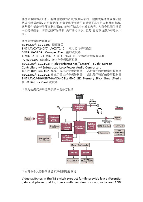
便携式多媒体点唱机,有时也被称为音频/视频点唱机,便携式媒体播放器或便携式视频播放器,为消费类和消费类电子制造厂商提供了具有巨大利益的市场。
这些器件都是基于硬盘驱动器的,能够存储几个小时的内容,为当今忙碌生活的人们提供娱乐。
尽管这些产品的相关市场还很小,但是,它的市场潜力却是很大的。
便携式媒体组成器件为:TS5V330/TS3V330:视频开关SN74AVCXT245/74LVCXT245:双电源电平转换器SN74LV4320A:CompactFlash接口收发器TLV320AIC32/TLV320AIC31:低功耗、立体声音频编解码器PCM3792A:低功耗、立体声音频编解码器TSC2100/TSC2102: High-Performance “Smart” Touch- Screen Controllers w/ Integrated Low-Power Audio ConvertersTSC2100/TSC2102:集成了低功耗音频转换器高性能”智能”触摸屏控制器TSC2301/TSC2302:集成了低功耗音频转换器高性能”智能”触摸屏控制器SN74AVCA406/SN74AVCA406L:MMC,SD,Memory Stick,SmartMedia 和xD-Picture Card收发器下图为便携式多功能数字媒体设备方框图下面对各个元器件的性能和方框图进行描述:Video switches in the TS switch product family provide low differential gain and phase, making these switches ideal for composite and RGBvideo applications. TS video switches also offer the wide bandwidth and low crosstalk required to support high-frequency video applications.Key Features*Low differential gain and phase (3-V DG = 0.82%, DP = 0.1 degrees typ) (5-V DG = 0.64%, DP = 0.1 degrees typ)*Wide bandwidth (BW = 300 MHz min)*Low crosstalk (3-V XTALK = –80 dB typ) (5-V XTALK = –63 dB typ) *Low-power consumption (ICC = 3 A max)*Bidirectional data flow, with near-zero propagation delay*Low ON-state resistance (ron = 3 typ)*Rail-to-rail switching on data I/O ports (0 to VCC)*Ioff supports partial-power-down mode operation*Suitable for both RGB and composite-video switching Applications*Composite and RGB video多路视频信号从视频处理器到VGA卡两个外接视频端口Dual-supply level shifters are the ideal solution for bidirectional level translation. These devices have two separate VCC supplies, one for each port (VCCA and VCCB), which gives them flexibility to operate in mixed-mode applications. These dual-supply devices allow for bidirectional level translation between different voltage nodes from 1.2 V to 3.6 V and 1.65 V to 5.5 V. TI also offers a wide range ofbit-width options.TI’s Dual-Supply Level-Translation Portfolio扩展系列双电源电平转换设备This CompactFlash (CF) interface chip is designed to provide a singlechip solution for CF card interfaces. Separate VCC rails for the system bus side and the CF connector bus side allow voltage-level shifting.This is helpful for interfacing between a core chipset, which may operatefrom 3.3 V down to 1.65 V, and CF cards with 3.3-V or 5-V supply voltages.Key Features*Level translation supports both 3.3- and 5-V CompactFlash cards *High degree of integration*Schmidt-trigger inputs for CompactFlash control signals*Ioff and /MASTER_EN (shutdown) pin*Internal decode logic for direction control (DIR)*Robust ESD protection (+8-kV HBM) on card pinsApplications*PDAs*Handheld scanners*Set-top boxes*Network equipmentSN74LV4320A典型应用示意图]The TLV320AIC32/TLV320AIC31 are highly integrated, low-power stereo CODECs for use in a variety of portable audio equipment. The TLV320AIC32 includes six single-ended analog inputs. TheTLV320AIC31 includes two single-ended analog inputs and two differential analog inputs. Both CODECs have six output drivers. They also include two line output drivers and four high-power amplifiers that can be configured as stereo headphone drivers or stereo speaker drivers.Key Features*Stereo DAC (100 dBA) and ADC (92 dBA) support rates up to 96 kSPS*14-mW power dissipation with stereo playback at 48 kSPS*Stereo headphone drivers and 500-mW, 8speaker driver*Stereo microphone preamps and hardware automatic gain control *Integrated PLL for flexible audio clock generation*Programmable digital audio bass/treble/EQ with 3D effects*Analog inputs are configurable as single-ended (AIC32/AIC31) or fully differential (AIC31 only)*Up to six analog inputs, six output drivers for easy connectivity to multiple devices in a cellular telephony system*Packaging: 5 5 mm 32-pin QFNApplications*Cellular and smart phones*Digital still cameras, digital video cameras*MP3 and portable media players* PDAs*Talking toys and toys with audioTLV320AIC32方框图The PCM3792A is a single-chip, 20-bit stereo audio CODEC with three single-ended analog inputs, three stereo outputs and two mono outputs. It includes an integrated stereo Class-D audio power amplifier. The PCM3792A accepts left-justified,right-justified andI2S™ data formats for simple interface to audio DSP or decoder/encoder chips. It can be controlled with a two- or threewire serial interface. The PCM3792A is suitable for a wide variety of portable applications where good performance and low power are required.Key Features*95-dB SNR DAC, 90-dB SNR ADC*Stereo 500 mW at 8 for speaker amplifier*Stereo 30 mW at 32 for headphone amplifier*+6-dB to –70-dB volume control for each analog output*+30-dB to –12-dB gain control for analog inputs*48-mW power dissipation at 3.3 V (playback)*67-mW power dissipation at 3.3 V (recording)*Auto Level Control (ALC) for playback and recording*Power supply:*1.8 to 3.6 V for digital I/O*2.7 to 3.6 V for digital and analog*2.7 to 4.5 V for speaker amplifier*Packaging: 6 6 mm BGAApplications*Mobile phones, PDAs*Video camcorders, movie digital still cameras*Portable digital audio players*Expected release April 2006.PCM3792A方框图The TSC2100 is a four-wire smart touch-screen controller (TSC) with an integrated audio CODEC, a headphone/speaker amplifier and a 12-bit battery/temperature/auxiliary measurement SAR ADC. The TSC2102 is a pin- and software-compatible version of the TSC2100, incorporating the smart four-wire TSC, a stereo audio DAC and a headphone/speaker driver.Key Features*Four-wire smart touch-screen controller*Stereo DAC and mono audio ADC (TSC2100) support up to 53 kSPS *97-dB stereo playback at 11-mW power dissipation*Audio output drivers provide 325 mW into 8 and also support stereo headphones with capless output option*Integrated PLL for flexible audio clock generation*Programmable digital audio bass/treble/EQ/de-emphasis (TSC2100 only)*Microphone preamp and hardware automatic gain control*Direct battery measurement accepts up to 6-V input*On-chip temperature and auxiliary-input measurement*Packaging:7 ×7 mm 48-pin QFN (TSC2101)5 × 5 mm 32-pin QFN (TSC2100)32-pin TSSOP (TSC2100)Applications*Portable media players*PDAs*Portable audio productsTSC2100方框图The TSC2301 is a 4-wire smart touch-screen controller (TSC) with an integrated audio codec, a headphone/speaker amplifier and a 12-bit battery/temperature/auxiliary measurement ADC. The TSC2301 includes a keypad controller and 6 additional GPIO pins.Key Features*4-wire smart touch-screen controller*4 4 keypad interface (TSC2301 only)*6 GPIO pins (TSC2301 only)*Full stereo codec supporting up to 48 kSPS*98-dB stereo playback with 27-mW power dissipation*8-bit DAC for LCD contrast control*Integrated PLL for flexible audio clock generation*27-mW stereo headphone driver with capless output option*Programmable digital audio bass/treble/EQ/de-emphasis*Microphone preamp and hardware automatic gain control*Direct battery measurement accepts up to 6-V input*On-chip temperature and auxiliary-input measurement*Packaging: 6 6 mm 120-ball BGA (TSC2301), 64-pin TQFP (TSC2301), 7 7 mm 48-pin QFN (TSC2302)Applications*Smart phones*PDAs*Portable media players*Low-power audio productsTSC2301方框图The SN74AVCA406 is a transceiver for interfacing microprocessors with MultiMediaCard (MMC), SD Secure Digital™ cards, Memory Stick-compliant products, SmartMedia cards, or xD-Picture Card. It integrates high ESD protection, which eliminates the need for external ESD diodes.Key Features*Transceiver for interface with MultiMediaCard (MMC), SD Secure Digital, Memory Stick (MS) compliant products, SmartMedia andxD-Picture Card*Configurable I/O switching levels with dual-supply pins operating over full 1.4- to 3.6-V power-supply range*A ports are placed in high-impedance state when card-side supply voltage is switched off*ESD protection for card-side pins exceeds ±15-kV air gap discharge,±8-kV contact dischargeApplications*Handsets-Digital still cameras*PDAs-Set-top boxes*Handheld scannersSN74AVCA406存储卡接口。
TI芯片资料
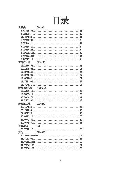
目录电源类(1-10)8.CSD19535 (18)9.INA210 (19)10.INA282 (21)1.TPS28225 (2)7.TPS4021 (16)3.TPS54340 (5)4.TPS56528 (9)5.TPS7A1601 (12)6.TPS7A4001 (14)2.UCC27211 (4)高速放大器(11-17)15.LMH6552 (31)12.LMH6703 (25)17.OPA2356 (34)13.OPA2695 (27)16.OPA842 (32)11.THS3201 (23)14.VCA821 (29)精密ADC/DAC (18-21)18.ADS1118 (36)19.DAC7811 (38)20.DAC8571 (41)21.REF3330 (43)精密放大器(22-27)22.INA333 (45)23.INA826 (46)24.OPA192 (48)25.OPA2320 (50)26.OPA2330 (52)27.OPA2376 (53)音频功放(28)28.TPA3112 (55)其他(29-33)30.SN74AUP1G07 (58)29.TLV3501 (57)33.TS12A4515 (62)31.TS5A3159 (61)32.TS5A3166 (62)零一.TPS282258引脚高频4A吸入电流同步MOSFET驱动器描述The TPS28225 and TPS28226 are high-speed drivers for N-channel complimentary driven power MOSFETs with adaptive dead-time control. These drivers are optimized for use in variety of high-current one and multi-phase dc-to-dc converters. The TPS28225/6 is a solution that provides highly efficient, small size low EMI emmissions.The performance is achieved by up to 8.8-V gate drive voltage, 14-ns adaptive dead-time control, 14-ns propagation delays and high-current 2-A source and 4-A sink drive capability. The 0.4-impedance for the lower gate driver holds the gate of power MOSFET below its threshold and ensures no shoot-through current at high dV/dt phase node transitions. The bootstrap capacitor charged by an internal diode allows use of N-channel MOSFETs in half-bridge configuration.The TPS28225/6 features a 3-state PWM input compatible with all multi-phase controllers employing 3-state output feature. As long as the input stays within 3-state window for the 250-ns hold-off time, the driver switches both outputs low. This shutdown mode prevents a load from the reversed- output-voltage.The other features include under voltage lockout, thermal shutdown and two-way enable/power good signal. Systems without 3-state featured controllers can use enable/power good input/output to hold both outputs low during shutting down.The TPS28225/6 is offered in an economical SOIC-8 and thermally enhanced low-size Dual Flat No-Lead (DFN-8) packages. The driver is specified in the extended temperature range of –40°C to 125°C with the absolute maximum junction temperature 150°C. The TPS28226 operates in the same manner as the TPS28225/6 other than the input under voltage lock out. Unless otherwise stated all references to the TPS28225 apply to the TPS28226 also.特性Drives Two N-Channel MOSFETs with 14-ns Adaptive Dead TimeWide Gate Drive Voltage: 4.5 V Up to 8.8 V With Best Efficiency at 7 V to 8 V Wide Power System Train Input Voltage: 3 V Up to 27 VWide Input PWM Signals: 2.0 V up to 13.2-V AmplitudeCapable Drive MOSFETs with ≥40-A Current per PhaseHigh Frequency Operation: 14-ns Propagation Delay and10-ns Rise/Fall Time Allow FSW - 2 MHzCapable Propagate <30-ns Input PWM PulsesLow-Side Driver Sink On-Resistance (0.4 ) Prevents dV/dT Related Shoot-Through Current 3-State PWM Input for Power Stage Shutdown Space Saving Enable (input) and Power Good (output) Signals on Same Pin Thermal Shutdown UVLO Protection Internal Bootstrap Diode Economical SOIC-8 and Thermally Enhanced 3-mm x 3-mm DFN-8 Packages High Performance Replacement for Popular 3-State Input Drivers APPLICATIONS Multi-Phase DC-to-DC Converters with Analog or Digital Control Desktop and Server VRMs and EVRDs Portable/Notebook Regulators Synchronous Rectification for Isolated Power Supplies参数零二.UCC27211120V 升压4A 峰值电流的高频高侧/低侧驱动器 描述UCC27210 和 UCC27211 驱动器基于常见的 UCC27200 和 UCC27201 MOSFET 驱动器,但是对性能进行了几项重大改进。
- 1、下载文档前请自行甄别文档内容的完整性,平台不提供额外的编辑、内容补充、找答案等附加服务。
- 2、"仅部分预览"的文档,不可在线预览部分如存在完整性等问题,可反馈申请退款(可完整预览的文档不适用该条件!)。
- 3、如文档侵犯您的权益,请联系客服反馈,我们会尽快为您处理(人工客服工作时间:9:00-18:30)。
Data sheet acquired from Harris Semiconductor SCHS035C – Revised September 2003The CD4030B types are supplied in 14-lead hermetic dual-in-line ceramic packages (F3A suffix), 14-lead dual-in-line plastic packages (E suffix), 14-lead small-outline packages (M, MT, M96, and NSR suffixes), and 14-lead thin shrink small-outline packages (PW and PWR suffixes).PACKAGING INFORMATION(1) The marketing status values are defined as follows:ACTIVE: Product device recommended for new designs.LIFEBUY: TI has announced that the device will be discontinued, and a lifetime-buy period is in effect.NRND: Not recommended for new designs. Device is in production to support existing customers, but TI does not recommend using this part in a new design. PREVIEW: Device has been announced but is not in production. Samples may or may not be available.Addendum-Page 1OBSOLETE: TI has discontinued the production of the device.(2) RoHS: TI defines "RoHS" to mean semiconductor products that are compliant with the current EU RoHS requirements for all 10 RoHS substances, including the requirement that RoHS substance do not exceed 0.1% by weight in homogeneous materials. Where designed to be soldered at high temperatures, "RoHS" products are suitable for use in specified lead-free processes. TI may reference these types of products as "Pb-Free".RoHS Exempt: TI defines "RoHS Exempt" to mean products that contain lead but are compliant with EU RoHS pursuant to a specific EU RoHS exemption.Green: TI defines "Green" to mean the content of Chlorine (Cl) and Bromine (Br) based flame retardants meet JS709B low halogen requirements of <=1000ppm threshold. Antimony trioxide based flame retardants must also meet the <=1000ppm threshold requirement.(3) MSL, Peak Temp. - The Moisture Sensitivity Level rating according to the JEDEC industry standard classifications, and peak solder temperature.(4) There may be additional marking, which relates to the logo, the lot trace code information, or the environmental category on the device.(5) Multiple Device Markings will be inside parentheses. Only one Device Marking contained in parentheses and separated by a "~" will appear on a device. If a line is indented then it is a continuation of the previous line and the two combined represent the entire Device Marking for that device.(6) Lead/Ball Finish - Orderable Devices may have multiple material finish options. Finish options are separated by a vertical ruled line. Lead/Ball Finish values may wrap to two lines if the finish value exceeds the maximum column width.Important Information and Disclaimer:The information provided on this page represents TI's knowledge and belief as of the date that it is provided. TI bases its knowledge and belief on information provided by third parties, and makes no representation or warranty as to the accuracy of such information. Efforts are underway to better integrate information from third parties. TI has taken and continues to take reasonable steps to provide representative and accurate information but may not have conducted destructive testing or chemical analysis on incoming materials and chemicals. TI and TI suppliers consider certain information to be proprietary, and thus CAS numbers and other limited information may not be available for release.In no event shall TI's liability arising out of such information exceed the total purchase price of the TI part(s) at issue in this document sold by TI to Customer on an annual basis.OTHER QUALIFIED VERSIONS OF CD4030B, CD4030B-MIL :•Catalog: CD4030B•Military: CD4030B-MILNOTE: Qualified Version Definitions:•Catalog - TI's standard catalog product•Military - QML certified for Military and Defense ApplicationsAddendum-Page 2TAPE AND REEL INFORMATION*All dimensions are nominal Device Package Type Package DrawingPinsSPQ Reel Diameter (mm)Reel Width W1(mm)A0(mm)B0(mm)K0(mm)P1(mm)W (mm)Pin1Quadrant CD4030BM96SOICD 142500330.016.4 6.59.0 2.18.016.0Q1CD4030BNSR SONS 142000330.016.48.210.5 2.512.016.0Q1CD4030BPWR TSSOP PW 142000330.012.4 6.9 5.6 1.68.012.0Q1*All dimensions are nominalDevice Package Type Package Drawing Pins SPQ Length(mm)Width(mm)Height(mm) CD4030BM96SOIC D142500367.0367.038.0 CD4030BNSR SO NS142000367.0367.038.0CD4030BPWR TSSOP PW142000367.0367.035.0PACKAGE OUTLINECDIP - 5.08 mm max heightJ0014A CERAMIC DUAL IN LINE PACKAGENOTES:1. All controlling linear dimensions are in inches. Dimensions in brackets are in millimeters. Any dimension in brackets or parenthesis are for reference only. Dimensioning and tolerancing per ASME Y14.5M.2. This drawing is subject to change without notice.3. This package is hermitically sealed with a ceramic lid using glass frit.4. Index point is provided on cap for terminal identification only and on press ceramic glass frit seal only.5. Falls within MIL-STD-1835 and GDIP1-T14.EXAMPLE BOARD LAYOUTCDIP - 5.08 mm max heightJ0014A CERAMIC DUAL IN LINE PACKAGEIMPORTANT NOTICETexas Instruments Incorporated(TI)reserves the right to make corrections,enhancements,improvements and other changes to its semiconductor products and services per JESD46,latest issue,and to discontinue any product or service per JESD48,latest issue.Buyers should obtain the latest relevant information before placing orders and should verify that such information is current and complete.TI’s published terms of sale for semiconductor products(/sc/docs/stdterms.htm)apply to the sale of packaged integrated circuit products that TI has qualified and released to market.Additional terms may apply to the use or sale of other types of TI products and services.Reproduction of significant portions of TI information in TI data sheets is permissible only if reproduction is without alteration and is accompanied by all associated warranties,conditions,limitations,and notices.TI is not responsible or liable for such reproduced rmation of third parties may be subject to additional restrictions.Resale of TI products or services with statements different from or beyond the parameters stated by TI for that product or service voids all express and any implied warranties for the associated TI product or service and is an unfair and deceptive business practice.TI is not responsible or liable for any such statements. Buyers and others who are developing systems that incorporate TI products(collectively,“Designers”)understand and agree that Designers remain responsible for using their independent analysis,evaluation and judgment in designing their applications and that Designers have full and exclusive responsibility to assure the safety of Designers'applications and compliance of their applications(and of all TI products used in or for Designers’applications)with all applicable regulations,laws and other applicable requirements.Designer represents that,with respect to their applications,Designer has all the necessary expertise to create and implement safeguards that(1)anticipate dangerous consequences of failures,(2)monitor failures and their consequences,and(3)lessen the likelihood of failures that might cause harm and take appropriate actions.Designer agrees that prior to using or distributing any applications that include TI products,Designer will thoroughly test such applications and the functionality of such TI products as used in such applications.TI’s provision of technical,application or other design advice,quality characterization,reliability data or other services or information, including,but not limited to,reference designs and materials relating to evaluation modules,(collectively,“TI Resources”)are intended to assist designers who are developing applications that incorporate TI products;by downloading,accessing or using TI Resources in any way,Designer(individually or,if Designer is acting on behalf of a company,Designer’s company)agrees to use any particular TI Resource solely for this purpose and subject to the terms of this Notice.TI’s provision of TI Resources does not expand or otherwise alter TI’s applicable published warranties or warranty disclaimers for TI products,and no additional obligations or liabilities arise from TI providing such TI Resources.TI reserves the right to make corrections, enhancements,improvements and other changes to its TI Resources.TI has not conducted any testing other than that specifically described in the published documentation for a particular TI Resource.Designer is authorized to use,copy and modify any individual TI Resource only in connection with the development of applications that include the TI product(s)identified in such TI Resource.NO OTHER LICENSE,EXPRESS OR IMPLIED,BY ESTOPPEL OR OTHERWISE TO ANY OTHER TI INTELLECTUAL PROPERTY RIGHT,AND NO LICENSE TO ANY TECHNOLOGY OR INTELLECTUAL PROPERTY RIGHT OF TI OR ANY THIRD PARTY IS GRANTED HEREIN,including but not limited to any patent right,copyright,mask work right,or other intellectual property right relating to any combination,machine,or process in which TI products or services are rmation regarding or referencing third-party products or services does not constitute a license to use such products or services,or a warranty or endorsement e of TI Resources may require a license from a third party under the patents or other intellectual property of the third party,or a license from TI under the patents or other intellectual property of TI.TI RESOURCES ARE PROVIDED“AS IS”AND WITH ALL FAULTS.TI DISCLAIMS ALL OTHER WARRANTIES OR REPRESENTATIONS,EXPRESS OR IMPLIED,REGARDING RESOURCES OR USE THEREOF,INCLUDING BUT NOT LIMITED TO ACCURACY OR COMPLETENESS,TITLE,ANY EPIDEMIC FAILURE WARRANTY AND ANY IMPLIED WARRANTIES OF MERCHANTABILITY,FITNESS FOR A PARTICULAR PURPOSE,AND NON-INFRINGEMENT OF ANY THIRD PARTY INTELLECTUAL PROPERTY RIGHTS.TI SHALL NOT BE LIABLE FOR AND SHALL NOT DEFEND OR INDEMNIFY DESIGNER AGAINST ANY CLAIM, INCLUDING BUT NOT LIMITED TO ANY INFRINGEMENT CLAIM THAT RELATES TO OR IS BASED ON ANY COMBINATION OF PRODUCTS EVEN IF DESCRIBED IN TI RESOURCES OR OTHERWISE.IN NO EVENT SHALL TI BE LIABLE FOR ANY ACTUAL, DIRECT,SPECIAL,COLLATERAL,INDIRECT,PUNITIVE,INCIDENTAL,CONSEQUENTIAL OR EXEMPLARY DAMAGES IN CONNECTION WITH OR ARISING OUT OF TI RESOURCES OR USE THEREOF,AND REGARDLESS OF WHETHER TI HAS BEEN ADVISED OF THE POSSIBILITY OF SUCH DAMAGES.Unless TI has explicitly designated an individual product as meeting the requirements of a particular industry standard(e.g.,ISO/TS16949 and ISO26262),TI is not responsible for any failure to meet such industry standard requirements.Where TI specifically promotes products as facilitating functional safety or as compliant with industry functional safety standards,such products are intended to help enable customers to design and create their own applications that meet applicable functional safety standards and ing products in an application does not by itself establish any safety features in the application.Designers must ensure compliance with safety-related requirements and standards applicable to their applications.Designer may not use any TI products in life-critical medical equipment unless authorized officers of the parties have executed a special contract specifically governing such use. Life-critical medical equipment is medical equipment where failure of such equipment would cause serious bodily injury or death(e.g.,life support,pacemakers,defibrillators,heart pumps,neurostimulators,and implantables).Such equipment includes,without limitation,all medical devices identified by the U.S.Food and Drug Administration as Class III devices and equivalent classifications outside the U.S.TI may expressly designate certain products as completing a particular qualification(e.g.,Q100,Military Grade,or Enhanced Product). Designers agree that it has the necessary expertise to select the product with the appropriate qualification designation for their applications and that proper product selection is at Designers’own risk.Designers are solely responsible for compliance with all legal and regulatory requirements in connection with such selection.Designer will fully indemnify TI and its representatives against any damages,costs,losses,and/or liabilities arising out of Designer’s non-compliance with the terms and provisions of this Notice.Mailing Address:Texas Instruments,Post Office Box655303,Dallas,Texas75265Copyright©2017,Texas Instruments Incorporated。