Broadband graphene polarizer
多频反射极化转化中文 赵佳馨

基于互补L-型的多频反射极化转换器赵佳馨,1)黄晓俊,1)杨河林1,a)1华中师范大学物理科学与技术学院, 武汉430079, 中国a)通信作者: ****************摘要本文从仿真和实验上研究了有关于电磁波的多频带极化转换,基于一种互补L-型超材料。
这种反射极化转换器可以在五个不同频点实现线极化波极化转换,同时在另外六个频点可以实现将线极化波转换成圆极化波。
入射的圆极化波在反射后保持入射的方向不变(而传统材料反射后圆极化波方向改变)。
实验结果和仿真结果在整个频段都符合,同时对于线极化和圆极化波在仿真中极化转换率都超过了90%。
1. 引言电磁波(EM) 超材料 (MMs)已经吸引了极大的研究兴趣,由于它们对于电磁波独特的响应 [1, 2] 许多超材料都是具有一种亚波长结构的人造介质[3],易于制造 [4]。
许多新奇的电磁性质都被发现或者预言基于超材料包括负折射率[5, 6], 完美透镜[7, 8],和电磁斗篷 [9, 10]。
极化转换在电磁波应用中占用了很重要的地位,已经被很广泛的研究在许多电磁波应用中,比如在液晶显示,微波通讯系统和许多光学仪器 [11–13]。
在很长的一段时间里,通过材料来操控电磁波已经成为了一个热点研究[14–16]。
在过去的十年中,许多超材料已经被应用于极化转换中[17]。
比如hao等[18] 提出了一种独特的光学超材料,它可以被用来操控极化转换在光频段;Marques 等 [19]提出了一种螺旋线结构的超材料基于SRRs的手性变换去确定极化状态。
但是这些结构都很难实现完美运输[20, 21],最近一些文章证明了通过超材料反射器可以实现有效地控制电磁波的极化状态[22]。
这种结构背面是全铜的平面,它类似于“磁镜”反射后完全的改变入射波电磁场 [23, 24]。
比如 Pu 等 [25] 使用了一种各向异性材料在极化调控中,它可以实现线极化波交叉极化或者转化成圆极化波在反射后。
基于双层频率选择性表面的宽带圆极化器

基于双层频率选择性表面的宽带圆极化器Broadband Circular Polarizer Based OnDouble-layer Frequency Selective Surfaces王泽琳侯建强(西安电子科技大学微波研究所、西安、710071)摘要: 本文利用Altair公司的FEKO软件设计了一个基于双层频率选择性表面(frequency selective surface: FSS)的宽带圆极化器,通过优化阵列单元尺寸,得到一个X波段的宽带圆极化器,实现了入射波从线极化转换成圆极化。
FEKO仿真结果显示,在8GHz-10GHz 范围内宽带圆极化器轴比小于3dB,工作带宽超过1GHz,同时两个正交极化分量X极化和Y极化总透射系数大于0.7,透射波的圆极化轴比随透射角的变化小。
验证了采用频率选择性表面在实现线-圆极化转换应用的实际意义。
关键词:FEKO FSS宽带圆极化器X波段轴比Abstract: A double-layer frequency selective surface is presented to design circular polarizer for broadband application implemented by Altair's FEKO. By optimizing variable parameters of the array element, a X-Band broadband circular polarizer is obtainedtoachievethewavetransformfromlinearpolarizationtocircularpolarization.The simulation result from FEKO shows that, operation bandwidth of axial ratio lower than 3dB is achieved over 1GHz,from 8 GHz to 10 GHz, while the total transmission coefficient of the two orthogonal polarization components X and Y is higher than 0.7.The circular polarization axis ratio of the transmitted wave is stable with the change of the angle.It’s verified the practical significance of frequency selective surface in the realization of the application of line - circular polarization conversion.Key words: FSS, Broadband circular polarizer, X-Band, Axial ratio1 引言频率选择表面作为一种空间滤波器,有着诸多重要的应用,比如天线罩,反射阵,射频功率吸收器,以及极化器等。
Design of a broadband and highly efficient 45W GaN power amplifier

yield very satisfactory broadband PA performance using the matching technique described. Traditionally, analytical approach for determining the optimal broadband matching between an arbitrary load and a resistive termination entails complicated modeling of the impedance contour and knowledge of the matching network transfer function [3]-[4]. In the late 1970s, a mathematical algorithm known as real frequency technique was introduced [5] which bypasses the complexity of the analytical approach and directly synthesizes the optimal LC ladder using real frequency impedance data. This algorithm was further refined in what became the simplified real frequency technique (SRFT) [6]-[7]. In this paper, SRFT is adopted as part of a comprehensive design approach for highly efficient broadband power amplifier. The impedances analysis carried out in this paper also shows that the observed tradeoff between efficiency, output power, and bandwidth is in fact a manifestation of the well known gain-bandwidth constraint in broadband matching as outlined in [3]-[4]. This design uses accurate large signal model in obtaining the optimal impedances and in subsequent optimization of the matching network. The design of the 45W GaN PA based the technique described achieved a minimum drain efficiency of 60% from 1.9 GHz to 2.9 GHz and showed good linearity with digitally pre-distorted (DPD) WCDMA and LTE signal at 2.14 GHz and 2.6 GHz respectively. II. OPTIMAL IMPEDANCE ANALYSIS For a single frequency design, there exists a set of source and load fundamental and harmonic termination deemed "optimal" for a given design goal, such as maximum output power or maximum efficiency. These optimal impedances can be determined through empirical loadpull or waveform engineering. Empirical loadpull, which blindly varies the source and load impedance until a global maximum is achieved, has the advantage of simple implementation. However, without access to the intrinsic drain waveforms, the exact cause of any non-linearity cannot be determined. It would also be nontrivial to obtain impedances away from the maximum that could achieve the desired compromise between efficiency and linearity. On the other hand, waveform engineering [1], derives the optimal impedances directly from the voltage and current waveforms at the intrinsic drain and thus afford significant insights into PA
液晶知识扫盲系列6:偏光片(polarizer)

液晶知识扫盲系列6:偏光片(polarizer)偏光片的全称应该是偏振光片,液晶显示器的成像必须依靠偏振光,所有的液晶都有前后两片偏振光片紧贴在液晶玻璃,组成总厚度1mm左右的液晶片。
如果少了任何一张偏光片,液晶片都不能显示图像的。
◆偏光片的功能:偏光片的主要功能是为控制特定光波之偏振方向,使光通过或遮蔽,以增加黑白对比,提供液晶显示器必要之显示特性。
偏光片主要用来控制偏振光的传播方向,先普及一下偏振光的物理知识。
名词解释:偏振光(polarized light): 光波的矢量的方向不变,只是其大小随相位变化的光。
振动方向对于传播方向的不对称性叫做偏振,它是横波区别于其他纵波的一个最明显的标志,只有横波才有偏振现象。
光波是电磁波,因此,光波的传播方向就是电磁波的传播方向。
光波中的电振动矢量E和磁振动矢量H都与传播速度v垂直,因此光波是横波,它具有偏振性。
具有偏振性的光则称为偏振光◆偏光片的结构:目前LCD常用的偏光片,大多是采用将聚乙烯醇(PVA)作为基材,用各类具有二向色性的有效染料进行染色,同时在一定的湿度有温度条件下进行延伸,使其吸收二向色性染料形成偏振性能,在脱水,烘干后形成偏光膜的物理特性,起到偏振作用的是PVA层,但是PVA 极易水解,为了保护偏光膜的物理特性,因此在偏光膜的两侧,各复合一层具有高光透率、耐水性好又有一定机械强度的三醋酸纤维素(TAC)薄膜进行防护,这就形了偏光片原板。
在普通TN型LCD偏光片生产中,根据不同的使用要求,需要在偏光片原板的一侧涂复一定厚度的PSA,并复合上对PSA进行保护的隔离膜;而在另一侧要根据产品类型,分别复合保护膜、反射膜,半透半反胶层膜,由此形成偏光片成品。
对STN型LCD偏光片产品,还要在PSA层一侧,根据客户的不同需要,按一定的补偿角度复合具有一定位相差补偿值的位相差膜和保护膜,由此形成STN型LCD偏光片产品,这就是LCD偏光片的基本结构和作用原理。
多功能可调谐太赫兹石墨烯超表面
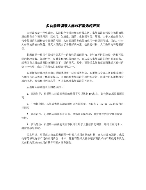
多功能可调谐太赫兹石墨烯超表面太赫兹波是一种电磁波,其波长介于微波和红外线之间。
太赫兹波在频段上独特的性质使其在多个领域得到广泛应用,如成像、通信、生物医学等。
然而,由于太赫兹波在大气中传播的削弱和信号漏损的问题,太赫兹通信和成像的应用一直受到限制。
因此,针对太赫兹波传输的问题,研究人员提出了各种解决方案,包括超材料、人工微结构和超表面等。
超表面是一种具有类似于等离子体的特性的表面结构,能够在不同的波段中进行可控制的物理参数,如透射率、反射率和相位等的调控。
自从发现太赫兹波的应用前景以来,超表面在太赫兹波调控方面得到了广泛的研究。
其中,石墨烯太赫兹超表面凭借其独特的热与电性质,成为了当前热门的研究领域之一。
石墨烯太赫兹超表面由石墨烯薄膜和一层金属等组成。
石墨烯与金属之间的电流耦合作用可以形成等离子体共振模式,进而影响太赫兹波的透射和反射。
通过控制石墨烯和金属的厚度、形状和排列方式等,可以实现对太赫兹波的可调控。
石墨烯太赫兹超表面的特点如下:1. 高透射率:石墨烯太赫兹超表面的透射率可以达到60%以上,比传统金属超表面更高。
2. 广调控范围:石墨烯太赫兹超表面可调控范围宽,可以在5 THz-30 THz波段内进行调控。
3. 高稳定性:石墨烯太赫兹超表面由石墨烯和金属组成,具有良好的稳定性和抗腐蚀性。
4. 多功能性:石墨烯太赫兹超表面不仅可以用于太赫兹波的调控,还可以应用于太赫兹传感等领域。
综上所述,石墨烯太赫兹超表面是一种极具应用前景的材料,在太赫兹波通讯、成像、传感等领域有着广泛的应用价值。
未来,随着石墨烯太赫兹超表面技术的不断改进和优化,其在相关领域的应用前景将不断扩展和深化。
多功能可调谐太赫兹石墨烯超表面
多功能可调谐太赫兹石墨烯超表面石墨烯是一种新颖的二维材料,由碳原子单层构成,具有出色的导电性、热导性和机械性能。
这些独特的特性使得石墨烯在多个领域具有广泛的应用前景,包括电子学、光学、传感器和能源存储等方面。
近年来,研究人员发现,通过对石墨烯进行微观结构设计和控制,可以创造出一种名为太赫兹石墨烯超表面的新型材料,具有多功能可调谐的特性,展现出了巨大的研究和应用潜力。
太赫兹波段是指电磁波频率介于红外光和微波之间的一段频段,具有很多在生物医学、通信、安全检测以及图像处理等方面的应用价值。
太赫兹波段的研究和应用一直受限于传统材料的特性,而石墨烯超表面的出现为太赫兹技术的进一步发展提供了新的可能性。
太赫兹石墨烯超表面是一种由石墨烯和微结构纳米天线构成的复合材料,其特性主要由石墨烯基板的电学和磁学响应以及微结构的尺寸和几何形状共同决定。
这种材料不仅能够实现太赫兹波段的调谐和调制,还具有光学透过率高、表面等离振荡增强、极化控制等特性。
多功能可调谐是太赫兹石墨烯超表面的重要特点之一。
对于太赫兹波段的调制和控制,传统的材料和结构存在一定的局限性,而太赫兹石墨烯超表面通过调控石墨烯基板的电学和磁学性质,可以灵活地调谐太赫兹波段的传输特性。
研究表明,通过改变石墨烯基板的电化学氧化还原反应,可以调节石墨烯的电导率和介电常数,从而实现太赫兹波段的频率调谐和相位调制。
太赫兹石墨烯超表面的微结构设计也可以通过控制微结构的尺寸和排列方式,实现太赫兹波段的色散调节和波束操控。
这种多功能可调谐的特性使得太赫兹石墨烯超表面在太赫兹技术和设备中具有广泛的应用前景,可以应用于太赫兹成像、传感、无线通信和天线技术等领域。
太赫兹石墨烯超表面也面临着一些挑战和问题。
目前太赫兹石墨烯超表面的制备和加工工艺尚不够成熟,导致材料的稳定性和可靠性有待提高。
太赫兹石墨烯超表面的多功能调谐机制和光学性能还需要深入研究和理解,才能实现更加精确和可控的太赫兹波调制和控制。
拓扑柔凝胶 中科海势

拓扑柔凝胶中科海势English Answer:Topological organogels are a class of soft materials that are composed of a network of cross-linked polymer chains that form a continuous phase and a dispersed phase of organic molecules. The topology of the polymer network determines the physical properties of the organogel, such as its stiffness, strength, and toughness.Topological organogels have been used in a variety of applications, including drug delivery, tissue engineering, and sensors. In drug delivery, topological organogels can be used to encapsulate and release drugs in a controlled manner. In tissue engineering, topological organogels can be used to create scaffolds for cell growth. In sensors, topological organogels can be used to detect the presence of specific molecules or ions.Topological organogels are a promising class ofmaterials with a wide range of potential applications. As research into these materials continues, new applicationsfor topological organogels are likely to be discovered.中文回答:拓扑柔凝胶是由交联聚合物链网络形成连续相和有机分子分散相组成的软材料。
211233502_阿秒时间抖动的全保偏掺铒光纤激光器
阿秒时间抖动的全保偏掺铒光纤激光器赵洺贺1,2,杨若傲2,陈子扬2,王爱民2,李倩1,张志刚2*(1.北京大学信息工程学院,广东深圳 518055;2.北京大学电子学院区域光纤通信网和新型光通信系统国家重点实验室,北京 100871)摘要:近年来,超稳光生微波和远距离时频同步等高精度、高速科学研究对低噪声飞秒光纤激光器具有迫切的需求。
为实现低时间抖动噪声的激光种子源,基于“光积木”结构,设计并搭建了一台重复频率为100 MHz的全保偏掺铒锁模光纤激光器,“光积木”结构可以有效地抑制激光器的机械噪声和重频漂移。
采用平衡光学互相关技术,首次从全保偏锁模光纤激光器的出射脉冲中直接进行了高精度的时间抖动测量。
该激光器在傅里叶频率10 kHz至1 MHz的积分区间内,积分均方根时间抖动仅为98.36 as。
关键词:飞秒激光器;时间抖动;平衡光学互相关中图分类号:TB939 文献标志码:A 文章编号:1674-5795(2023)03-0144-05All⁃PM Er: fiber laser with attosecond timing jitterZHAO Minghe1,2, YANG Ruo'ao2, CHEN Ziyang2, WANG Aimin2, LI Qian1, ZHANG Zhigang2*(1. School of Electronic and Computer Engineering, Peking University, Shenzhen, 518055, China;2. State Key Laboratory of Advanced Optical Communication Systems and Networks,School of Electronics, Peking University, Beijing 100871, China)Abstract: In recent years, low⁃noise femtosecond fiber lasers are widely demanded in high⁃precision and high⁃speed research such as ultra⁃stable photogenerated microwave and long⁃distance time⁃frequency transfer. To realize a laser seed with low⁃timing⁃jitter noise, an 100 MHz all⁃polarization⁃maintaining mode⁃locked Er:fiber laser was demonstrated on "optical cube". The"optical cube" configuration can effectively suppress the mechanical noise and the drift of the repetition rate. Based on the balanced optical cross⁃correlator technique, this is the first time to per⁃form high⁃precision time jitter measurement of the pulse train directly from an all polarization⁃maintaining mode⁃locked Er:fiber laser. The integrated root⁃mean⁃square timing jitter from 10 kHz to 1 MHz offset frequency is only 98.36 as.Key words: femtosecond laser; timing jitter; balanced optical cross⁃correlator0 引言近年来,低噪声的被动锁模激光器在超远距离时间同步[1]和超稳光生微波[2-3]等高精度科学实验中发挥了重要的作用。
- 1、下载文档前请自行甄别文档内容的完整性,平台不提供额外的编辑、内容补充、找答案等附加服务。
- 2、"仅部分预览"的文档,不可在线预览部分如存在完整性等问题,可反馈申请退款(可完整预览的文档不适用该条件!)。
- 3、如文档侵犯您的权益,请联系客服反馈,我们会尽快为您处理(人工客服工作时间:9:00-18:30)。
PUBLISHED ONLINE: 29 MAY 2011 | DOI: 10.1038/NPHOTON.2011.102
Broadband graБайду номын сангаасhene polarizer
Qiaoliang Bao1, Han Zhang2,5, Bing Wang3, Zhenhua Ni4, Candy Haley Yi Xuan Lim1, Yu Wang1, Ding Yuan Tang2 and Kian Ping Loh1 *
Conventional polarizers can be classified into three main modes of operation: sheet polarizer using anisotropic absorption media, prism polarizer by refraction and Brewster-angle polarizer by reflection1. These polarizing components are not easily integrated with photonic circuits. The in-line fibre polarizer, which relies on polarization-selective coupling between the evanescent field and birefringent crystal2 or metal3–7, is a promising alternative because of its compatibility with most fibre-optic systems. Here, we demonstrate the operation of a broadband fibre polarizer based on graphene, an ultrathin two-dimensional carbon material. The out-coupled light in the telecommunication band shows a strong s-polarization effect with an extinction ratio of 27 dB. Unlike polarizers made from thin metal film, a graphene polarizer can support transverseelectric-mode surface wave propagation due to its linear dispersion of Dirac electrons. Graphene has attracted a high level of research interest because of its exceptional electronic transport properties8, which have great potential in applications in the field of nanoelectronics. Its photonic properties are equally remarkable9,10. The universal optical conductance of graphene is defined by the fine structure constant and is independent of frequency over a wide range11. Its zero bandgap affords the benefit of high-bandwidth detection of light12. The facile saturation of its absorption due to Pauli blocking enables graphene to be used as a saturable absorber in broadband, ultrafast mode-locked lasers for use in telecommunications13,14. Its twodimensional nature also allows the fabrication of photonic circuits with ultrathin optical elements. In these circuits, graphene may be used to carry out the creation, routing, modulation or detection of light. Light modulation by means of polarization management is vital to avoid signal fading and error in coherent optic communications as well as in optical gyroscopes and interferometric sensors. The ability to couple and modulate light with such an ultrathin guiding material has yet to be experimentally demonstrated despite several theoretical investigations15–19. In this Letter, we demonstrate the coupling, guiding and polarizing of electromagnetic waves by graphene. The polarization mechanism is attributed to the differential attenuation of two polarization modes. In conventional two-dimensional electron systems, for example consisting of an ultrathin metal film and a GaAs/AlGaAs quantum well, the local dynamic conductivity described by the Drude model has the form s(v) ¼ inse 2/m(v þ it) (ref. 20), where ns , e, m and t are the concentration, charge, effective mass and scattering rate of two-dimensional electrons, respectively. As s(v) has a positive imaginary part s′′ , only the transversemagnetic (TM) mode can propagate in such structures; the transverseelectric (TE) mode is forbidden at a single interface between a metal and a dielectric according to boundary conditions19. The spectra of electromagnetic modes are sensitive to the electron (hole) mass. However, the situation in graphene is quite different because of its massless Dirac fermions. The dynamic conductivity of graphene can be determined from the Kubo formalism, consisting of intraband and interband contributions: s(v) ¼ sintra(v) þ sinter(v) (see Methods)21,22. The imaginary part s′′ plays an important role in the propagation of surface waves in a graphene sheet. The imaginary part of sintra(v) is always positive so that the TM mode can be supported (providing the chemical potential m = 0). At Év/2 . |m|, the contribution of interband optical transition gives rise to the negative imaginary part of sinter(v), which supports the conditions for TE mode existence19. This TE mode has a weakly damped wave propagating along the graphene sheet at close to the velocity of light19, and it is this that underpins the basis for the development of a broadband graphene TE-pass polarizer. Figure 1a presents a schematic of an in-line fibre-to-graphene coupler, capable of coupling electromagnetic waves into a twodimensional graphene plane. Optical images of the graphene optical device are shown in Fig. 1b,c. In this configuration, the dispersion and birefringence (the effective index difference) of the planar waveguide play important roles in the effective coupling of light and the selectivity for wavelength and polarization. Similar to surface plasmon polaritons (SPP) in metal films23, radiation originating from leaky modes or surface scattering are key signatures of strong perturbations of the fundamental core mode by graphene in terms of coupling and guiding. The radiative green light (Fig. 1d) that originates from the interaction of the graphene and fibre can be observed easily with the naked eye, indicating effective coupling. Such leakage radiation shows distance-dependent damping (Supplementary Fig. S2c). With the help of a polarization analyser equipped with an optical microscope (Supplementary Fig. S2), it was found that the radiative light is highly s-polarized (orthogonal to the plane of incidence), which attests to coupling and guiding of the TE mode by the graphene. This polarizing effect is highly reproducible when white light is used as the excitation source (Supplementary Fig. S3), suggesting the possibility of broadband polarization of light. The polarization extinction ratios at both visible and near-infrared (NIR) frequencies were measured (see Methods and Supplementary Information). Using visible light as the excitation source (Supplementary Fig. S4), monolayer graphene with propagation distance LG ¼ 2.1 mm gave an extinction ratio of 14.2 dB for green (532 nm) light and 13.9 dB for blue (488 nm) light, as shown in Fig. 2a. The maximum output occurred at u ¼ 08, and the minimum appeared at u ¼ 908, confirming the s-polarized nature of transmitted light. Even stronger polarization occurred for NIR wavelengths, with an extinction ratio of 18.3 dB at 980 nm, 15.7 dB at 1,300 nm, 18.4 dB at 1,480 nm