AUO KD101N2-40NA-A1国显10.1寸TFT规格书
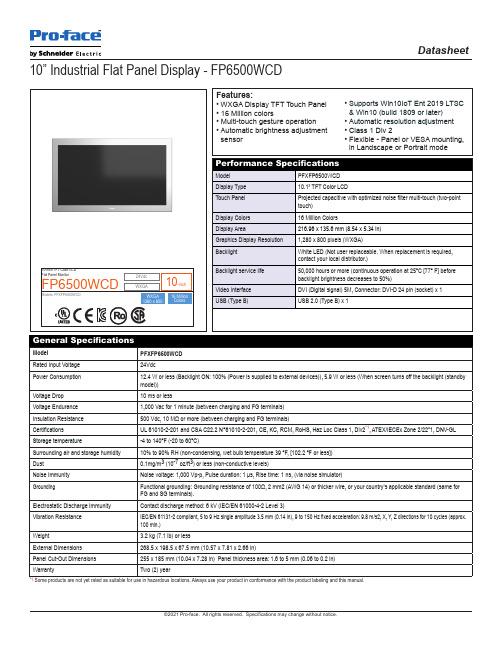
Pro-face 10英寸TFT彩色LCD平面显示器FP6500WCD说明书
©2021 Pro-face. All rights reserved. Specifications may change without notice.
FP6500WCD - External Dimensions FP6500WCD - Cut-Out Dimensions
Datasheet
Electrostatic Discharge Immunity
Contact discharge method: 6 kV (IEC/EN 61000-4-2 Level 3)
Vibration Resistance
IEC/EN 61131-2 compliant, 5 to 9 Hz single amplitude 3.5 mm (0.14 in), 9 to 150 Hz fixed acceleration: 9.8 m/s2, X, Y, Z directions for 10 cycles (approx. 100 min.)
USB (Type B)
USB 2.0 (Type B) x 1
General Specifications
Model
PFXFP6500WCD
Rated Input Voltage
24Vdc
Power Consumption
12.4 W or less (Backlight ON: 100% (Power is supplied to external devices)), 5.9 W or less (When screen turns off the backlight (standby model))
Features: • WXGA Display TFT Touch Panel • 16 Million colors • Multi-touch gesture operation • Automatic brightness adjustment
AUO 10.1寸玻璃规格书(2015.1.5)

1 Li-Hsin Rd. 2. Science-Based Industrial ParkHsinchu 300, Taiwan, R.O.C.Tel: +886-3-500-8899Fas: +886-3-577-2730n ti a lF o r FO n 2014/08Doc. version : 1.1Total pages : 13Date :2014/05/13Note:The content of this specification is subject to change.© 2013 AU Optronics All Rights Reserved, Do Not Copy.n ti a lF o r FO R 8Record of Revisionn ti a lF o r Fn 2014/08ContentsA.General Information.....................................................................................................................................3B.Outline Dimension .......................................................................................................................................41. LCD Outline.................................................................................................................................................4C.Electrical Specifications..............................................................................................................................51. LCD Pin Assignment (FPC bonding side)...................................................................................................52. Electrical DC Characteristics.. (6)3. Compatible Driver IC...................................................................................................................................6D.Optical Specification....................................................................................................................................7E.Reliability Test Items....................................................................................................................................8F.Packing and Marking...................................................................................................................................91. Packing Form ..............................................................................................................................................9G.Mark information........................................................................................................................................101. Chip Alignment Mark for Polarizer Attachment, COG and FPC Bonding . (10)H.Precautions (12)Appendix A: (13)n ti a lF o r FO R C H IN AMA RK E T US EON L YI nt er na lU se On l y O n 2014/08A.General InformationThis product is only cell.n ti a lF o r Fn 2014/08B.Outline Dimension1. LCD Outlinen ti a lF o r FO R C H IN AMA RK E T US EON L YI nt er na lU se On l y O n 2014/08C.Electrical Specifications1168n ti a lF o r FO R C H IN AM2014/082. Electrical DC Characteristicsn ti a lF o r Fn 2014/08D.Optical SpecificationNote 3. Measured at the center area of the panel when all the input terminals of LCD panel are electrically opened.n ti a lF o r FO 14/08n ti a lF o r FO 2014/08F.Packing and Marking1. Packing Formn ti a lF o r FO R C H IN AMA RK E T US EON L YI nt er na lU se On l y O n 2014/08G.Mark information1. Chip Alignment Mark for Polarizer Attachment, COG and FPC Bondingn ti a lF o r FO R C H IN AMA RK E T US EON L YI nt er na lU se On l y O n 2014/08Unit:umn ti a lF o r FO R C H IN AMA RK E T US EON L YI nt er na lU se On l y O n 2014/08H.Precautions1.Do not twist or bend the module and prevent the unsuitable external force for display module duringassembly.2.Adopt measures for good heat radiation. Be sure to use the module with in the specified temperature.3.Avoid dust or oil mist during assembly.4.Follow the correct power sequence while operating. Do not apply the invalid signal, otherwise, it will causeimproper shut down and damage the module.5.Less EMI: it will be more safety and less noise.6.Please operate module in suitable temperature. The response time & brightness will drift by differenttemperature.7.Avoid to display the fixed pattern (exclude the white pattern) in a long period, otherwise, it will cause imagesticking.8.Be sure to turn off the power when connecting or disconnecting the circuit.9.Polarizer scratches easily, please handle it carefully.10.Display surface never likes dirt or stains.11.A dewdrop may lead to destruction. Please wipe off any moisture before using module.12.Sudden temperature changes cause condensation, and it will cause polarizer damaged.13.High temperature and humidity may degrade performance. Please do not expose the module to thedirect sunlight and so on.14.Acetic acid or chlorine compounds are not friends with TFT display module.15.Static electricity will damage the module, please do not touch the module without any grounded device.16.Do not disassemble and reassemble the module by self.17.Be careful do not touch the rear side directly.18.No strong vibration or shock. It will cause module broken.19.Storage the modules in suitable environment with regular packing.20.Be careful of injury from a broken display module.21.Please avoid the pressure adding to the surface (front or rear side) of modules, because it will cause thedisplay non-uniformity or other function issue.n ti a lF o r FO R C H IN AMA RK E T US EON L YI nt er na lU se On l y O n 2014/08Appendix A:A.1 Pixel Format ImageFollowing figure shows the relationship of the input signals and LCD pixel format.n ti a lF o r FO R C H IN AMA RK E T US EON L YI nt er na lU se On l y O n 2014/08。
Riverdi 10.1 寸 TFT 显示屏数据手册说明书

ITEM CONTENTS UNIT LCD Type TFT/Transmissive/Normally Black/IPS / Size 10.1 Inch Viewing Direction Free / Outside Dimensions (W x H x D) 246.66 x 151.30 x 13.48 mm Active Area (W x H) 216.96 x 135.60 mm Pixel Pitch (W x H) 0.1695 x 0.1695 mm Resolution 1280 x 800 / Brightness 1000 cd/m 2 Color Depth 16.7 M / Pixel Arrangement RGB Vertical Stripe / Driver IC of Board STM32H747XIH6 / External SDRAM 64Mbit (32-bit access) / External Flash Memory 512Mbit / Supply Voltage for Module 6.0-36.0 V With/Without Touch Without Touch Panel / Weight 615 g STM32 EMBEDDED 10.1" DISPLAY DATASHEET RVT101HVSFWN00 Rev.1.1 2022-02-14 F T M O D U L E S P E C I F I C A T I O N Note 1: RoHS3 compliant Note 2: LCM weight tolerance: ± 5%.REVISION RECORDREV NO. REV DATE CONTENTS REMARKS1.0 2022-01-10 Initial release1.1 2022-02-14 Update the absolute maximum ratingof V to 0V-48.0VCONTENTSREVISION RECORD (2)CONTENTS (3)MODULE CLASSIFICATION INFORMATION (4)ASSEMBLY GUIDE (5)MODULE DRAWING (6)ABSOLUTE MAXIMUM RATINGS (7)ELECTRICAL CHARACTERISTICS (7)BACKLIGHT ELECTRICAL CHARACTERISTICS (7)ELECTRO-OPTICAL CHARACTERISTICS (8)BOARD INTERFACES AND CONNECTORS (10)USER INTERFACES (16)DISPLAY SEPCIFICATION (18)INSPECTION (18)RELIABILITY TEST (20)LEGAL INFORMATION (21)MODULE CLASSIFICATION INFORMATIONRV T 101 H V S F W N 00 1. 2. 3. 4. 5. 6. 7. 8. 9. 10.ASSEMBLY GUIDEMounting frameFor dimensions 3.5”, 4.3”, 5.0”, 7.0” and 10.1”, the product with mounting frame version is available. Thanks to the four catches attached to the side, frame provides strong assembly to the surface by mounting element (like the screw, see Figure 1). The frames are specially designed to fit Riverdi products perfectly. The diameter of the mounting hole is 3.5mm.Figure 1. Mounting frameABSOLUTE MAXIMUM RATINGSPARAMETER SYMBOL MIN MAX UNIT NOTESupply Voltage for Module VDD 0 48.0V Note 1Digital I/O signals Voltage - -0.5 3.3 Note 1, 2Operating Temperature T OP-20 70 °CStorage Temperature T ST-30 80 °CStorage Humidity (@ 25 ± 5°C) H ST10 - % RHOperating Ambient Humidity (@ 25 ± 5°C) H OP10 - % RHNote 1. Exceeding maximum values may cause improper operation or permanent damageto the unit.Note 2. Most of the GPIOs have the 5.0 V tolerant input voltage, please refer to the datasheetof STM32H747XIH6 for more details.ELECTRICAL CHARACTERISTICSPARAMETER SYMBOL MIN TYP MAX UNIT Supply Voltage for Module VDD_IN 6.0 12.0 36.0 VPOWER‘ENABLE’ = ‘0’***************************I VDD_IN=6.0 V-60 -uA ****************************I VDD_IN=12.0 V-147 -uA ****************************I VDD_IN=24.0 V-388 -uA ****************************I VDD_IN=36.0 V-629 -uAPOWER‘ENABLE’ = ‘1’***************************I VDD_IN=6.0 V - 851 - mA ****************************I VDD_IN=12.0 V- 412 - mA ****************************I VDD_IN=24.0 V- 226 - mA ****************************I VDD_IN=36.0 V- 160 - mAInput Voltage “H” Level V IH 2.0 - 3.3 V Input Voltage “L” Level V IL 0 - 0.8 V Note. POWER ‘ENABLE’ refers to pin 3, ‘ENABLE’ of the power input connector.By default, POWER ‘ENABLE’ = ‘1’,When POWER ‘ENABLE’ = ‘0’, the device is turned off.BACKLIGHT ELECTRICAL CHARACTERISTICSPARAMETER SYMBOL MIN TYP MAX UNIT NOTE Lifetime - - 50,000 - hours NOTE 1Note 1. Operating life means the period in which the LED brightness goes down to 50% ofthe initial brightness. Typical operating lifetime is the estimated parameter.ELECTRO-OPTICAL CHARACTERISTICSITEM SYMBOL CONDITION MIN TYP MAX UNIT RMK NOTEResponse Time Tr+Tfθ=0°∅=0° - 25 35 ms FIG 2. 4Contrast Ratio Cr 800 1000 - --- FIG 3. 1 Luminance δ- 75 - % FIG 3. 3 Figure 3.Contrast Ratio =Average Surface Luminance with all white pixels (P1,P2,P3,P4,P5) Average Surface Luminance with all black pixels (P1,P2,P3,P4,P5)Note 2.Surface luminance is the LCD surface from the surface with all pixels displaying white. For more information see Figure 3.Lv = Average Surface Luminance with all white pixels (P1, P2, P3, P4, P5)Note 3.The uniformity in surface luminance δWHITE is determined by measuring luminance at each test position 1 through 5, and then dividing the minimum luminance of 5 points luminance by maximum luminance of 5 points luminance. For more information see Figure 3.δ WHITE =Minimum Surface Luminance with all white pixels (P1,P2,P3,P4,P5) Maximum Surface Luminance with all white pixels (P1,P2,P3,P4,P5)Note 4. Response time is the time required for the display to transition from white to black (Rise Time, Tr) and from black to white (Decay Time, Tf). For additional information see Figure 2. The test equipment is Autronic-Melchers’s ConoScope series.Note 5. CIE (x, y) chromaticity, the x, y value is determined by measuring luminance at each test position 1 through 5, and then calculating the average value.Note 6. Viewing angle is the angle at which the contrast ratio is greater than 2. For TFT module the contrast ratio is greater than 10. The angles are determined for the horizontal or x axis and the vertical or y axis with respect to the z axis which is normal to LCD surface. For more information see Figure 4.Note 7. For viewing angle and response time testing, the testing data is based on Autronic-Melchers’s ConoScope series. Instruments for Contrast Ratio, Surface Luminance, Luminance Uniformity, CIE the test data is based on TOPCON’s BM-5 photo detector.Figure 2. The definition of response timeFigure 3. Measuring method for Contrast ratio, surface luminance, Luminance uniformity, CIE (x, y) chromaticityA: 5mmB: 5mmH, V: Active AreaLight spot size ∅=5mm, 500mm distancefrom the LCD surface to detector lens.Measurement instrument is TOPCON’Sluminance meter BM-5Figure 4. The definition of viewing angleBOARD INTERFACES AND CONNECTORSPower input connectorThe 1.25mm, 5-pin Molex connector labeled as “POWER’ is power input connector.There is an internal reverse polarity protection which ensures that the device is not damaged if the power supply polarity is reversed.NO. PIN DESCRIPTION NOTE1 VDD_IN Power supply input; 6.0-36.0VNote 12 VDD_IN Power supply input; 6.0-36.0V3 ENABLE Enable/ Disable power supply. Note 24 GND Ground5 GND GroundNote 1: STM32 Embedded Display allows to directly connect one additional display to the system. There is RiBUS connector on the board where you can connect any of intelligent display from Riverdi based on EVE4 (BT817Q). However, please note that it may change power supply requirement as below:The power supply voltage must range from 7.0V- 14.0 V (TYP. 9V), if Riverdi EVE4 10.1” series display is connected through RiBUS. At the same time, please also configure the backlight voltage jumpers, P5 and P12, according to subchapter 10.8, note 1.The power supply voltage ranges from 6.0 V- 36.0V if any of Riverdi EVE4 3.5”,4.3”,5.0” and 7.0” series display is connected through RiBUS. At the same time, please also configurethe backlight voltage jumpers, P5 and P12, according to subchapter 10.8, note 1.Note 2: By default, pin “ENABLE” is pull up to VDD and enabled. To disable, ground the pin to turn off the device completely.USB interfaceThe 1.25mm, 5-pin Molex connector labeled as “USB’ is USB interface.NO. PIN DESCRIPTION NOTE1 VCC_USB Power supply Note 12 D- USB data-3 D+ USB data+4 ID USB OTG ID; Host /Device detect Note 15 GND GroundNote 1. Configuration of the USB Host/Device mode:Host Mode: Pin 4 (ID) should be connected to GND.In this mode, it can provide +5V output voltage to the connected USB device and Max output current 500 mA.Device Mode: Pin 4 (ID) should be not connected (floating).RS485 interfaceThe 1.25mm, 4-pin Molex connector labeled as “RS485’ is RS485 interface.NO. PIN DESCRIPTION NOTE1 A Non-inverting receiver input and non-inverting driver output2 B Inverting receiver input and inverting driver output3 GND Ground4 VDD_IN Power supply input; 6.0-36.0VRS232 interfaceThe 1.25mm, 5-pin Molex connector labeled as “RS232’ is RS232 interface.NO. PIN DESCRIPTION NOTE1 RTS Request to send2 CTS Clear to send3 TXD Transmit Data4 RXD Receive Data5 GND Ground2 x CAN FD interfacesThe main board supports 2 channels of the CANFD (Control Area Network Flexible Data-Rate) communication bus, based on the high-speed (2.5-8.0Mbps) CAN transceiver.2 pcs of 1.25mm, 4-pin Molex connectors labeled as “CAN1’ and “CAN2” are r espectively interfaces of CAN FD1 and CAN FD2.NO. PIN DESCRIPTION NOTE1 GND Ground2 CAN_L CAN Low-Level Voltage3 CAN_H CAN High-Level Voltage4 VDD_IN Power supply input; 6.0 – 36.0 VHaptic feedback connectorThe 1.25mm, 2-pin Molex connector labeled as “HAPTIC’ is haptic feedback connector. Haptic feedback P7 is used to connect with the haptic motor directly.NO. PIN DESCRIPTION NOTE1 OUT+ Positive haptic driver differential outputNote 12 OUT_ Negative haptic driver differential outputNote 1: The haptic driver applies DRV2605L and is controlled by internal I2C1.SWD (Serial Wire Debug) connectorThe 1.25mm, 6-pin Molex connector labeled as “SWD” is SWD interface, which is used for programing the MCU on board.NO. PIN DESCRIPTION NOTE1 VCC_+3.3V Power input2 SW_CLK Serial wire clock3 GND Ground4 SW_DIO Serial wire debug data input/output5 RST Reset; Active low6 SWO Serial wire trace outputRiBUSAny size of the Riverdi EVE4 series display can be connected through RiBUS to act as a slave module to the mainboard.NO. PIN DESCRIPTION NOTE1 VCC_+3.3V Supply voltage for module; TYP3.3Vfrom 7.0 - 14.0V (TYP. 9V).For Riverdi EVE4 series display ranging from sizes of 3.5” to 7.0”,the backlight voltage (BLVDD) is 5V.Backlight jumper selectors, P5 and P12, labeled as “BLVDD SEL” are used to configure the backlight voltage range.Warning! When you configure the jumpers, be sure that the module is powered off.DO NOT change ANY jumpers while the module has power. Improper operation might cause permanent damage to the unit.Please also pay special attention to not misplace the jumpers. Incorrect jumpers setting may lead to damage to the module as well.Table 2. Backlight power (7.0V-14.0V) select jumpers settingExpansion connectorThe main board has one 1.27mm, 40-pin expansion pin header which is labeled as “EXPANSION CONNECTOR’,It provides direct access to below GPIOs of MCU STM32H747XIH6,which make it possible to easily extend a daughterboard for a specific application.• 2 x I2C• 1 x UART• 1 x USART• 1 x SPI• 1 x USB•7 x PWMs• 2 x DACs (Digital-to-analog)• 2 x ADCs (Analog-to-digital)Each of the GPIO pins can be configured by software as output (push-pull or open-drain, with or without pull-up or pull-down), as input (floating, with or without pull-up or pull-down) or as peripheral alternate function. Most of the GPIO pins are shared with digital or analog alternate functions. Please refer to the datasheet of MCU STM32H747XIH6 for more details.I/O PD13 15 16 PA3 I/OP GND 17 18 GND PI/O PC2 19 20 PA0_C I/OI/O PC3 21 22 PA1_C I/OI/O PA12 23 24 PC2_C I/OI/O PA9 25 26 PC3_C I/OI/O PA10 27 28 GND PI/O PJ8 29 30 PC13 I/OI/O P18 31 32 PA8 I/OI/O PJ10 33 34 PB11 I/OI/O PB0 35 36 PH4 I/OI/O PC6 37 38 PB12 I/OI/O PB14 39 40 PB15 I/ONote. The total output current I VCC=5V from pin 1 and pin3 is maximum 1A.The total output current I VCC=3.3V from pin 2 and pin 4 is maximum 500mA.Micro SD slotThe mainboard is equipped with Micro-SD slot, which supports all types of Micro SD cards.2 x 20-pin, 1.27 mm pin sockets for POE Add-on BoardThe 2 x 20-pin, 1.27 mm, pin sockets, labeled as U9a and U9b, are used to connect the Riverdi POE Add-on Board.The Riverdi POE Add-on Board features 10/100M Ethernet Port with Power-Over-Ethernet enabled. It allows you to power the module through the Ethernet port.Note: The Riverdi POE Add-on Board is sold separately.USER INTERFACES3 x push buttonsPush button labeled as “RST” is used to “RESET” the module.Another 2 push buttons labeled as BTN1, BTN2 are for user’s development.•BTN1(S1) is connected to pin 37, PC6, of the expansion connector.•BTN2(S2) is connected to pin 35, PB0, of the expansion connector.By default, R57 and R58 are not mounted. Please solder 0402 0R resistor or short R57, R58 to enable the pushbuttons BTN1(S1), BTN2(S2).3 x LEDs1 x LED, labeled as ‘PWR LED’, emits green light when the modules is powered.1 x LED, labeled as ‘USB OVR’, emits red light when VCC_USB pin is shorted.1 x LED, labeled as ‘USR LED’, is for user’s development.•The ‘USR LED’ is connected to pin 33, PJ10, of the expansion connector.By default, the resistor R60, (1k ohms) is soldered. Please remove R60 to use GPIO channel PJ10.D ISPLAY SEPCIFICATIONTFT resolutionThe supported resolution of the display in this module is 1280*800.Full TFT specificationFor detailed information on the display, please refer to datasheet of displayRVT101HVLFWN00.I NSPECTIONStandard acceptance/rejection criteria for TFT moduleInspection conditionAmbient conditions:•Temperature: 25 ± 2°C•Humidity: (60 ± 10) %RH•Illumination: Single fluorescent lamp non-directive (300 to 700 lux) Viewing distance: 35 ± 5cm between inspector bare eye and LCD.Viewing Angle: U/D: 45°/45°, L/R: 45°/45°Inspection standardThe LCD TFT has zero bad pixels. Please refer the item “Bright/Dark dots”. ITEM CRITERIONBlack spots,white spots,light leakage,Foreign Particle(round Type)D=(x+y)/2Spots density: 10 mmSize =10.1”Average Diameter Qualified QtyD ≤ 0.2 mm Ignored0.2 mm < D ≤ 0.3 mm N≤40.5mm < D N = 0LCD black spots,white spots,light leakage(line Type)Spots density: 10 mmSize =10.1”Length WidthQualifiedQty - W ≤ 0.05Ignored L ≤ 5.00.05< W ≤ 0.1N ≤ 3 5.0 < L0.10< W5.0 < LN = 0Bright/Dark DotsSize =10.1”Item Qualified Qty Bright dots 0Dark dots 0 Cluster Bright Dots or Dark Dots 0 Total Bright and Dark Dots 0Clear spotsSize ≥ 5”Average Diameter Qualified QtyD < 0.2 mm Ignored0.2 mm < D < 0.3 mm 40.3 mm < D < 0.5 mm 20.5 mm < D 0 Spots density: 10 mmTouch panel spotSize ≥ 5"Average Diameter Qualified QtyD < 0.25 mm Ignored0.25 mm < D < 0.5 mm 40.5 mm < D 0Touch panel White line ScratchSize ≥ 5"Length Width Qualified Qty - W < 0.03 IgnoredL < 5.0 0.03 < W < 0.05 2- 0.05 < W 0RELIABILITY TESTNO.TEST ITEMTEST CONDITIONNOTE1 High Temperature Storage 80°C/120 hoursNote 12 Low Temperature Storage -30°C/120 hours3 High Temperature Operating 70 °C /120 hours Note 2. Before cosmetic and function test, the product must have enough recovery time, at least 2 hours at room temperature.© 2022 Riverdi Page 21 of 21 RVT101HVSFWN00L EGAL INFORMATIONRiverdi grants the guarantee for the proper operation of the goods for a period of 12 months from the date of possession of the goods. If in a consequence of this guaranteed execution the customer has received the defects-free item as replacement for the defective item, the effectiveness period of this guarantee shall start anew from the moment the customer receives the defects-free item.Information about device is the property of Riverdi and may be the subject of patents pending or granted. It is not allowed to copy or disclosed this document without prior written permission.Riverdi endeavors to ensure that all contained information in this document is correct but does not accept liability for any error or omission. Riverdi products are in developing process and published information may be not up to date. Riverdi reserves the right to update and makes changes to Specifications or written material without prior notice at any time. It is important to check the current position with Riverdi.Images and graphics used in this document are only for illustrative the purpose. All images and graphics are possible to be displayed on the range products of Riverdi, however the quality may vary. Riverdi is no liable to the buyer or to any third party for any indirect, incidental, special, consequential, punitive, or exemplary damages (including without limitation lost profits, lost savings, or loss of business opportunity) relating to any product, service provided or to be provided by Riverdi, or the use or inability to use the same, even if Riverdi has been advised of the possibility of such damages.Riverdi products are not fault tolerant nor designed, manufactured or intended for use or resale as on line control equipment in hazardous environments requiring fail –safe performance, such as in the operation of nuclear facilities, aircraft navigation or communication systems, air traffic control, direct life support machines or weapons systems in which the failure of the product could lead directly to death, personal injury or severe physical or environmental damage (‘High -Risk Activities’). Riverdi and i ts suppliers specifically disclaim any expressed or implied warranty of fitness for High-Risk Activities. Using Riverdi products and devices in 'High-Risk Activities' and in any other application is entirely at the buyer’s risk, and the buyer agrees to def end, indemnify, and hold harmless Riverdi from all damages, claims or expenses resulting from such use. No licenses are conveyed, implicitly or otherwise, under any Riverdi intellectual property rights.。
Simatic HMI Smart 1000 IE 10英寸宽屏TFT显示屏用户手册说明书
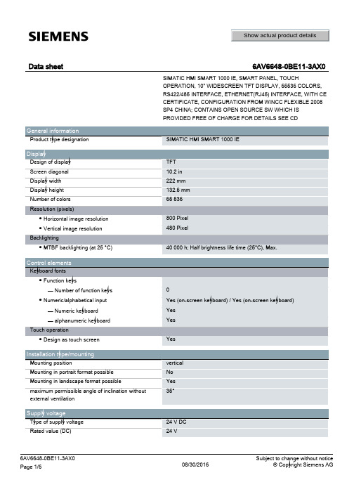
vertical No Yes 35°
24 V DC 24 V
6AV6648-0BE11-3AX0 Page 1/6
08/30/2016
Subject to change without notice © Copyright Siemens AG
permissible range, lower limit (DC) permissible range, upper limit (DC)
SIMATIC HMI SMART 1000 IE
TFT 10.2 in 222 mm 132.5 mm 65 536
800 Pixel 480 Pixel
40 000 h; Half brightness life time (25°C), Max.
0 Yes (on-screen keyboard) / Yes (on-screen keyboard) Yes Yes
Show actual product details
Data sheet
General information Product type designation
Display Design of display Screen diagonal Display width Display height Number of colors Resolution (pixels) ● Horizontal image resolution ● Vertical image resolution Backlighting ● MTBF backlighting (at 25 °C)
800 100 Yes Yes No Yes
100 Yes; No permanent window can be coLeabharlann figured Yes Yes Yes
友达10.4寸G104STN01.0液晶屏规格书-杭州旭虹科技

( V ) Preliminary Specifications( ) Final SpecificationsModule 10.4 Inch Color TFT-LCD Model Name G104STN01.0Customer Date Checked &Approved by Approved by DateGrace Hung 2013/08/16 Prepared byJohnson Lin 2013/08/16 General Display Business Division / AU Optronics corporationContents1. Operating Precautions (4)2. General Description (5)2.1 Display Characteristics (5)2.2 Optical Characteristics (6)3. Functional Block Diagram (9)4. Absolute Maximum Ratings (10)4.1 Absolute Ratings of TFT LCD Module (10)4.2 Absolute Ratings of Environment (10)5. Electrical Characteristics (11)5.1 TFT LCD Module (11)5.2 Backlight Unit (13)6. Signal Characteristics (14)6.1 Pixel Format Image (14)6.2 Scanning Direction (14)6.3 TFT-LCD Interface Signal Description (15)6.4 The Input Data Format (16)6.5 TFT-LCD Interface Timing (17)6.6 Power ON/OFF Sequence (18)7. Connector & Pin Assignment (19)7.1 TFT-LCD Signal (CN1): LVDS Connector (19)7.2 LED Backlight Unit (CN2): Driver Connector (19)7.3 LED Backlight Unit (CN4): Light bar Connector (19)8. Reliability Test Criteria (20)9. Mechanical Characteristics (21)9.1 LCM Outline Dimension (Front View) (21)9.2 LCM Outline Dimension (Rear View) (22)10. Label and Packaging (23)10.1 Shipping Label (on the rear side of TFT-LCD display) (23)10.2 Carton Package (23)11 Safety (25)11.1 Sharp Edge Requirements (25)11.2 Materials (25)11.3 Capacitors (25)11.4 National Test Lab Requirement (25)Record of RevisionVersion and Date Page Old description New Description1. Operating Precautions1) Since front polarizer is easily damaged, please be cautious and not to scratch it.2) Be sure to turn off power supply when inserting or disconnecting from input connector.3) Wipe off water drop immediately. Long contact with water may cause discoloration orspots.4) When the panel surface is soiled, wipe it with absorbent cotton or soft cloth.5) Since the panel is made of glass, it may be broken or cracked if dropped or bumped onhard surface.6) To avoid ESD (Electro Static Discharde) damage, be sure to ground yourself before handlingTFT-LCD Module.7) Do not open nor modify the module assembly.8) Do not press the reflector sheet at the back of the module to any direction.9) In case if a module has to be put back into the packing container slot after it was takenout from the container, do not press the center of the LED light bar edge. Instead, press at the far ends of the LED light bar edge softly. Otherwise the TFT Module may be damaged.10) At the insertion or removal of the Signal Interface Connector, be sure not to rotate nortilt the Interface Connector of the TFT Module.11) TFT-LCD Module is not allowed to be twisted & bent even force is added on module in a veryshort time. Please design your display product well to avoid external force applying to module by end-user directly.12) Small amount of materials without flammability grade are used in the TFT-LCD module. TheTFT-LCD module should be supplied by power complied with requirements of Limited Power Source (IEC60950 or UL1950), or be applied exemption.13) Severe temperature condition may result in different luminance, response time and lampignition voltage.14) Continuous operating TFT-LCD display under low temperature environment may acceleratelamp exhaustion and reduce luminance dramatically.15) The data on this specification sheet is applicable when LCD module is placed in landscapeposition.16) Continuous displaying fixed pattern may induce image sticking. It’s recommended to usescreen saver or shuffle content periodically if fixed pattern is displayed on the screen.2. General DescriptionThis specification applies to the Color Active Matrix Liquid Crystal Display G104STN01.0composed of a TFT-LCD display, a driver and power supply circuit, and a LED backlight system. The screen format is intended to support SVGA (800(H) x 600(V)) screen and 16.2M (RGB 8-bits) or 262k colors (RGB 6-bits).LED driving board for backlight unit is included in G104STN01.0 and the LED unit is replaceable. All input signals are LVDS interface and compatible with G104SN02 V2.G104STN01.0 designed with wide viewing angle; wide temperature and long life LED backlight is well suited for industial applications. G104STN01.0 is a RoHS product.2.1 Display CharacteristicsThe following items are characteristics summary on the table under 25 ℃ condition: ItemsUnitSpecifications Screen Diagonal [inch] 10.4Active Area [mm] 211.2 (H) x 158.4 (V) Pixels H x V 800 x 3(RGB) x 600 Pixel Pitch [mm] 0.264 x 0.264 Pixel Arrangement R.G.B. Vertical Stripe Display ModeTN, Normally White Nominal Input Voltage VDD [Volt] 3.3 (typ.) Typical Power Consumption [Watt] 2.88WAll black pattern Weight [Grams] 365(Typ.)Physical Size [mm] 243.0(H) x 184.0(V) x 6.5(D)(Typ.) Electrical Interface 1 channel LVDS Surface Treatment Anti-glare, Hardness 3H Support Color16.2M / 262K colors Temperature Range OperatingStorage (Non-Operating) [o C] [o C]-20 to +80 -20 to +80 RoHS ComplianceRoHS Compliance2.2 Optical CharacteristicsThe optical characteristics are measured under stable conditions at 25 (Room Temperature):℃Item Unit Conditions Min. Typ. Max. RemarkWhite Luminance[cd/m2] I F = 50mA/1 LED Line (center point) 300 400 -1 Uniformity % 5 Points 65 75 -2,3 Contrast Ratio500 700 - 4[msec]Rising - 10 20 [msec] Falling- 5 15 Response Time[msec] Raising + Falling - 15 35 5 [degree] [degree] Horizontal (Right) CR = 10 (Left) 70 70 80 80 - - Viewing Angle[degree] [degree]Vertical (Upper) CR = 10 (Lower) 50 60 60 70 - - 6 Red x - TBD - Red y - TBD - Green x- TBD - Green y - TBD - Blue x - TBD - Blue y - TBD - White x 0.28 0.31 0.34 Color / ChromaticityCoordinates (CIE 1931)White y0.30 0.33 0.36 Color Gamut%50-Note 1: Measurement method Equipment Pattern Generator, Power Supply, Digital Voltmeter, Luminance meter (SR_3 or equivalent) Aperture1with 50cm viewing distance ∘Test Point CenterEnvironment < 1 luxModule Driving EquipmentNote 2: Definition of 5 points position (Display active area: 211.2mm (H) x 158.4mm (V))Note 3: The luminance uniformity of 5 points is defined by dividing the minimum luminance values by the maximum test point luminanceNote 4: Definition of contrast ratio (CR):Note 5: Definition of response time:The output signals of photo detector are measured when the input signals are changed from “White” to “Black” (falling time) and from “Black” to “White” (rising time), respectively. The response time interval isNote 6: Definition of viewing angleViewing angle is the measurement of contrast ratio 10, at the screen center, over a 180° horizontal and ≧180° vertical range (off-normal viewing angles). The 180° viewing angle range is broken down as below: 90° (θ) horizontal left and right, and 90° (Φ) vertical high (up) and low (down). The measurement direction is typically perpendicular to the display surface with the screen rotated to its center to develop the desiredMinimum Brightness of five pointsδW9 = Maximum Brightness of five points Contrast ratio (CR)=Brightness on the “White” stateBrightness on the “Black” statemeasurement viewing angle.3. Functional Block DiagramThe following diagram shows the functional block of the 10.4 inch color TFT/LCD module:4. Absolute Maximum Ratings4.1 Absolute Ratings of TFT LCD ModuleItem Symbol Min Max Unit Logic/LCD Drive Voltage Vin -0.3 +4.0 [Volt]4.2 Absolute Ratings of EnvironmentItem Symbol Min Max Unit Operating Temperature TOP -20 +80 [o C] Operation Humidity HOP 5 95 [%RH] Storage Temperature TST -20 +80 [o C] Storage Humidity HST 5 95 [%RH] Note: Maximum Wet-Bulb should be 39℃ and no condensation.5. Electrical Characteristics 5.1 TFT LCD Module5.1.1 Power SpecificationSymbol Parameter Min Typ Max Units RemarkVDD Logic/LCD Input Voltage 3.0 3.3 3.6 [Volt]I VDD LCD Input Current - 320 - [mA]VDD=3.3V at 60 HZ, all Black PatternP VDD LCD Power comsumption - - 1.5 [Watt] VDD=3.3V at 60 HZ, all Black Pattern I rush LCDLCD Inrush Current-1.06-[A] Note 1; VDD=3.3VBlack Pattern, Rising time=470usVDD rpAllowable Logic/LCDDrive Ripple Voltage- -100 [mV] p-pVDD=3.3V at 60 HZ, all Black PatternNote 1: Measurement condition:VDD rising time0V3.3V5.1.2 Signal Electrical CharacteristicsInput signals shall be low or Hi-Z state when VDD is off.Note: LVDS Signal Waveform.Symbol ItemMin. Typ.Max. Unit RemarkVTH Differential Input High Threshold - - 100 [mV] VCM=1.2V VTL Differential Input Low Threshold 100 - - [mV] VCM=1.2V |VID |Input Differential Voltage100 400 600 [mV] VICMDifferential Input Common Mode Voltage1.1251.251.375[V]VTH/VTL=+-100mV5.2 Backlight Unit5.2.1 Parameter guideline for LED backlightFollowing characteristics are measured under a stable condition using a inverter at 25℃. (Room Temperature): Symbol Parameter Min.Typ.Max.Unit RemarkVCC Input Voltage 10.8 12 12.6 [Volt]I VCC Input Current - 0.32 - [A] 100% PWM DutyP VCC Power Consumption - 2.88 - [Watt] 100% PWM DutyF PWM Dimming Frequency 200 - 20K [Hz]Swing Voltage 3 3.3 5.5 [Volt]Dimming duty cycle 5 - 100 %I F LED Forward Current-50 -[mA] Ta = 25o C- 27.2 - [Volt]I F = 50mA, Ta = -30o C V F LED Forward Voltage- 26.4 28.8 [Volt]I F = 50mA, Ta = 25o C- 25.6 - [Volt]I F = 50mA, Ta = 85o C P LED LED Power Consumption- 2.72 - [Watt]Operation Life 50,000 - - Hrs I F=50mA, Ta= 25o CNote 1: Ta means ambient temperature of TFT-LCD module.Note 2: VCC, I VCC, I rush LED, P VCC are defined for LED backlight.(100% duty of PWM dimming)Note 3: I F, V F are defined for one channel LED. There are two LED channel in back light unit.Note 4: If G104STN01.0 module is driven by high current or at high ambient temperature & humidity condition. The operating life will be reduced.Note 5: Operating life means brightness goes down to 50% initial brightness. Minimum operating life time is estimated data.6. Signal Characteristics6.1 Pixel Format ImageFollowing figure shows the relationship between input signal and LCD pixel format.1st2nd799th800th1stLine600thLin6.2 Scanning DirectionThe following figures show the image seen from the front view. The arrow indicates the direction of scan.Fig. 1 Normal scan (Pin4, DPS = Low or NC) Fig. 2 Reverse scan (Pin4, DPS = High)6.3 TFT-LCD Interface Signal DescriptionThe module using a LVDS receiver embaded in AUO’s ASIC. LVDS is a differential signal technology for LCD interface and a high-speed data transfer device.Input Signal Interface Pin No. SymbolDescription 1 VDD Power Supply, 3.3V (typical) 2 VDD Power Supply, 3.3V (typical) 3 GND Ground4 DPS Reverse Scan Function [H: Enable; L/NC: Disable]5 RxIN0-6 RxIN0+ LVDS receiver signal channel 0LVDS Differential Data Input (R0, R1, R2, R3, R4, R5, G0)7 GND Ground8 RxIN1- 9 RxIN1+ LVDS receiver signal channel 1LVDS Differential Data Input (G1, G2, G3, G4, G5, B0, B1) 10 GND Ground11 RxIN2- 12 RxIN2+ LVDS receiver signal channel 2LVDS Differential Data Input (B2, B3, B4, B5, DE)13 GNDGround14 RxCLKIN- 15 RxCLKIN+ LVDS receiver signal clock 16 GND Ground17 RxIN3- 18 RxIN3+ LVDS receiver signal channel 3, pin17=3.3V&pin 18=GND for 6bit LVDS InputLVDS Differential Data Input (R6, R7, G6, G7, B6, B7, RSV)19 RSVReserved for AUO internal test. Please treat it as NC.20SEL68 6/8bits LVDS data input selection [H: 8bits L/NC: 6bit]Note 1: Input Signals shall be in low status when VDD is off.Note 2: High stands for “3.3V”, Low stands for “0V”, NC stands for “No Connection”. Note 3: RSV stands for “Reserved”.6.4 The Input Data Format6.4.1 SEL68SEL68 =“Low” or “NC” for 6 bits LVDS InputSEL68 = “High” for 8 bits LVDS InputNote1: Please follow PSWG.Note2: R/G/B data 7:MSB, R/G/B data 0:LSBSignal Name DescriptionRemarkR7R6R5R4R3R2R1R0Red Data 7 Red Data 6 Red Data 5 Red Data 4 Red Data 3 Red Data 2 Red Data 1 Red Data 0 Red-pixel DataFor 8Bits LVDS input MSB: R7 ; LSB: R0For 6Bits LVDS input MSB: R5 ; LSB: R0G7G6G5G4 G3G2G1 G0Green Data 7 Green Data 6 Green Data 5 Green Data 4Green Data 3 Green Data 2 Green Data 1Green Data 0 Green-pixel DataFor 8Bits LVDS input MSB: G7 ; LSB: G0For 6Bits LVDS input MSB: G5 ; LSB: G0B7 B6 B5 B4 B3 B2 B1 B0 Blue Data 7 Blue Data 6 Blue Data 5 Blue Data 4 Blue Data 3 Blue Data 2 Blue Data 1 Blue Data 0 Blue-pixel DataFor 8Bits LVDS input MSB: B7 ; LSB: B0For 6Bits LVDS input MSB: B5 ; LSB: B0 RxCLKIN LVDS Data ClockDE Data Enable SignalWhen the signal is high, the pixel data shall be valid to be displayed.Note: Output signals from any system shall be low or Hi-Z state when VDD is off.NS-like format6.5 TFT-LCD Interface Timing6.5.1 Timing CharacteristicsSignal Symbol Min. Typ. Max. Unit Clock Frequency 1/ T Clock 30 40 50 MHzPeriod T V 608 628 1024 Active T VD -- 600-- Vertical SectionBlankingT VB 8 28 424 T Line Period T H 960 1056 1060Active T HD -- 800 -- Horizontal SectionBlankingT HB 160 256 260 T ClockFrame RateF 506075Hz Note : DE mode.6.5.2 Input Timing DiagramDOTCLKDEHT HBDET VDInput Timing Definition ( DE Mode)Input Data Invaild Data Invaild Data6.6 Power ON/OFF SequenceVDD power and lamp on/off sequence is as below. Interface signals are also shown in the chart. Signals from any system shall be Hi-Z state or low level when VDD is off.Power ON/OFF sequence timingValue UnitsParameterMin. Typ. Max.T10.5 - 10 [ms]T2 30 40 50 [ms]T3 200 -- -- [ms]T4 0.5 -- 10 [ms]T5 10 - - [ms]T6 10 - - [ms]T7 0 - - [ms]T8 10 - - [ms]T9 -- -- 10 [ms]T10 110 -- -- [ms]T11 0 16 50 [ms]T12 - - 10 [ms]T13 1000 - - [ms]The above on/off sequence should be applied to avoid abnormal function in the display. Please make sure to turn off the power when you plug the cable into the input connector or pull the cable out of the connector.7. Connector & Pin AssignmentPhysical interface is described as for the connector on module. These connectors are capable of accommodating the following signals and will be following components.7.1 TFT-LCD Signal (CN1): LVDS ConnectorConnector Name / Designation Signal ConnectorManufacturer STM or compatibleConnector Model Number MSB24013P20HA or compatibleAdaptable Plug P24013P20 or compatiblePin No. Symbol Pin No. Symbol1 VDD2 VDD3 GND4 DPS5 RxIN0-6 RxIN0+7 GND 8 RxIN1-9 RxIN1+ 10 GND11 RxIN2- 12 RxIN2+13 GND 14 RxCKIN-15 RxCKIN+ 16 GND17 RxIN3- 18 RxIN3+19 RSV 20 SEL687.2 LED Backlight Unit (CN2): Driver ConnectorConnector Name / Designation Lamp ConnectorManufacturer ENTERY or compatibleConnector Model Number 3808K-F05N-12R or compatibleMating Model Number H208K–P05N-02B or compatiblePin No. symbol descriptionPin1 VCC 12V inputPin2 GND GNDPin3 On/OFF 5V-ON,0V-OFFPin4 Dimming PWMPin5 NA7.3 LED Backlight Unit (CN4): Light bar ConnectorConnector Name / Designation Lamp ConnectorManufacturer ENTERY or compatibleConnector Model Number H208K–P03N-02B or compatibleMating Model Number(CN3) 3808K-F03N-12R or compatiblePin No. symbol description ColorPin1 H LED anode RedPin2 L LED cathode WhitePin3 L LED cathode Black8. Reliability Test CriteriaItems Required Condition Note Temperature Humidity Bias 40℃, 90%RH, 300 hoursHigh Temperature Operation 80℃, 300 hoursLow Temperature Operation -20℃, 300 hoursHot Storage 80,℃ 300 hoursCold Storage -20,℃ 300 hoursThermal Shock Test -20/℃ 30 min, 60/℃ 30 min, 100cycles, 40℃minimun ramp rateHot Start Test 80℃/ 1Hr min. power on/off per 5 minutes, 5 timesCold Start Test -20℃/ 1Hr min. power on/off per 5 minutes, 5 timesShock Test (Non-Operating) 50G, 20ms, Half-sine wave, ( ±X, ±Y, ±Z)Vibration Test (Non-Operating) 1.5G, (10~200Hz, Sine wave)30 mins/axis, 3 direction (X, Y, Z)On/off test On/10 sec, Off/10 sec, 30,000 cyclesESD Contact Discharge: ± 8KV, 150pF(330Ω ) 1sec, 8 points, 25 times/ pointAir Discharge: ± 15KV, 150pF(330Ω ) 1sec, 8 points, 25 times/ pointNote 1EMI 30-230 MHz, limit 40 dBu V/m, 230-1000 MHz, limit 47 dBu V/mNote1: According to EN61000-4-2, ESD class B: Some performance degradation allowed. No data lost Self-recoverable. No hardware failures.Note2:Water condensation is not allowed for each test items.Each test is done by new TFT-LCD module. Don’t use the same TFT-LCD module repeatedly for reliability test. The reliability test is performed only to examine the TFT-LCD module capability.To inspect TFT-LCD module after reliability test, please store it at room temperature and room humidity for 24 hours at least in advance.G104STN01.09. Mechanical Characteristics工业液晶屏:www.hzxuhong.com杭州旭虹科技有限公司G104STN01.09.2 LCM Outline Dimension (Rear View)工业液晶屏:www.hzxuhong.com杭州旭虹科技有限公司G104STN01.010. Label and Packaging10.1 Shipping Label (on the rear side of TFT-LCD display)10.2 Carton PackageNote:Max capacity :20 TFT-LCD module per cartonMax weight: 11.5 kg per cartonOutside dimension of carton: 477mm(L)* 290mm(W)*360mm(H)Pallet size : 1180 mm * 980 mm * 135mmBox stackedModule by air :(2 *4) *4 layers ,one pallet put 32 boxes ,total 640pcs module Module by sea :(2 *4) *4 layers + (2 *4) *1 layers , two pallet put 40 boxes ,total 800pcs module Module by sea_HQ :(2 *4) *4 layers+(2 *4) *2 layers, two pallet put 48 boxes, total 960pcs module工业液晶屏:www.hzxuhong.com杭州旭虹科技有限公司杭州旭虹科技有限公司11 Safety11.1 Sharp Edge RequirementsThere will be no sharp edges or comers on the display assembly that could cause injury.11.2 Materials11.2.1 ToxicityThere will be no carcinogenic materials used anywhere in the display module. If toxic materials are used, they will be reviewed and approved by the responsible AUO toxicologist.11.2.2 FlammabilityAll components including electrical components that do not meet the flammability grade UL94-V1 in the module will complete the flammability rating exception approval process.The printed circuit board will be made from material rated 94-V1 or better. The actual UL flammability rating will be printed on the printed circuit board.11.3 CapacitorsIf any polarized capacitors are used in the display assembly, provisions will be made to keep them from being inserted backwards.11.4 National Test Lab RequirementThe display module will satisfy all requirements for compliance to:UL 1950, First EditionU.S.A. Information Technology Equipment杭州旭虹科技有限公司。
KD101N2-40NA-A1

深圳国显科技有限公司Shenzhen K&D Technology Co. LtdSPECIFICATION SPECIFICATIONFOR FORLCD MOD LCD MODULE ULE ULECustomer :Product Model: KD KD KD101N 101N 101N22-40N A -A 1 Designed byChecked byApproved by※The specification of “TBD” should refer to the measured value of sample . If there is difference between the design specification and measured value, we naturally shall negotiate and agree to solution with customer.Sample code:Revision HistoryVersion Contents Date NoteA Original 2011.2.16ContentsNo. Item Page1. Numbering System 4/182 Scope 5/183 Normative Reference 5/184 Definitions5/185 Block Diagram7/186 Technology Specifications7/187 Reliability Test Condition and Methods 15/188 Handling Precautions15/189 Precaution for use17/1810 Package Drawing17/18 11Outline Dimension 18/181. Numbering System— —(1) (2) (3) (4) (5) (6) (7) (8)2. ScopeThis specification applies to the TFT LCD module which is designed and manufactured by LCM Factory of Shenzhen K&D Technology Co. Ltd.3. Normative ReferenceGB/T4619-1996 《Liquid Crystal Display Test Method》GB/T2424 《Basic environmental Testing Procedures for Electric and Electronic Products.》GB/T2423 《Basic Testing Procedures for Electric and Electronic Products》IEC61747-1 《SIXTH PARTGB2828`2829-87《National Standard of PRC》4. Definitions4.1 Definitions of VopThe definitions of threshold voltage Vth1, Vth2 the following typical waveforms are applied on liquid crystal by the method of equalized voltage for each duty and bias.【selected waveform 】【non-selected waveform 】①Vth1: The voltage which the brightness of segment indicates 50% of saturated value on the conditions of selected waveform(f f=80Hz, Φ=10°θ=270°at 25℃)②Vth2: The voltage which the brightness of segment indicates 50% of saturated value on the conditions of non-selected waveform(f f=80Hz, Φ=10°θ=270°at 25℃)③Vop: (Vth1(50%)+Vth2(50%))/2 (f f=80Hz, Φ=10°θ=270°at 25℃)4.2 Definition of Response Time Tr, Td①Tr: The time required which the brightness of segmentbecomes 10% from 100% when waveform is switched toselected one from non-selected one. (f f=80Hz,℃Φ=10°θ=270°at 25)②segmentTd: The time required which the brightness ofbecomes 90% from 10% when waveform is switched toselected one from selected one. (f f=80Hz, Φ=10°θ=270°at℃25)4.3 Definition of Contrast Ratio CrCr=A/B① A: Segments brightness in case of non-selected waveform ② B: Segments brightness in case of selected waveform4.4 Definition of Angle and Viewing RangeAngular Graph: Constrast RatioSuch as:Viewing Angle Range:80(Cr>2) Horizontal 70(Cr>2) Vertical5. Block Diagram6. Technology Specifications6.1 FeaturesThis single-display module is suitable for use in Net Book products.The LCD adopts one backlight with High brightness 27-lamps white LED. Construction: 10.1〞а-Si color TFT-LCD ,White LED backlight, FPC and T-CON.6.3 Interface Pin ConnectionConnector CN1 is used for electronics interface. The recommended model is IPEX-20455-040E-12 manufactured by IPEX.Pin No. Symbol Function1 NC No Connection(Reserve)2 VDD Power Supply,3.3V(typical)3 VDD Power Supply,3.3V(typical)4 V_EDID EDID 3.3V power5 NC No Connection(Reserve)6 CLK_EDID EDID Clock7 DATA_EDID EDID Data8 Rin0- - LVDS differential data input(R0-R5,G0)9 Rin0+ + LVDS differential data input(R0-R5,G0)10 GND Ground11 Rin1- - LVDS differential data input(G1-G5,B0-B1)12 Rin1+ +LVDS differential data input(G1-G5,B0-B1)13 GND Ground14 Rin2- - LVDS differential data input(B2-B5,HS,VS,DE)15 Rin2+ +LVDS differential data input(B2-B5,HS,VS,DE)16 GND Ground17 ClkIN- -LVDS differential clock input18 ClkIN+ +LVDS differential clock input19 GND Ground20 NC No Connection(Reserve)21 NC No Connection(Reserve)22 GND Ground23 NC No Connection(Reserve)24 NC No Connection(Reserve)25 GND Ground26 NC No Connection(Reserve)27 NC No Connection(Reserve)28 GND Ground29 NC No Connection(Reserve)30 NC No Connection(Reserve)31 GND Ground32 GND Ground33 GND Ground34 NC No Connection(Reserve)35 PWM LED BLU Brightness Control(Note 1,2)36 LED-EN/NC LED Converter Enable(3.3V)/NC37 NC No Connection(Reserve)38 VLED LED Converter Input Power(5V~21V)39 VLED LED Converter Input Power(5V~21V)40 VLED LED Converter Input Power(5V~21V)Note1: PWM is used to adjust the B/Lbrightness.Note 2: PWM signal=0~3.3V, Operation Frequency:100 Hz~20KHz,6.4 Absolute Max. RatingValuesItem SymbolUnitMin. Max.V CC -0.3 4.0 V Power VoltageV LED-0.3 5.5 V Input Signal Voltage V I -0.3 V CC V Operation Temperature T OP 0 50 ℃Storage Temperature T ST -20 60 ℃6.5 Typical Operation ConditionsValuesUnit Item SymbolMin. Typ. Max.V CC 3.0 3.3 3.6 V Power VoltageV LED 4.5 5.0 5.5 VI CC- 160 - mACurrent ConsumptionI LED- 460 - mA6.6 Power SequencePower Supply VccData SignalADJt 4 50mSec ≧Note: Data Signal includes Rin0- ~ Rin2-,Rin0+ ~ Rin2+,CLKIN- , CLKIN+.6.7 Timing ConditionsSwitching CharacteristicsValues ItemSymbol Min. Typ. Max. Unit Remark RxCLKIN Period t RCP 11.76 T 50 ns Note 1 RxCLKIN High Time t RCH - T/2 - ns RxCLKIN Low Timet RCL - T/2 - ns PAD0/1 to RxCLKIN Delay t RCD - 3T/7 - ns Data Setup to RxCLKIN t RS 1.9 - - ns Data Hold from RxCLKINt RH 3.0 - - nsInput Data Position 0(T=11.76ns) T RIP1 -0.4 0 0.4 ns Note 2 Input Data Position 1(T=11.76ns) T RIP0 T/7-0.4 T/7 T/7+0.4 ns Note 2 Input Data Position 2(T=11.76ns) T RIP6 2T/7-0.4 2T/7 2T/7+0.4 ns Note 2 Input Data Position 3(T=11.76ns) T RIP5 3T/7-0.4 3T/7 3T/7+0.4 ns Note 2 Input Data Position 4(T=11.76ns) T RIP4 4T/7-0.4 4T/7 4T/7+0.4 ns Note 2 Input Data Position 5(T=11.76ns) T RIP3 5T/7-0.4 5T/7 5T/7+0.4 ns Note 2 Input Data Position 6(T=11.76ns) T RIP26T/7-0.46T/76T/7+0.4nsNote 2Input Timming(only for DE Mode)Parameter Min Typ Max Unit H-Total 1185 1344 1800 CLK H-Active 1024 1024 1024 CLK H-Blanking 161 320 776 CLK V-Total 628 635 650 LINE V-Active 600 600 600 LINE V-Blanking 28 35 50LINETiming Diagram6.8 Optical specifications Values ItemSymbolConditionMin. Typ. Max. UnitRemarkθL Φ=180°(9 o’clock) - 60 - θR Φ=0°(3 o’clock) - 60 - θT Φ=90°(12 o’clock) - 30 - Viewing angle (CR ≥ 10) θB Φ=270°(6 o’clock)- 50 - degreeNote 1Response time Rise+Fall T RT - 16 25 msec Note 3 Contrast ratio CR 400 500 - -Note 4 W X 0.28 0.31 0.35 - Color chromaticityW Y 0.29 0.33 0.36 - Note 2 Note 5 Note 6 Luminance L - 200 - - Note 6 Luminance uniformityY UNormal θ=Φ=0°7075-%Note 6,7Note 1: Definition of viewing angle rangeFig. 4-1 Definition of viewing angleNote 2: Definition of optical measurement system.The optical characteristics should be measured in dark room. After 30 minutes operation, the optical properties are measured at the center point of the LCD screen. (Viewing angle is measured by ELDIM-EZ contrast/Height :1.2mm ,Response time is measured by Photo detector TOPCON BM-7, other items are measured by BM-5A/Field of view: 1° /Height: 500mm.)Normal lineθ=Φ=0° Φ=270°6 o’clock directionΦ=0°ΦΦ=0°Φ=180°Normal lineFig. 4-2 Optical measurement system setupNote 3: Definition of Response timeThe response time is defined as the LCD optical switching time interval between “White” state and “Black” state. Rise time (T ON ) is the time between photo detector output intensity changed from 90% to 10%. And fall time (T OFF ) is the time between photo detector output intensity changed from 10% to 90%.Fig. 4-3 Definition of response timeNote 4: Definition of contrast ratiostate Black"" the on LCDwhen measured Luminance stateWhite"" the on LCD when measured Luminance (CR) ratio Contrast =Note 5: Definition of color chromaticity (CIE1931)Color coordinates measured at center point of LCD.Note 6: All input terminals LCD panel must be ground while measuring the centerarea of the panel. The LED driving condition is V LED =5.0V.90%10% 0%P h o t o d e t e c t o r o u t p u t (R e l a t i v e v a l u e )ONWhite (TFT OFF)Black (TFT ON)White (TFT OFF)Note 7: Definition of Luminance UniformityActive area is divided into 9 measuring areas (Refer to Fig. 4-4 ).Every measuring point is placed at the center of each measuring area.max min B B (Yu)Uniformity Luminance =L-------Active area length W----- Active area widthFig. 4-4 Definition of measuring pointsB max : The measured maximum luminance of all measurement position. B min : The measured minimum luminance of all measurement position.7. Reliability Test Conditions And MethodsItem Test Conditions Remark High Temperature Storage Ta = 80℃96 hrsLow Temperature Storage Ta =-30℃96hrsHigh Temperature Operation Ts = 70℃96hrsLow Temperature Operation Ta = -20℃96hrsOperate at High Temperature and Humidity +60, 90%RH max.℃96 hrs OperationThermal Shock -20~ +℃70℃ 100 cycles 2Hrs/cycle Non-operationElectrostatic Discharge Contact=±4KV, class B Air=±8KV, class BVibration Test Frequency range:8~33.3HzStroke:1.3mmSweep:2.9G 33.3~400Hz2 hours for each direction of X. Y. Z.(6 hours for total)Non-operationJIS C7021,A-10ConditionA:15minutesMechanical Shock 100G 6ms,±X, ±Y, ±Z 3 times for eachdirectionNon-operationJIS C7021,A-7ConditionCVibration(With Carton) Random Vibration :0.015G*G/Hz from 5-200HZ,-6dB/Octave from 200-500HZIEC68-34Drop(With Carton) Height:60 cm1 corner, 3 edges, 6 surfacesElectro Static Discharge ± 2KV, Human Body Mode, 100pF/1500Ω8. Handling Precautions8.1 Mounting methodThe LCD panel of Daxian LCD module consists of two thin glass plates with polarizes which easily be damaged. And since the module in so constructed as to be fixed by utilizing fitting holes in the printed circuit board.Extreme care should be needed when handling the LCD modules.8.2 Caution of LCD handling and cleaningWhen cleaning the display surface, Use soft cloth with solvent[recommended below] and wipe lightlyIsopropyl alcoholEthyl alcoholDo not wipe the display surface with dry or hard materials that will damage the polarizer surface.Do not use the following solvent:WaterAromaticsDo not wipe ITO pad area with the dry or hard materials that will damage the ITO patternsDo not use the following solvent on the pad or prevent it from being contaminated:Soldering fluxChlorine (Cl) , Salfur (S)If goods were sent without being sili8con coated on the pad, ITO patterns could be damaged due to the corrosion as time goes on.If ITO corrosion happen by miss-handling or using some materials such as Chlorine (CI), Salfur (S) from customer, Responsibility is on customer.8.3 Caution against static chargeThe LCD module use C-MOS LSI drivers, so we recommended that you: Connect any unused input terminal to Vdd or Vss, do not input any signals before power is turned on, and ground your body, work/assembly areas, assembly equipment to protect against static electricity.8.4 packingModule employ LCD elements and must be treated as such.Avoid intense shock and falls from a height.To prevent modules from degradation, do not operate or store them exposed direct to sunshine or high temperature/humidity8.5 Caution for operationIt is an indispensable condition to drive LCD’s within the specified voltage limit since the higher voltage then the limit cause the shorter LCD life.An electrochemical reaction due to direct current causes LCD’s undesirable deterioration, so that the use of direct current drive should be avoided.Response time will be extremely delayed at lower temperature then the operating temperature range and on the other hand at higher temperature LCD’s how dark color in them. However those phenomena do not mean malfunction or out of order with LCD’s, which will come back in the specified operation temperature.If the display area is pushed hard during operation, some font will be abnormally displayed but it resumes normal condition after turning off once.A slight dew depositing on terminals is a cause for electro-chemical reactionresulting in terminal open circuit.Usage under the maximum operating temperature, 50%Rh or less is required.8.6 storageIn the case of storing for a long period of time for instance, for years for the purpose or replacement use, the following ways are recommended.Storage in a polyethylene bag with the opening sealed so as not to enter fresh air outside in it . And with no desiccant.Placing in a dark place where neither exposure to direct sunlight nor light’s keeping the storage temperature range.Storing with no touch on polarizer surface by the anything else.[It is recommended to store them as they have been contained in the inner container at the time of delivery from us8.7 SafetyIt is recommendable to crash damaged or unnecessary LCD’s into pieces andwash off liquid crystal by either of solvents such as acetone and ethanol, which should be burned up later.When any liquid leaked out of a damaged glass cell comes in contact with your hands, please wash it off well with soap and water9. Precaution for use9.1A limit sample should be provided by the both parties on an occasion when the both parties agreed its necessity. Judgment by a limit sample shall take effect after the limit sample has been established and confirmed by the both parties.9.2On the following occasions, the handing of problem should be decided through discussion and agreement between responsible of the both parties.When a question is arisen in this specificationWhen a new problem is arisen which is not specified in this specifications When an inspection specifications change or operating condition change in customer is reported to Daxian , and some problem is arisen in this specification due to the changeWhen a new problem is arisen at the customer’s operating set for sample evaluation in the customer site.10. Package Drawing11. Outline Dimension。
AOC显示器基本型号及参数
A O C显示器基本型号及参数Document serial number【NL89WT-NY98YT-NC8CB-NNUUT-NUT108】显示器尺寸对应的最佳分辨率AOC V24t详细参数切换到传统表格版基本参数显示参数接口其它显示器附件保修信息基本参数产品定位:::最大分辨率:1920x1080 :高清标准:1080p(全高清):背光类型:::显示:参数:300cd/㎡可视面积:×:170/160°:扫描频率:水平:30-80KHz垂直:55-75Hz:面板控制控制方式:按键语言菜单:英文,德语,法语,意大利语,西班牙语,俄语,葡萄牙语,土耳其语,简体中文接口:,,,,复合信号CVBS 其它接口:,外观设计机身颜色:黑色烤漆,银色底座外观设计:超薄设计,最薄处产品尺寸:××(包含底座)668×565×117mm(包装)产品重量:(净重)(毛重)底座功能:音箱:内置音箱(2×)壁挂:100×100mm其它电视功能:HDCP:支持HDCP电源性能:90~240V交流, 50/60Hz External Adapter :最大:60W待机:1W:CCC, CB, CE, GOST,EPA其它性能:仰角:-3-10度其它特点:Eco Mode 5种亮度情景模式获得EPEAT金奖上市时间:2009年06月显示器附件包装清单:显示器主机?x1 底座?x1电源线?x1信号线?x1保修卡?x1电子光盘说明书?x1保修信息保修政策:全国联保,享受三包服务质保时间:3年质保备注:整机1月内包换,2年免费上门,3年免费全保客服电话:400-887-8007电话备注:8:00-22:00详细内容:在中国大陆(不包括香港、澳门特别政区)购买并在大陆地区使用的显示器,出现保修范围内的硬件故障时,凭显示器保修证正本和购机发票到“冠捷国内维修站一览表”中的任何一个维修站均可享受1个月包换,2年在规定的城市地区免费上门维修服务,3年免费保修(包含CRT及LCD面板)的123保修服务。
10.1寸配CPT玻璃模组规格书YS 101CP39A-52
Lv
350
400
---
cd/㎡
IF=260mA
4.均匀性 Uniformity
△Lv
75
---
---
%
IF=260mA
备注:因白色 LED 无波长特性,供货时无法做到整批颜色一致,包装时将分色包装.
Note: There is no wavelength feature for white led, and there will be a few difference of that
A
7. n Modification rev.number
8.draft angle 1.0°
9.Genral Tolerance:±0.2
10. Mark mold cavity indentification in recess approximately where indicated.
11. “*” For important dimension;“( )” for reference dimention
深圳市研硕科技有限公司
SPECIFICATION
Customer : Customer No.: Product Type: 10.1”TFT LCD Module LCD Nunmber: (CPT) CLAA101NC01 HADBEST N0. : YS 101CP39A-52
CUSTOMER APPROVED
color when producing, we will package them according to the difference.
5/9
深圳市研硕科技有限公司
六.外观检验规格 Backlight Visual Inspection Spec:
- 1、下载文档前请自行甄别文档内容的完整性,平台不提供额外的编辑、内容补充、找答案等附加服务。
- 2、"仅部分预览"的文档,不可在线预览部分如存在完整性等问题,可反馈申请退款(可完整预览的文档不适用该条件!)。
- 3、如文档侵犯您的权益,请联系客服反馈,我们会尽快为您处理(人工客服工作时间:9:00-18:30)。
深圳国显科技有限公司Shenzhen K&D Technology Co. LtdSPECIFICATIONFORLCD MODULECustomer :Product Model: KD KD KD101N 101N 101N22-40N A -A 1 Designed byChecked byApproved by※The specification of “TBD” should refer to the measured value of sample . If there is difference between the design specification and measured value, we naturally shall negotiate and agree to solution with customer.Sample code:Revision HistoryVersion Contents Date NoteA Original 2011.2.16ContentsNo. Item Page1. Numbering System 4/182 Scope 5/183 Normative Reference 5/184 Definitions5/185 Block Diagram7/186 Technology Specifications7/187 Reliability Test Condition and Methods 15/188 Handling Precautions15/189 Precaution for use17/1810 Package Drawing17/18 11Outline Dimension 18/181. Numbering System— —(1) (2) (3) (4) (5) (6) (7) (8)2. ScopeThis specification applies to the TFT LCD module which is designed and manufactured by LCM Factory of Shenzhen K&D Technology Co. Ltd.3. Normative ReferenceGB/T4619-1996 《Liquid Crystal Display Test Method》GB/T2424 《Basic environmental Testing Procedures for Electric and Electronic Products.》GB/T2423 《Basic Testing Procedures for Electric and Electronic Products》IEC61747-1 《SIXTH PARTGB2828`2829-87《National Standard of PRC》4. Definitions4.1 Definitions of VopThe definitions of threshold voltage Vth1, Vth2 the following typical waveforms are applied on liquid crystal by the method of equalized voltage for each duty and bias.【selected waveform 】【non-selected waveform 】①Vth1: The voltage which the brightness of segment indicates 50% of saturated value on the conditions of selected waveform(f f=80Hz, Φ=10°θ=270°at 25℃)②Vth2: The voltage which the brightness of segment indicates 50% of saturated value on the conditions of non-selected waveform(f f=80Hz, Φ=10°θ=270°at 25℃)③Vop: (Vth1(50%)+Vth2(50%))/2 (f f=80Hz, Φ=10°θ=270°at 25℃)4.2 Definition of Response Time Tr, Td①Tr: The time required which the brightness of segmentbecomes 10% from 100% when waveform is switched toselected one from non-selected one. (f f=80Hz,℃Φ=10°θ=270°at 25)②segmentTd: The time required which the brightness ofbecomes 90% from 10% when waveform is switched toselected one from selected one. (f f=80Hz, Φ=10°θ=270°at℃25)4.3 Definition of Contrast Ratio CrCr=A/B① A: Segments brightness in case of non-selected waveform ② B: Segments brightness in case of selected waveform4.4 Definition of Angle and Viewing RangeAngular Graph: Constrast RatioSuch as:Viewing Angle Range:80(Cr>2) Horizontal 70(Cr>2) Vertical5. Block Diagram6. Technology Specifications6.1 FeaturesThis single-display module is suitable for use in Net Book products.The LCD adopts one backlight with High brightness 24-lamps white LED. Construction: 10.1〞а-Si color TFT-LCD ,White LED backlight, FPC and T-CON.6.3 Interface Pin ConnectionConnector CN1 is used for electronics interface. The recommended model is IPEX-20455-040E-12 manufactured by IPEX.Pin No. Symbol Function1 NC No Connection(Reserve)2 VDD Power Supply,3.3V(typical)3 VDD Power Supply,3.3V(typical)4 V_EDID EDID 3.3V power5 NC No Connection(Reserve)6 CLK_EDID EDID Clock7 DATA_EDID EDID Data8 Rin0- - LVDS differential data input(R0-R5,G0)9 Rin0+ + LVDS differential data input(R0-R5,G0)10 GND Ground11 Rin1- - LVDS differential data input(G1-G5,B0-B1)12 Rin1+ +LVDS differential data input(G1-G5,B0-B1)13 GND Ground14 Rin2- - LVDS differential data input(B2-B5,HS,VS,DE)15 Rin2+ +LVDS differential data input(B2-B5,HS,VS,DE)16 GND Ground17 ClkIN- -LVDS differential clock input18 ClkIN+ +LVDS differential clock input19 GND Ground20 NC No Connection(Reserve)21 NC No Connection(Reserve)22 GND Ground23 NC No Connection(Reserve)24 NC No Connection(Reserve)25 GND Ground26 NC No Connection(Reserve)27 NC No Connection(Reserve)28 GND Ground29 NC No Connection(Reserve)30 NC No Connection(Reserve)31 GND Ground32 GND Ground33 GND Ground34 NC No Connection(Reserve)35 PWM LED BLU Brightness Control(Note 1,2)36 LED-EN/NC LED Converter Enable(3.3V)/NC37 NC No Connection(Reserve)38 VLED LED Converter Input Power(5V~21V)39 VLED LED Converter Input Power(5V~21V)40 VLED LED Converter Input Power(5V~21V)Note1: PWM is used to adjust the B/Lbrightness.Note 2: PWM signal=0~3.3V, Operation Frequency:100 Hz~20KHz,6.4 Absolute Max. RatingValuesItem SymbolUnitMin. Max.V CC -0.3 4.0 V Power VoltageV LED-0.3 5.5 V Input Signal Voltage V I -0.3 V CC V Operation Temperature T OP -20 70 ℃Storage Temperature T ST -30 80 ℃6.5 Typical Operation ConditionsValuesUnit Item SymbolMin. Typ. Max.V CC 3.0 3.3 3.6 V Power VoltageV LED - 9.5 - VI CC- TBD - mACurrent ConsumptionI LED- 180 - mA6.6 Power SequencePower Supply VccData SignalADJt 4 50mSec ≧Note: Data Signal includes Rin0- ~ Rin2-,Rin0+ ~ Rin2+,CLKIN- , CLKIN+.6.7 Timing ConditionsSwitching CharacteristicsValues ItemSymbol Min. Typ. Max. Unit Remark RxCLKIN Period t RCP 11.76 T 50 ns Note 1 RxCLKIN High Time t RCH - T/2 - ns RxCLKIN Low Timet RCL - T/2 - ns PAD0/1 to RxCLKIN Delay t RCD - 3T/7 - ns Data Setup to RxCLKIN t RS 1.9 - - ns Data Hold from RxCLKINt RH 3.0 - - nsInput Data Position 0(T=11.76ns) T RIP1 -0.4 0 0.4 ns Note 2 Input Data Position 1(T=11.76ns) T RIP0 T/7-0.4 T/7 T/7+0.4 ns Note 2 Input Data Position 2(T=11.76ns) T RIP6 2T/7-0.4 2T/7 2T/7+0.4 ns Note 2 Input Data Position 3(T=11.76ns) T RIP5 3T/7-0.4 3T/7 3T/7+0.4 ns Note 2 Input Data Position 4(T=11.76ns) T RIP4 4T/7-0.4 4T/7 4T/7+0.4 ns Note 2 Input Data Position 5(T=11.76ns) T RIP3 5T/7-0.4 5T/7 5T/7+0.4 ns Note 2 Input Data Position 6(T=11.76ns) T RIP26T/7-0.46T/76T/7+0.4nsNote 2Input Timming(only for DE Mode)Parameter Min Typ Max Unit H-Total 1185 1344 1800 CLK H-Active 1024 1024 1024 CLK H-Blanking 161 320 776 CLK V-Total 628 635 650 LINE V-Active 600 600 600 LINE V-Blanking 28 35 50LINETiming Diagram6.8 Optical specifications Values ItemSymbolConditionMin. Typ. Max. UnitRemarkθL Φ=180°(9 o’clock) - 60 - θR Φ=0°(3 o’clock) - 60 - θT Φ=90°(12 o’clock) - 30 - Viewing angle (CR ≥ 10) θB Φ=270°(6 o’clock)- 50 - degreeNote 1Response time Rise+Fall T RT - 16 25 msec Note 3 Contrast ratio CR 400 500 - -Note 4 W X 0.28 0.31 0.35 - Color chromaticityW Y 0.29 0.33 0.36 - Note 2 Note 5 Note 6 Luminance L - 200 - Cd/m2- Note 6 Luminance uniformityY UNormal θ=Φ=0°7075-%Note 6,7Note 1: Definition of viewing angle rangeFig. 4-1 Definition of viewing angleNote 2: Definition of optical measurement system.The optical characteristics should be measured in dark room. After 30 minutes operation, the optical properties are measured at the center point of the LCD screen. (Viewing angle is measured by ELDIM-EZ contrast/Height :1.2mm ,Response time is measured by Photo detector TOPCON BM-7, other items are measured by BM-5A/Field of view: 1° /Height: 500mm.)Normal lineθ=Φ=0° Φ=270°6 o’clock directionΦ=0°ΦΦ=0°Φ=180°Normal lineFig. 4-2 Optical measurement system setupNote 3: Definition of Response timeThe response time is defined as the LCD optical switching time interval between “White” state and “Black” state. Rise time (T ON ) is the time between photo detector output intensity changed from 90% to 10%. And fall time (T OFF ) is the time between photo detector output intensity changed from 10% to 90%.Fig. 4-3 Definition of response timeNote 4: Definition of contrast ratiostate Black"" the on LCDwhen measured Luminance stateWhite"" the on LCD when measured Luminance (CR) ratio Contrast =Note 5: Definition of color chromaticity (CIE1931)Color coordinates measured at center point of LCD.Note 6: All input terminals LCD panel must be ground while measuring the centerarea of the panel. The LED driving condition is V LED =5.0V.90%10% 0%P h o t o d e t e c t o r o u t p u t (R e l a t i v e v a l u e )ONWhite (TFT OFF)Black (TFT ON)White (TFT OFF)Note 7: Definition of Luminance UniformityActive area is divided into 9 measuring areas (Refer to Fig. 4-4 ).Every measuring point is placed at the center of each measuring area.max min B B (Yu)Uniformity Luminance =L-------Active area length W----- Active area widthFig. 4-4 Definition of measuring pointsB max : The measured maximum luminance of all measurement position. B min : The measured minimum luminance of all measurement position.7. Reliability Test Conditions And MethodsItem Test Conditions Remark High Temperature Storage Ta = 80℃96 hrsLow Temperature Storage Ta =-30℃96hrsHigh Temperature Operation Ts = 70℃96hrsLow Temperature Operation Ta = -20℃96hrsOperate at High Temperature and Humidity +60,℃ 90%RH max. 96 hrs OperationThermal Shock -20~ +℃70℃ 100 cycles 2Hrs/cycle Non-operationElectrostatic Discharge Contact=±4KV, class B Air=±8KV, class BVibration Test Frequency range:8~33.3HzStroke:1.3mmSweep:2.9G 33.3~400Hz2 hours for each direction of X. Y. Z.(6 hours for total)Non-operationJIS C7021,A-10ConditionA:15minutesMechanical Shock 100G 6ms,±X, ±Y, ±Z 3 times for eachdirectionNon-operationJIS C7021,A-7ConditionCVibration(With Carton) Random Vibration :0.015G*G/Hz from 5-200HZ,-6dB/Octave from 200-500HZIEC68-34Drop(With Carton) Height:60 cm1 corner, 3 edges, 6 surfacesElectro Static Discharge ± 2KV, Human Body Mode, 100pF/1500Ω8. Handling Precautions8.1 Mounting methodThe LCD panel of Daxian LCD module consists of two thin glass plates with polarizes which easily be damaged. And since the module in so constructed as to be fixed by utilizing fitting holes in the printed circuit board.Extreme care should be needed when handling the LCD modules.8.2 Caution of LCD handling and cleaningWhen cleaning the display surface, Use soft cloth with solvent[recommended below] and wipe lightlyIsopropyl alcoholEthyl alcoholDo not wipe the display surface with dry or hard materials that will damage the polarizer surface.Do not use the following solvent:WaterAromaticsDo not wipe ITO pad area with the dry or hard materials that will damage the ITO patternsDo not use the following solvent on the pad or prevent it from being contaminated:Soldering fluxChlorine (Cl) , Salfur (S)If goods were sent without being sili8con coated on the pad, ITO patterns could be damaged due to the corrosion as time goes on.If ITO corrosion happen by miss-handling or using some materials such as Chlorine (CI), Salfur (S) from customer, Responsibility is on customer.8.3 Caution against static chargeThe LCD module use C-MOS LSI drivers, so we recommended that you: Connect any unused input terminal to Vdd or Vss, do not input any signals before power is turned on, and ground your body, work/assembly areas, assembly equipment to protect against static electricity.8.4 packingModule employ LCD elements and must be treated as such.Avoid intense shock and falls from a height.To prevent modules from degradation, do not operate or store them exposed direct to sunshine or high temperature/humidity8.5 Caution for operationIt is an indispensable condition to drive LCD’s within the specified voltage limit since the higher voltage then the limit cause the shorter LCD life.An electrochemical reaction due to direct current causes LCD’s undesirable deterioration, so that the use of direct current drive should be avoided.Response time will be extremely delayed at lower temperature then the operating temperature range and on the other hand at higher temperature LCD’s how dark color in them. However those phenomena do not mean malfunction or out of order with LCD’s, which will come back in the specified operation temperature.If the display area is pushed hard during operation, some font will be abnormally displayed but it resumes normal condition after turning off once.A slight dew depositing on terminals is a cause for electro-chemical reactionresulting in terminal open circuit.Usage under the maximum operating temperature, 50%Rh or less is required.8.6 storageIn the case of storing for a long period of time for instance, for years for the purpose or replacement use, the following ways are recommended.Storage in a polyethylene bag with the opening sealed so as not to enter fresh air outside in it . And with no desiccant.Placing in a dark place where neither exposure to direct sunlight nor light’s keeping the storage temperature range.Storing with no touch on polarizer surface by the anything else.[It is recommended to store them as they have been contained in the inner container at the time of delivery from us8.7 SafetyIt is recommendable to crash damaged or unnecessary LCD’s into pieces andwash off liquid crystal by either of solvents such as acetone and ethanol, which should be burned up later.When any liquid leaked out of a damaged glass cell comes in contact with your hands, please wash it off well with soap and water9. Precaution for use9.1A limit sample should be provided by the both parties on an occasion when the both parties agreed its necessity. Judgment by a limit sample shall take effect after the limit sample has been established and confirmed by the both parties.9.2On the following occasions, the handing of problem should be decided through discussion and agreement between responsible of the both parties.When a question is arisen in this specificationWhen a new problem is arisen which is not specified in this specifications When an inspection specifications change or operating condition change in customer is reported to Daxian , and some problem is arisen in this specification due to the changeWhen a new problem is arisen at the customer’s operating set for sample evaluation in the customer site.10. Package Drawing11. Outline Dimension。