TLC5615调试笔记
任务8.3 TLC5615的设计与仿真.

6
九江职业技术学院电气工程系
TLC5615 各引脚功能
• • • • • • • •
1 DIN V DIN:串行数据输入端。 2 SCLK OUT SCLK:串行时钟输入端。 3 CS REFIN CS:芯片选用端,低电平有效。 4 DOUT AGND DOUT:用于级联时的串行数据输出端。 AGND:模拟接地端。 REFIN:基准电压输入端,2V~(VDD −2),通常取 2.048V。 OUT:D/A转换模拟电压输出端。 VDD:正电源端,电压范围4.5~5.5V,通常取 5V。
DD
8 7 6 5
7
九江职业技术学院电气工程系
TLC5615
TLC5615的工作时序
SCLK
CS
DIN
MSB
LSB
DOUT
MSB
LSB
8
九江职业技术学院电气工程系
TLC5615接口电路及编程
1 2 3 4 5 6 7 8 9 10 11 12 13 14 15 16 17 18 19 20 Vcc P0.0 P0.1 P0.2 P0.3 P1.4 P0.4 P1.5 P0.5 P1.6 AT89S51 P0.6 P1.7 P0.7 RST EA P3.0/RXD ALE P3.1/TXD PSEN P3.2/INT0 P2.7 P3.3/INT1 P2.6 P3.4/T0 P2.5 P3.5/T1 P2.4 P3.6/WR P2.3 P3.7/RD P2.2 XTAL2 P2.1 XTAL1 GND P2.0 P1.0 P1.1 P1.2 P1.3 40 39 38 37 36 35 34 33 32 31 30 29 28 27 26 25 24 23 22 21
数控直流电流源TLC5615

数控直流电流源林彩莲黎智华周双强(广西师范大学物理与信息工程学院创新基地桂林 541004 )摘要本数控直流电流源以单片机A T89S51为控制核心,由D/A转换器TLC5615、A/D转换器TLC2543、中文字库液晶显示块、放大电路和大功率调整电路组成。
通过4x4键盘输入给定值,由D/A转换器将数字信号转换成模拟信号,经D/A输出电压作为恒流源的参考电压,以LMOP07作为电压跟随器,利用晶体管平坦的输出特性得到恒定的电流输出,最后用中文液晶显示输出。
[Abstract] The Digital Controlled DC Current Source uses the single chip A T89S51 as the core, and consists of TLC5615 D/A converter, TLC2543 A/D converter, Chinese character LCD display unit, amplifying circuit and power adjustment circuit. Based on the given value from a 4X4 keyboard, the digital signal is converted into analog signal. The D/A output voltage is used as the reference value for the constant current source and the LMOP07 is used as the voltage following device, thus a constant current output is obtained due to the smooth output features of the transistor and the output is displayed on a Chinese character LCD.本系统采用单片机作为控制中心,产生数字可调的直流电流源。
TLC5615学习笔记

TLC5615学习笔记(资料补充)TLC5615----10位D/A转换器,串口输入,8P封装:2种封装:DIP和SOP-8;主要内容见:武汉力源电子公司资料和美信MAX515(MAX504)资料。
总体介绍注解:1:TLC5615引脚或者说功能同MAX515。
2:TLC5615为美国德州仪器公司1999年推出的产品。
3:TLC5615 与MAX515的区别:MAX515在先研制成功,TLC5615在后。
MAX515现在的市场售价(正品):¥8元到¥40元,陶宝上水货最低价也大于6元。
正品价(中间价)20元。
TLC5615现在的市场售价(正品):¥4元到¥10元,陶宝上水货最低价2元。
正品价(中间价)5元。
所以,现在的学习板(或者说要求不高的地方),大量开始用TLC5615替代MAX515和AD5300。
学习难点总体上不难,具体难处,是因为资料问题:这是因为1:MAX515无中文资料;2:武汉力源电子公司资料《LC5615中文资料》,部分细小节处说明不足;性能指标补充:1:数据输入时钟FSCLK:14MHz(MAX);2:更新速率:1.21MHz;注:实际使用中,考虑到片选信号(实质上是内部由《串行移位寄存器》向《D/A转换寄存器》读入数据)以及片选信号自身时间以及其它因素,实际使用中,更新速率被限制在80KHz以内;3:模拟电压输入,最大输出电流20Ma;4:使用简单,操作方便,外围元件少,(只需要一个基准电压输入);技术资料注解:1:文件夹中的TLC5615中文资料《中国武汉力源》的PDF资料,要用Acrobat Reader 5.0打开,如果用AcrobatReader 9.0打开,则出现乱码;2:发送数据脉冲格式用SPI传送:2个字节(8位),具体:先传高位,后传送低位。
如下图中从左边开始,向右边传送,■■■■| ■■■■| ■■■■| ■■■■■|4位无效| 高4位| 中4位|前2位是最低有效位,最后2个无用:补0,即:资料上的图11个时序图。
51单片机 1602液晶显示 TLC5615独立按键调频调幅
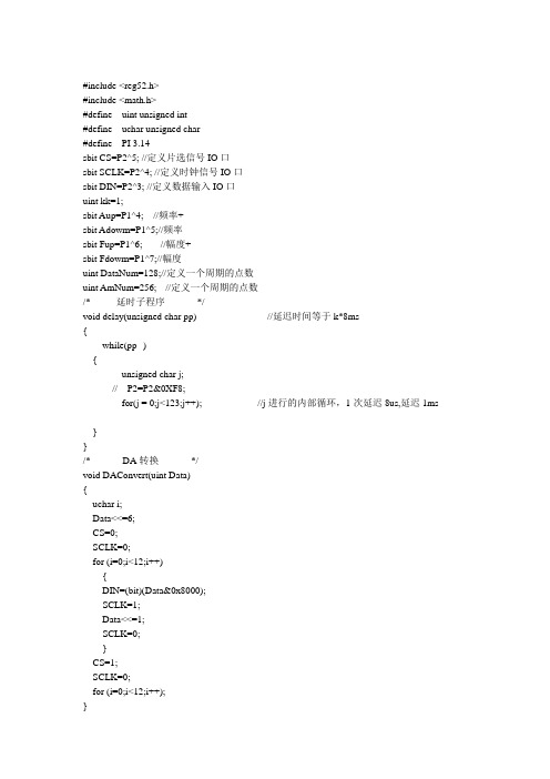
#include <reg52.h>#include <math.h>#define uint unsigned int#define uchar unsigned char#define PI 3.14sbit CS=P2^5; //定义片选信号IO口sbit SCLK=P2^4; //定义时钟信号IO口sbit DIN=P2^3; //定义数据输入IO口uint kk=1;sbit Aup=P1^4; //频率+sbit Adowm=P1^5;//频率-sbit Fup=P1^6; //幅度+sbit Fdowm=P1^7;//幅度-uint DataNum=128;//定义一个周期的点数uint AmNum=256; //定义一个周期的点数/*--------延时子程序----------*/void delay(unsigned char pp) //延迟时间等于k*8ms{while(pp--){unsigned char j;// P2=P2&0XF8;for(j = 0;j<123;j++); //j进行的内部循环,1次延迟8us,延迟1ms}}/*----------DA转换----------*/void DAConvert(uint Data){uchar i;Data<<=6;CS=0;SCLK=0;for (i=0;i<12;i++){DIN=(bit)(Data&0x8000);SCLK=1;Data<<=1;SCLK=0;}CS=1;SCLK=0;for (i=0;i<12;i++);}/*正弦波参数换算程序*/uint GetSinData(uchar x){uint SinData;SinData=((sin(2*PI*x/DataNum)+1)/2.0)*AmNum;return SinData;}/*----------主程序----------*/main(){uint i;while(1){for(i=0;i<DataNum;i++)DAConvert(GetSinData(i));//输出正弦波P1 = 0xFF; // 发全0行扫描码,列线输入if((P1&0xFF) != 0xFF) // 若有键按下{delay(1);// 延时去抖动if((P1&0xFF) != 0xFF)switch(AmNum){case 512: AmNum=256;break;case 32: AmNum=256; break;}switch(DataNum){case 256: DataNum=128;break;case 16: DataNum=128; break;}switch(P1){case 0x7f: AmNum=AmNum+32;break;//幅度+case 0xbf: AmNum=AmNum-32; break;//幅度-case 0xdf: DataNum=DataNum+16; break;//频率-case 0xef: DataNum=DataNum-16; break;//频率+}}}}。
TLC5615C, TLC5615I数据手册

1 2 3 48 7 6 5DIN SCLKCS DOUT V DDOUTREFINAGNDTLC5615C,TLC5615I SLAS142D–OCTOBER1996–REVISED AUGUST200310-BIT DIGITAL-TO-ANALOG CONVERTERSFEATURES•Settling Time to0.5LSB...12.5µs Typ•Monotonic Over Temperature•10-Bit CMOS Voltage Output DAC in an8-Terminal Package•Pin Compatible With the Maxim MAX515•5-V Single Supply OperationAPPLICATIONS•3-Wire Serial Interface•Battery-Powered Test Instruments•High-Impedance Reference Inputs•Digital Offset and Gain Adjustment•Voltage Output Range...2Times the Refer-ence Input Voltage•Battery Operated/Remote Industrial Controls •Internal Power-On Reset•Machine and Motion Control Devices•Low Power Consumption...1.75mW Max•Cellular Telephones•Update Rate of1.21MHzD,P,OR DGK PACKAGE(TOP VIEW)DESCRIPTIONThe TLC5615is a10-bit voltage output digital-to-analog converter(DAC)with a buffered reference input(high impedance).The DAC has an output voltage range that is two times the reference voltage,and the DAC is monotonic.The device is simple to use,running from a single supply of5V.A power-on-reset function is incorporated to ensure repeatable start-up conditions.Digital control of the TLC5615is over a three-wire serial bus that is CMOS compatible and easily interfaced to industry standard microprocessor and microcontroller devices.The device receives a16-bit data word to produce the analog output.The digital inputs feature Schmitt triggers for high noise immunity.Digital communication protocols include the SPI™,QSPI™,and Microwire™standards.The8-terminal small-outline D package allows digital control of analog functions in space-critical applications.The TLC5615C is characterized for operation from0°C to70°C.The TLC5615I is characterized for operation from-40°C to85°C.AVAILABLE OPTIONSPACKAGESMALL OUTLINE PLASTIC SMALL OUTLINE PLASTIC DIP T A(1)(D)(DGK)(P)0°C to70°C TLC5615CD TLC5615CDGK TLC5615CP40°C to85°C TLC5615ID TLC5615IDGK TLC5615IP(1)Available in tape and reel as the TLC5615CDR and the TLC5615IDRSPI,QSPI are trademarks of Motorola,Inc.Microwire is a trademark of National Semiconductor Corporation.Please be aware that an important notice concerning availability,standard warranty,and use in critical applications of Texas Instruments semiconductor products and disclaimers thereto appears at the end of this data sheet.查询TLC5615供应商捷多邦,专业PCB打样工厂,24小时加急出货REFIN AGNDCS SCLKDIN OUT(Voltage Output) DOUTTLC5615C,TLC5615ISLAS142D–OCTOBER1996–REVISED AUGUST2003FUNCTIONAL BLOCK DIAGRAMTerminal FunctionsTERMINALI/O DESCRIPTIONNAME NO.DIN1I Serial data inputSCLK2I Serial clock inputCS3I Chip select,active lowDOUT4O Serial data output for daisy chainingAGND5Analog groundREFIN6I Reference inputOUT7O DAC analog voltage outputV DD8Positive power supplyABSOLUTE MAXIMUM RATINGSover operating free-air temperature range(unless otherwise noted)(1)UNITSupply voltage(V DD to AGND)7VDigital input voltage range to AGND-0.3V to V DD+0.3VReference input voltage range to AGND-0.3V to V DD+0.3VOutput voltage at OUT from external source V DD+0.3VContinuous current at any terminal±20mAOperating free-air temperature range,T A TLC5615C0°C to70°CTLC5615I-40°C to85°CStorage temperature range,T stg-65°C to150°CLead temperature1,6mm(1/16inch)from case for10seconds260°C(1)Stresses beyond those listed under,,absolute maximum ratings”may cause permanent damage to the device.These are stressratings only,and functional operation of the device at these or any other conditions beyond those indicated under,,recommended operating conditions”is not implied.Exposure to absolute-maximum-rated conditions for extended periods may affect device reliability.TLC5615C,TLC5615I SLAS142D–OCTOBER1996–REVISED AUGUST2003RECOMMENDED OPERATING CONDITIONSMIN NOM MAX UNIT Supply voltage,V DD 4.55 5.5V High-level digital input voltage,V IH 2.4V Low-level digital input voltage,V IL0.8V Reference voltage,V ref to REFIN terminal2 2.048V DD-2V Load resistance,R L2kΩTLC5615C070°C Operating free-air temperature,T ATLC5615I4085°C ELECTRICAL CHARACTERISTICSover recommended operating free-air temperature range,V DD=5V±5%,V ref=2.048V(unless otherwise noted)STATIC DAC SPECIFICATIONSPARAMETER TEST CONDITIONS MIN TYP MAX UNIT Resolution10bits Integral nonlinearity,end point adjusted(INL)V ref=2.048V,See(1)±1LSB Differential nonlinearity(DNL)V ref=2.048V,See(2)±0.1±0.5LSBE ZS Zero-scale error(offset error at zero scale)V ref=2.048V,See(3)±3LSBZero-scale-error temperature coefficient V ref=2.048V,See(4)3ppm/°CE G Gain error V ref=2.048V,See(5)±3LSBGain-error temperature coefficient V ref=2.048V,See(6)1ppm/°CZero scale80PSRR Power-supply rejection ratio See(7)(8)dBGain80Analog full scale output R L=100kΩ2V ref(1023/1024)V (1)The relative accuracy or integral nonlinearity(INL),sometimes referred to as linearity error,is the maximum deviation of the outputfrom the line between zero and full scale excluding the effects of zero code and full-scale errors(see text).Tested from code3to code 1024.(2)The differential nonlinearity(DNL),sometimes referred to as differential error,is the difference between the measured and ideal1LSBamplitude change of any two adjacent codes.Monotonic means the output voltage changes in the same direction(or remains constant)as a change in the digital input code.Tested from code3to code1024.(3)Zero-scale error is the deviation from zero-voltage output when the digital input code is zero(see text).(4)Zero-scale-error temperature coefficient is given by:EZS TC=[E ZS(T max)-E ZS(T min)]/V ref×106/(T max-T min).(5)Gain error is the deviation from the ideal output(Vref -1LSB)with an output load of10kΩexcluding the effects of the zero-scale error.(6)Gain temperature coefficient is given by:EG TC=[E G(T max)-E G(T min)]/V ref×106/(T max-T min).(7)Zero-scale-error rejection ratio(EZS-RR)is measured by varying the VDD from4.5V to5.5V dc and measuring the proportion of thissignal imposed on the zero-code output voltage.(8)Gain-error rejection ratio(EG-RR)is measured by varying the VDD from4.5V to5.5V dc and measuring the proportion of this signalimposed on the full-scale output voltage after subtracting the zero-scale change.VOLTAGE OUTPUT(OUT)PARAMETER TEST CONDITIONS MIN TYP MAX UNIT V O Voltage output range R L=10kΩ0V DD-0.4V Output load regulation accuracy V O(OUT)=2V,R L=2kΩ0.5LSB I OSC Output short circuit current OUT to V DD or AGND20mA V OL(low)Output voltage,low-level I O(OUT)≤5mA0.25V V OH(high)Output voltage,high-level I O(OUT)≤-5mA 4.75V REFERENCE INPUT(REFIN)V I Input voltage0V DD-2V r i Input resistance10MΩTLC5615C,TLC5615ISLAS142D–OCTOBER 1996–REVISED AUGUST 2003VOLTAGE OUTPUT(OUT)(continued)PARAMETERTEST CONDITIONSMINTYP MAXUNIT C i Input capacitance5pFDIGITAL INPUTS (DIN,SCLK,CS)V IH High-level digital input voltage 2.4V V IL Low-level digital input voltage 0.8V I IH High-level digital input current V I =V DD ±1µA I IL Low-level digital input current V I =0±1µA C i Input capacitance 8pF DIGITAL OUTPUT (DOUT)V OH Output voltage,high-level I O =-2mA V DD -1V V OL Output voltage,low-level I O =2mA0.4V POWER SUPPLYV DD Supply voltage4.55 5.5V V DD =5.5V,No load,V ref =0150250µA All inputs =0V or V DD I DDPower supply currentV DD =5.5V,No load,V ref =2.048V230350µAAll inputs =0V or V DDANALOG OUTPUT DYNAMIC PERFORMANCEV ref =1V pp at 1kHz +2.048Vdc,Signal-to-noise +distortion,S/(N+D)code =1111111111,60dBSee (1)(1)The limiting frequency value at 1Vpp is determined by the output-amplifier slew rate.DIGITAL INPUT TIMING REQUIRMENTS (SEE FIGURE 1)PARAMETERMIN NOMMAXUNIT t su(DS)Setup time,DIN before SCLK high 45ns t h(DH)Hold time,DIN valid after SCLK high 0ns t su(CSS)Setup time,CS low to SCLK high 1ns t su(CS1)Setup time,CS high to SCLK high 50ns t h(CSH0)Hold time,SCLK low to CS low 1ns t h(CSH1)Hold time,SCLK low to CS high0ns t w(CS)Pulse duration,minimum chip select pulse width high 20ns t w(CL)Pulse duration,SCLK low 25ns t w(CH)Pulse duration,SCLK high25nsOUTPUT SWITCHING CHARACTERISTICSPARAMETERTEST CONDITIONSMIN NOM MAXUNIT t pd(DOUT)Propagation delay time,DOUTC L =50pF50nsOPERATING CHARACTERISTICSover recommended operating free-air temperature range,V DD =5V ±5%,V ref =2.048V (unless otherwise noted)PARAMETERTEST CONDITIONSMINTYPMAXUNITANALOG OUTPUT DYNAMIC PERFORMANCE C L =100pF,SROutput slew rateR L =10k Ω,0.30.5V/µsT A =25°CNOTES: A.The input clock, applied at the SCLK terminal, should be inhibited low when CS is high to minimize clock feedthrough.B.Data input from preceeding conversion cycle.C.Sixteenth SCLK falling edgeTLC5615C,TLC5615ISLAS142D–OCTOBER 1996–REVISED AUGUST 2003OPERATING CHARACTERISTICS (continued)over recommended operating free-air temperature range,V DD =5V ±5%,V ref =2.048V (unless otherwise noted)PARAMETERTEST CONDITIONSMINTYPMAXUNITANALOG OUTPUT DYNAMIC PERFORMANCE To 0.5LSB,C L =100pF,t sOutput settling time 12.5µs R L =10k Ω,See (1)Glitch energyDIN =All 0s to all 1s5nV •sREFERENCE INPUT (REFIN)Reference feedthrough REFIN =1V pp at 1kHz +2.048Vdc (see (2)-80dB Reference input REFIN =0.2V pp +2.048Vdc30kHzbandwidth (f-3dB)(1)Settling time is the time for the output signal to remain within ±0.5LSB of the final measured value for a digital input code change of 000hex to 3FF hex or 3FF hex to 000hex.(2)Reference feedthrough is measured at the DAC output with an input code =000hex and a V ref input =2.048Vdc +1V pp at 1kHz.PARAMETER MEASURMENT INFORMATIONFigure 1.Timing Diagram151050202530- O u t p u t S o u r c e C u r r e n t - m AI O V O - Output Pullup Voltage - V0.10.20.40.6- O u t p u t S i n k C u r r e n t - m A0.810.30.50.70.91.1 1.2I O V O - Output Pulldown Voltage - V80- S u p pl y C u r r e n t -20028024016012040-60-40-20020406080100120140Aµt - Temperature - °CI D D 11001 k10 k100 kG - R e l a t i v e G a i n - d B420-2-4-6-8-10-12-14f I - Input Frequency - HzTLC5615C,TLC5615ISLAS142D–OCTOBER 1996–REVISED AUGUST 2003TYPICAL CHARACTERISTICSOUTPUT SINK CURRENTOUTPUT SOURCE CURRENTvsvsOUTPUT PULLDOWN VOLTAGEFigure 2.Figure 3.V REFIN TO V (OUT)SUPPLY CURRENTRELATIVE GAINvsvsINPUT FREQUENCYFigure 4.Figure 5.40501 kS i g n a l -T o -N o i s e + D i s t o r t i o n - d B7030Frequency - Hz201006010 k 100 k 300 kD i f f e r e n t i a l N o n l i n e a r i t y – L S B–0.20.20.10–0.050.150.05–0.1–0.15Input Code2555117671023I n t e g r a l N o n l i n e a r i t y – L S B–0.6Input Code10–0.225551176710230.80.60.40.2–0.4–0.8–1TLC5615C,TLC5615ISLAS142D–OCTOBER 1996–REVISED AUGUST 2003TYPICAL CHARACTERISTICS (continued)SIGNAL-TO-NOISE +DISTORTIONvsINPUT FREQUENCY AT REFINFigure 6.Figure 7Differential Nonlinearity With Input CodeFigure 8Integral Nonlinearity With Input CodeOUTREFINCSTLC5615C,TLC5615ISLAS142D–OCTOBER 1996–REVISED AUGUST 2003APPLICATION INFORMATIONGENERAL FUNCTIONThe TLC5615uses a resistor string network buffered with an op amp in a fixed gain of 2to convert 10-bit digital data to analog voltage levels (see functional block diagram and Figure 9).The output of the TLC5615is the same polarity as the reference input (see Table 1).An internal circuit resets the DAC register to all zeros on power up.Figure 9.TLC5615Typical Operating CircuitTable 1.Binary Code Table (0V to 2V Output)Gain =2(1)A 10-bit data word with two bits below the LSB bit (sub-LSB)with 0values must be written since the DAC input latch is 12bits wide.BUFFER AMPLIFIERThe output buffer has a rail-to-rail output with short circuit protection and can drive a 2-k Ωload with a 100-pF load capacitance.Settling time is 12.5µs typical to within 0.5LSB of final value.f (SCLK)max +1t w ǒCH Ǔ)tw ǒCL Ǔt p(CS)+16 ǒtw ǒCH Ǔ)tw ǒCL ǓǓ)tw ǒCS Ǔ10 Data BitsxxMSB LSB2 Extra (Sub-LSB) Bitsx = don’t care10 Data BitsxxMSBLSB2 Extra (Sub-LSB) Bits4 Upper Dummy Bitsx = don’t careTLC5615C,TLC5615ISLAS142D–OCTOBER 1996–REVISED AUGUST 2003EXTERNAL REFERENCEThe reference voltage input is buffered,which makes the DAC input resistance not code dependent.Therefore,the REFIN input resistance is 10M Ωand the REFIN input capacitance is typically 5pF independent of input code.The reference voltage determines the DAC full-scale output.LOGIC INTERFACEThe logic inputs function with either TTL or CMOS logic levels.However,using rail-to-rail CMOS logic achieves the lowest power dissipation.The power requirement increases by approximately 2times when using TTL logic levels.SERIAL CLOCK AND UPDATE RATEFigure 1shows the TLC5615timing.The maximum serial clock rate is:or approximately 14MHz.The digital update rate is limited by the chip-select period,which is:and is equal to 820ns which is a 1.21MHz update rate.However,the DAC settling time to 10bits of 12.5µs limits the update rate to 80kHz for full-scale input step transitions.SERIAL INTERFACEWhen chip select (CS)is low,the input data is read into a 16-bit shift register with the input data clocked in most significant bit first.The rising edge of the SLCK input shifts the data into the input register.The rising edge of CS then transfers the data to the DAC register.When CS is high,input data cannot be clocked into the input register.All CS transitions should occur when the SCLK input is low.If the daisy chain (cascading)function (see daisy-chaining devices section)is not used,a 12-bit input data sequence with the MSB first can be used as shown in Figure 10:Figure 10.12-Bit Input Data Sequenceor 16bits of data can be transferred as shown in Figure 11with the 4upper dummy bits first.Figure 11.16-Bit Input Data SequenceNOTE A:The DOUT-SI connection is not required for writing tothe TLC5615 but may be used for verifying datatransfer if desired.NOTE A:The DOUT-MISO connection is not required for writing to theTLC5615 but may be used for verifying data transfer.CPOL = 0, CPHA = 0TLC5615C,TLC5615ISLAS142D–OCTOBER 1996–REVISED AUGUST 2003The data from DOUT requires 16falling edges of the input clock and,therefore,requires an extra clock width.When daisy chaining multiple TLC5615devices,the data requires 4upper dummy bits because the data transfer requires 16input-clock cycles plus one additional input-clock falling edge to clock out the data at the DOUT terminal (see Figure 1).The two extra (sub-LSB)bits are always required to provide hardware and software compatibility with 12-bit data converter transfers.The TLC5615three-wire interface is compatible with the SPI,QSPI †,and Microwire serial standards.The hardware connections are shown in Figure 12and Figure 13.The SPI and Microwire interfaces transfer data in 8-bit bytes,therefore,two write cycles are required to input data to the DAC.The QSPI interface,which has a variable input data length from 8to 16bits,can load the DAC input register in one write cycle.Figure 12.Microwire ConnectionFigure 13.SPI/QSPI ConnectionDAISY-CHAINING DEVICESDACs can be daisy-chained by connecting the DOUT terminal of one device to the DIN of the next device in the chain,providing that the setup time,t su(CSS),(CS low to SCLK high)is greater than the sum of the setup time,t su(DS),plus the propagation delay time,t pd(DOUT),for proper timing (see digital input timing requirements section).The data at DIN appears at DOUT,delayed by 16clock cycles plus one clock width.DOUT is a totem-poled output for low power.DOUT changes on the SCLK falling edge when CS is low.When CS is high,DOUT remains at the value of the last data bit and does not go into a high-impedance state.NegativeOffsetTLC5615C,TLC5615I SLAS142D–OCTOBER1996–REVISED AUGUST2003LINEARITY,OFSET,AND GAIN ERROR USING SINGLE ENDED SUPPLIESWhen an amplifier is operated from a single supply,the voltage offset can still be either positive or negative.With a positive offset,the output voltage changes on the first code change.With a negative offset the output voltage may not change with the first code depending on the magnitude of the offset voltage.The output amplifier attempts to drive the output to a negative voltage.However,because the most negative supply rail is ground,the output cannot drive below ground and clamps the output at0V.The output voltage then remains at zero until the input code value produces a sufficient positive output voltage to overcome the negative offset voltage,resulting in the transfer function shown in Figure14.Figure14.Effect of Negative Offset(Single Supply)This offset error,not the linearity error,produces this breakpoint.The transfer function would have followed the dotted line if the output buffer could drive below the ground rail.For a DAC,linearity is measured between zero-input code(all inputs0)and full-scale code(all inputs1)after offset and full scale are adjusted out or accounted for in some way.However,single supply operation does not allow for adjustment when the offset is negative due to the breakpoint in the transfer function.So the linearity is measured between full-scale code and the lowest code that produces a positive output voltage.For the TLC5615,the zero-scale(offset)error is plus or minus3LSB maximum.The code is calculated from the maximum specification for the negative offset.POWER-SUPPLY BYPASSING AND GROUND MANAGEMENTPrinted-circuit boards that use separate analog and digital ground planes offer the best system performance. Wire-wrap boards do not perform well and should not be used.The two ground planes should be connected together at the low-impedance power-supply source.The best ground connection may be achieved by connecting the DAC AGND terminal to the system analog ground plane making sure that analog ground currents are well managed and there are negligible voltage drops across the ground plane.A0.1-µF ceramic-capacitor bypass should be connected between V DD and AGND and mounted with short leads as close as possible to the e of ferrite beads may further isolate the system analog supply from the digital power supply.Figure15shows the ground plane layout and bypassing technique.TLC5615C,TLC5615ISLAS142D–OCTOBER 1996–REVISED AUGUST 2003Figure 15.Power-Supply BypassingSAVING POWERSetting the DAC register to all 0s minimizes power consumption by the reference resistor array and the output load when the system is not using the DAC.AC CONSIDERATIONSDigital FeedthroughEven with CS high,high-speed serial data at any of the digital input or output terminals may couple through the DAC package internal stray capacitance and appear at the DAC analog output as digital feedthrough.Digital feedthrough is tested by holding CS high and transmitting 010*******from DIN to DOUT.Analog FeedthroughHigher frequency analog input signals may couple to the output through internal stray capacitance.Analog feedthrough is tested by holding CS high,setting the DAC code to all 0s,sweeping the frequency applied to REFIN,and monitoring the DAC output.IMPORTANT NOTICETexas Instruments Incorporated and its subsidiaries (TI) reserve the right to make corrections, modifications, enhancements, improvements, and other changes to its products and services at any time and to discontinue any product or service without notice. Customers should obtain the latest relevant information before placing orders and should verify that such information is current and complete. All products are sold subject to TI’s terms and conditions of sale supplied at the time of order acknowledgment.TI warrants performance of its hardware products to the specifications applicable at the time of sale in accordance with TI’s standard warranty. Testing and other quality control techniques are used to the extent TI deems necessary to support this warranty. Except where mandated by government requirements, testing of all parameters of each product is not necessarily performed.TI assumes no liability for applications assistance or customer product design. Customers are responsible for their products and applications using TI components. To minimize the risks associated with customer products and applications, customers should provide adequate design and operating safeguards.TI does not warrant or represent that any license, either express or implied, is granted under any TI patent right, copyright, mask work right, or other TI intellectual property right relating to any combination, machine, or process in which TI products or services are used. Information published by TI regarding third-party products or services does not constitute a license from TI to use such products or services or a warranty or endorsement thereof. Use of such information may require a license from a third party under the patents or other intellectual property of the third party, or a license from TI under the patents or other intellectual property of TI.Reproduction of information in TI data books or data sheets is permissible only if reproduction is without alteration and is accompanied by all associated warranties, conditions, limitations, and notices. Reproduction of this information with alteration is an unfair and deceptive business practice. TI is not responsible or liable for such altered documentation.Resale of TI products or services with statements different from or beyond the parameters stated by TI for that product or service voids all express and any implied warranties for the associated TI product or service and is an unfair and deceptive business practice. TI is not responsible or liable for any such statements. Following are URLs where you can obtain information on other Texas Instruments products and application solutions:Products ApplicationsAmplifiers Audio /audioData Converters Automotive /automotiveDSP Broadband /broadbandInterface Digital Control /digitalcontrolLogic Military /militaryPower Mgmt Optical Networking /opticalnetwork Microcontrollers Security /securityTelephony /telephonyVideo & Imaging /videoWireless /wirelessMailing Address:Texas InstrumentsPost Office Box 655303 Dallas, Texas 75265Copyright 2003, Texas Instruments Incorporated。
用DA(TLC5615)芯片产生正弦波!

标签:基于AVR的正弦波发生器!【原创】用DA(TLC5615)芯片产生正弦波!附件里是一个好用的工具,《正弦波数据生成器》,精度可调!/************************************************CPU: MEGA64晶振:7.3728M功能:实现频率为25Hz的正弦波************************************************/#include<avr/io.h>#include<util/delay.h>#include<avr/eeprom.h>#include<avr/pgmspace.h>#include<avr/interrupt.h>#define uint8 unsigned char#define int8 signed char#define uint16 unsigned int#define int16 signed int#define uint32 unsigned long#define int32 signed long#define uchar unsigned char#define uint unsigned int/*----------------SPI端口定义-----------------*/#define MMC_SD_CS_DDR DDRB#define MMC_SD_CS_PORT PORTB#define MMC_SD_CS_BIT 0#define MMC_SD_SCK_DDR DDRB#define MMC_SD_SCK_PORT PORTB#define MMC_SD_SCK_BIT 1#define MMC_SD_MOSI_DDR DDRB#define MMC_SD_MOSI_PORT PORTB#define MMC_SD_MOSI_BIT 2#define MMC_SD_MISO_DDR DDRB#define MMC_SD_MISO_PORT PORTB#define MMC_SD_MISO_BIT 3#define MMC_SD_PORT_INI {\MMC_SD_CS_PORT |= 1<<MMC_SD_CS_BIT;\MMC_SD_SCK_PORT |= 1<<MMC_SD_SCK_BIT;\MMC_SD_MOSI_PORT |= 1<<MMC_SD_MOSI_BIT;\MMC_SD_MISO_PORT |= 1<<MMC_SD_MISO_BIT;\\MMC_SD_CS_DDR |= 1<<MMC_SD_CS_BIT;\MMC_SD_SCK_DDR |= 1<<MMC_SD_SCK_BIT;\MMC_SD_MOSI_DDR |= 1<<MMC_SD_MOSI_BIT;\MMC_SD_MISO_DDR &= ~(1<<MMC_SD_MISO_BIT);\}#define SPI_CS_Assert MMC_SD_CS_PORT &= ~(1<<MMC_SD_CS_BI T)#define SPI_CS_Deassert MMC_SD_CS_PORT |= 1<<MMC_SD_CS_BIT uint16 i="0";uint16 t="0";uint8 t1=0,t2=0;/*---------------------正弦波数据表---------------------------*/uint16 wave[1024]={0x1FF,0x202,0x205,0x208,0x20C,0x20F,0x212,0x215,0x218,0x21B,0x21E,0 x221,0x225,0x228,0x22B,0x22E,0x231,0x234,0x237,0x23A,0x23E,0x241,0x244,0x247,0x24A,0x24D,0x250,0 x253,0x256,0x25A,0x25D,0x260,0x263,0x266,0x269,0x26C,0x26F,0x272,0x275,0x278,0x27B,0x27E,0x281,0 x284,0x287,0x28A,0x28D,0x290,0x293,0x296,0x299,0x29C,0x29F,0x2A2,0x2A5,0x2A8,0x2AB,0x2AE,0x2B1, 0x2B4,0x2B7,0x2BA,0x2BD,0x2C0,0x2C3,0x2C6,0x2C9,0x2CB,0x2CE,0x2D1,0x2D4,0x2D7,0x2DA,0x2DD,0x2 DF,0x2E2,0x2E5,0x2E8,0x2EB,0x2ED,0x2F0,0x2F3,0x2F6,0x2F8,0x2FB,0x2FE,0x301,0x303,0x306,0x309,0x30B,0 x30E,0x311,0x313,0x316,0x319,0x31B,0x31E,0x320,0x323,0x326,0x328,0x32B,0x32D,0x330,0x332,0x335,0 x337,0x33A,0x33C,0x33F,0x341,0x343,0x346,0x348,0x34B,0x34D,0x34F,0x352,0x354,0x357,0x359,0x35B,0 x35D,0x360,0x362,0x364,0x366,0x369,0x36B,0x36D,0x36F,0x371,0x374,0x376,0x378,0x37A,0x37C,0x37E,0 x380,0x382,0x384,0x386,0x388,0x38A,0x38C,0x38E,0x390,0x392,0x394,0x396,0x398,0x39A,0x39C,0x39E, 0x39F,0x3A1,0x3A3,0x3A5,0x3A7,0x3A8,0x3AA,0x3AC,0x3AD,0x3AF,0x3B1,0x3B2,0x3B4,0x3B6,0x3B7,0x3B 9,0x3BA,0x3BC,0x3BE,0x3BF,0x3C1,0x3C2,0x3C4,0x3C5,0x3C6,0x3C8,0x3C9,0x3CB,0x3CC,0x3CD,0x3CF,0x3 D0,0x3D1,0x3D3,0x3D4,0x3D5,0x3D6,0x3D8,0x3D9,0x3DA,0x3DB,0x3DC,0x3DD,0x3DE,0x3E0,0x3E1,0x3E2,0x3 E3,0x3E4,0x3E5,0x3E6,0x3E7,0x3E8,0x3E8,0x3E9,0x3EA,0x3EB,0x3EC,0x3ED,0x3EE,0x3EE,0x3EF,0x3F0,0x3F 1,0x3F1,0x3F2,0x3F3,0x3F3,0x3F4,0x3F5,0x3F5,0x3F6,0x3F6,0x3F7,0x3F7,0x3F8,0x3F8,0x3F9,0x3F9,0x3FA,0 x3FA,0x3FB,0x3FB,0x3FB,0x3FC,0x3FC,0x3FC,0x3FD,0x3FD,0x3FD,0x3FD,0x3FE,0x3FE,0x3FE,0x3FE,0x3F E,0x3FE,0x3FE,0x3FE,0x3FE,0x3FE,0x3FE,0x3FE,0x3FE,0x3FE,0x3FE,0x3FE,0x3FE,0x3FE,0x3FE,0x3FE,0x3F E,0x3FD,0x3FD,0x3FD,0x3FD,0x3FC,0x3FC,0x3FC,0x3FB,0x3FB,0x3FB,0x3FA,0x3FA,0x3F9,0x3F9,0x3F8,0x3F8, 0x3F7,0x3F7,0x3F6,0x3F6,0x3F5,0x3F5,0x3F4,0x3F3,0x3F3,0x3F2,0x3F1,0x3F1,0x3F0,0x3EF,0x3EE,0x3EE, 0x3ED,0x3EC,0x3EB,0x3EA,0x3E9,0x3E8,0x3E8,0x3E7,0x3E6,0x3E5,0x3E4,0x3E3,0x3E2,0x3E1,0x3E0,0x3DE, 0x3DD,0x3DC,0x3DB,0x3DA,0x3D9,0x3D8,0x3D6,0x3D5,0x3D4,0x3D3,0x3D1,0x3D0,0x3CF,0x3CD,0x3CC,0x3 CB,0x3C9,0x3C8,0x3C6,0x3C5,0x3C4,0x3C2,0x3C1,0x3BF,0x3BE,0x3BC,0x3BA,0x3B9,0x3B7,0x3B6,0x3B4,0x3B 2,0x3B1,0x3AF,0x3AD,0x3AC,0x3AA,0x3A8,0x3A7,0x3A5,0x3A3,0x3A1,0x39F,0x39E,0x39C,0x39A,0x398,0x396, 0x394,0x392,0x390,0x38E,0x38C,0x38A,0x388,0x386,0x384,0x382,0x380,0x37E,0x37C,0x37A,0x378,0x376,0 x374,0x371,0x36F,0x36D,0x36B,0x369,0x366,0x364,0x362,0x360,0x35D,0x35B,0x359,0x357,0x354,0x352,0 x34F,0x34D,0x34B,0x348,0x346,0x343,0x341,0x33F,0x33C,0x33A,0x337,0x335,0x332,0x330,0x32D,0x32B,0 x328,0x326,0x323,0x320,0x31E,0x31B,0x319,0x316,0x313,0x311,0x30E,0x30B,0x309,0x306,0x303,0x301,0 x2FE,0x2FB,0x2F8,0x2F6,0x2F3,0x2F0,0x2ED,0x2EB,0x2E8,0x2E5,0x2E2,0x2DF,0x2DD,0x2DA,0x2D7,0x2D 4,0x2D1,0x2CE,0x2CB,0x2C9,0x2C6,0x2C3,0x2C0,0x2BD,0x2BA,0x2B7,0x2B4,0x2B1,0x2AE,0x2AB,0x2A8,0x2A 5,0x2A2,0x29F,0x29C,0x299,0x296,0x293,0x290,0x28D,0x28A,0x287,0x284,0x281,0x27E,0x27B,0x278,0x275,0 x272,0x26F,0x26C,0x269,0x266,0x263,0x260,0x25D,0x25A,0x256,0x253,0x250,0x24D,0x24A,0x247,0x244,0 x241,0x23E,0x23A,0x237,0x234,0x231,0x22E,0x22B,0x228,0x225,0x221,0x21E,0x21B,0x218,0x215,0x212,0 x20F,0x20C,0x208,0x205,0x202,0x1FF,0x1FC,0x1F9,0x1F6,0x1F2,0x1EF,0x1EC,0x1E9,0x1E6,0x1E3,0x1E0, 0x1DC,0x1D9,0x1D6,0x1D3,0x1D0,0x1CD,0x1CA,0x1C7,0x1C3,0x1C0,0x1BD,0x1BA,0x1B7,0x1B4,0x1B1,0x1A E,0x1AB,0x1A8,0x1A4,0x1A1,0x19E,0x19B,0x198,0x195,0x192,0x18F,0x18C,0x189,0x186,0x183,0x180,0x17D,0 x17A,0x177,0x174,0x171,0x16E,0x16B,0x168,0x165,0x162,0x15F,0x15C,0x159,0x156,0x153,0x150,0x14D,0 x14A,0x147,0x144,0x141,0x13E,0x13B,0x138,0x135,0x133,0x130,0x12D,0x12A,0x127,0x124,0x121,0x11F,0 x11C,0x119,0x116,0x113,0x111,0x10E,0x10B,0x108,0x106,0x103,0x100,0x0FD,0x0FB,0x0F8,0x0F5,0x0F3, 0x0F0,0x0ED,0x0EB,0x0E8,0x0E5,0x0E3,0x0E0,0x0DE,0x0DB,0x0D8,0x0D6,0x0D3,0x0D1,0x0CE,0x0CC,0x0 C9,0x0C7,0x0C4,0x0C2,0x0BF,0x0BD,0x0BB,0x0B8,0x0B6,0x0B3,0x0B1,0x0AF,0x0AC,0x0AA,0x0A7,0x0A5,0x0A 3,0x0A1,0x09E,0x09C,0x09A,0x098,0x095,0x093,0x091,0x08F,0x08D,0x08A,0x088,0x086,0x084,0x082,0x080,0 x07E,0x07C,0x07A,0x078,0x076,0x074,0x072,0x070,0x06E,0x06C,0x06A,0x068,0x066,0x064,0x062,0x060,0 x05F,0x05D,0x05B,0x059,0x057,0x056,0x054,0x052,0x051,0x04F,0x04D,0x04C,0x04A,0x048,0x047,0x045,0 x044,0x042,0x040,0x03F,0x03D,0x03C,0x03A,0x039,0x038,0x036,0x035,0x033,0x032,0x031,0x02F,0x02E,0 x02D,0x02B,0x02A,0x029,0x028,0x026,0x025,0x024,0x023,0x022,0x021,0x020,0x01E,0x01D,0x01C,0x01B,0 x01A,0x019,0x018,0x017,0x016,0x016,0x015,0x014,0x013,0x012,0x011,0x010,0x010,0x00F,0x00E,0x00D,0 x00D,0x00C,0x00B,0x00B,0x00A,0x009,0x009,0x008,0x008,0x007,0x007,0x006,0x006,0x005,0x005,0x004,0x 004,0x003,0x003,0x003,0x002,0x002,0x002,0x001,0x001,0x001,0x001,0x000,0x000,0x000,0x000,0x000,0x 000,0x000,0x000,0x000,0x000,0x000,0x000,0x000,0x000,0x000,0x000,0x000,0x000,0x000,0x000,0x000,0x 001,0x001,0x001,0x001,0x002,0x002,0x002,0x003,0x003,0x003,0x004,0x004,0x005,0x005,0x006,0x006,0x 007,0x007,0x008,0x008,0x009,0x009,0x00A,0x00B,0x00B,0x00C,0x00D,0x00D,0x00E,0x00F,0x010,0x010, 0x011,0x012,0x013,0x014,0x015,0x016,0x016,0x017,0x018,0x019,0x01A,0x01B,0x01C,0x01D,0x01E,0x020,0 x021,0x022,0x023,0x024,0x025,0x026,0x028,0x029,0x02A,0x02B,0x02D,0x02E,0x02F,0x031,0x032,0x033,0 x035,0x036,0x038,0x039,0x03A,0x03C,0x03D,0x03F,0x040,0x042,0x044,0x045,0x047,0x048,0x04A,0x04C,0 x04D,0x04F,0x051,0x052,0x054,0x056,0x057,0x059,0x05B,0x05D,0x05F,0x060,0x062,0x064,0x066,0x068,0 x06A,0x06C,0x06E,0x070,0x072,0x074,0x076,0x078,0x07A,0x07C,0x07E,0x080,0x082,0x084,0x086,0x088,0 x08A,0x08D,0x08F,0x091,0x093,0x095,0x098,0x09A,0x09C,0x09E,0x0A1,0x0A3,0x0A5,0x0A8,0x0AA,0x0AC, 0x0AF,0x0B1,0x0B3,0x0B6,0x0B8,0x0BB,0x0BD,0x0BF,0x0C2,0x0C4,0x0C7,0x0C9,0x0CC,0x0CE,0x0D1,0x0 D3,0x0D6,0x0D8,0x0DB,0x0DE,0x0E0,0x0E3,0x0E5,0x0E8,0x0EB,0x0ED,0x0F0,0x0F3,0x0F5,0x0F8,0x0FB,0x0FD, 0x100,0x103,0x106,0x108,0x10B,0x10E,0x111,0x113,0x116,0x119,0x11C,0x11F,0x121,0x124,0x127,0x12A,0 x12D,0x130,0x133,0x135,0x138,0x13B,0x13E,0x141,0x144,0x147,0x14A,0x14D,0x150,0x153,0x156,0x159,0 x15C,0x15F,0x162,0x165,0x168,0x16B,0x16E,0x171,0x174,0x177,0x17A,0x17D,0x180,0x183,0x186,0x189,0 x18C,0x18F,0x192,0x195,0x198,0x19B,0x19E,0x1A1,0x1A4,0x1A8,0x1AB,0x1AE,0x1B1,0x1B4,0x1B7,0x1BA, 0x1BD,0x1C0,0x1C4,0x1C7,0x1CA,0x1CD,0x1D0,0x1D3,0x1D6,0x1D9,0x1DD,0x1E0,0x1E3,0x1E6,0x1E9,0x1E C,0x1EF,0x1F2,0x1F6,0x1F9,0x1FC};/* spi low speed, below 400KHz */void SPI_Low(void){SPCR &= ~_BV(DORD);SPCR = _BV(SPE)|_BV(MSTR)|_BV(SPR0); SPSR &= ~_BV(SPI2X);}/* spi high speed, not exceed 25MHz */void SPI_High(void){SPCR &= ~_BV(DORD);//MSB在前SPCR = _BV(SPE)|_BV(MSTR);SPSR |= _BV(SPI2X);}/* read and write one byte , full duplex */ uint8 SPI_WriteByte(uint8 val){SPDR = val;while(!(SPSR & _BV(SPIF)));return SPDR;}void SPI_Init(void){MMC_SD_PORT_INI; /* Port Initialize */SPI_High();}void timer0_init(void){cli();TCCR0 = 0x00; //stopASSR = 0x00; //set async modeTCNT0 = 0xDC; //set countOCR0 = 0x24;TCCR0 = 0x02; //start timerTIMSK = 0x01; //timer interrupt sourcessei();}//T/C0中断例程SIGNAL(SIG_OVERFLOW0){TCNT0 = 0xE1;//40ust="wave"[i];t="t"<<2; //此处是重点,为何先左移2位,要搞懂mega64硬件spi模式,同时要搞懂tlc5615的12位数据传输模式。
TLC5615应用实例
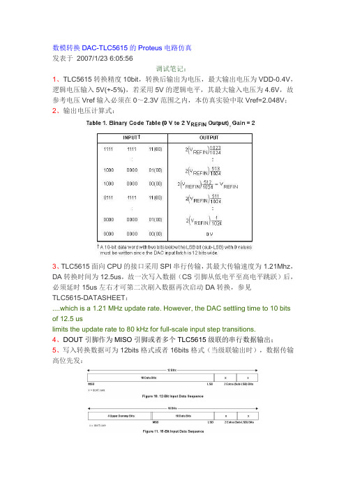
数模转换DAC-TLC5615的Proteus电路仿真发表于2007/1/23 6:05:56调试笔记:1、TLC5615转换精度10bit,转换后输出为电压,最大输出电压为VDD-0.4V,逻辑电压输入5V(+-5%),若采用5V的逻辑电平,其最大输入电压为4.6V,故参考电压Vref输入必须在0~2.3V范围之内,本仿真实验中取Vref=2.048V;2、输出电压计算式:3、TLC5615面向CPU的接口采用SPI串行传输,其最大传输速度为1.21Mhz,DA转换时间为12.5us,故一次写入数据(CS引脚从低电平至高电平跳跃)后,必须延时15us左右才可第二次刷入数据再次启动DA转换,参见TLC5615-DATASHEET:....which is a 1.21 MHz update rate. However, the DAC settling time to 10 bits of 12.5 uslimits the update rate to 80 kHz for full-scale input step transitions.4、DOUT引脚作为MISO引脚或者多个TLC5615级联的串行数据输出;5、写入转换数据可为12bits格式或者16bits格式(当级联输出时),数据传输高位先发:6、写时序与SPI兼容;7、模块子例程:/******************************************************************************/ /**/** 模块名:-------------------TLC5615.C---------------------------------/** -----------------数模转换子模块-----------------------------*//** 功能描述:/**/** 创建人:huangtiexiong 日期:2006-11-28 *//** 修改人:日期:2006-11-28 *//** 其他说明:/******************************************************************************/ #include "Includes.h" //文件包含/*************************************************模块级变量申明*************************************************/int8u bdata gBitMsb;sbit m7 = gBitMsb^7;int8u bdata gBitLsb;sbit l7 = gBitLsb^7;static void TLC5615_Write_12Bits();/*************************************************子函数定义*************************************************//********************************************************************************** 函数名: static void TLC5615_Write_12Bits()*** 功能描述: 一次向TLC中写入12bit数据;*** 全局变量: gBitMsb:待转换10bit高两位;gBitLsb:10bits的低8位;*** 输入: NO !*** 输出: NO !*** 创建人:huangtiexiong 日期:2006-11-28*** 修改人:日期:2006-11-28*** 函数说明: 内部函数;/******************************************************************************/ static void TLC5615_Write_12Bits(){int8u i;SCL = 0; //置零SCL,为写bit做准备;CS = 0;for(i=0;i<2;i++)//循2次,发送高两位;{if(m7) //高位先发;{SDA = 1; //将数据送出;SCL = 1; //提升时钟,写操作在时钟上升沿触发;SCL = 0; //结束该位传送,为下次写作准备;}else{SDA = 0;SCL = 1;SCL = 0;}gBitMsb <<= 1;}for(i=0;i<8;i++)//循环八次,发送低八位;{if(l7){SDA = 1; //将数据送出;SCL = 1; //提升时钟,写操作在时钟上升沿触发;SCL = 0; //结束该位传送,为下次写作准备;}else{SDA = 0;SCL = 1;SCL = 0;}gBitLsb <<= 1;}for(i=0;i<2;i++)//循环2次,发送两个虚拟位;{SDA = 0;SCL = 1;SCL = 0;}CS = 1;SCL = 0;}/********************************************************************************** 函数名: extern void TLC5615_Start(int16u dacDat)*** 功能描述: 启动DAC转换;*** 全局变量: gBitMsb:待转换10bit高两位;gBitLsb:10bits的低8位;*** 输入: dacDat:int16u;*** 输出: NO !*** 创建人:huangtiexiong 日期:2006-11-28*** 修改人:日期:2006-11-28*** 函数说明: 外部函数;/******************************************************************************/ extern void TLC5615_Start(int16u dacDat){dacDat %= 1024;gBitMsb = dacDat/256;gBitLsb = dacDat%256;gBitMsb <<= 6;TLC5615_Write_12Bits();}/******************************************************************************* **** End Of File*******************************************************************************/ 8、Proteus仿真抓图:。
TLC5615中文数据手册

二~二
注释, A、为了使时钟馈通为最小,当 CS为高电平时加在SCLK端的输入时钟应当呈现低电平. B 、数据输入来自先前转换周期. C、第 16个 SCLK下降沿 图 1 时序图
= = 98-4-22 :: 10:08 P&S武汉力源电子股份有限公司
10-6
吨 , 晶
AU 典
型
特
性 刽
曲
线
FH i 黠ii斗 俑
IIIN 1YP MAX UNIT 4.5 5 5.5 v
1 回 250 恤
230 捕。 M
2.3.7 模拟输出动态性能
R民RAMETER
国gn皿-..,..,01回+ dlstorUon, S/(N+D)
TEST 自由刷 DπIONB
W窗户 1 Vocat 1 kHz + 2.048 Vdc,
由蛐e= 咽啊'恻唱, S咽 No阳 8
帽
g"
申 吉
但
%
1/
E a
/
量 崎
' e e 9
J
"•• v / v
4
/
2
¢ MMMMMMM"'Mtz
v VO-OUtPUt PuIdown V.蝴匈..
图2 输出吸收电流与输出下拉电压的关系 280
;8339 刽←回E回Vg-gsrv蝴V
...
v ν, 伊'
vv
唱
v
:ær咱
1/
/ 一
-. U '-1 <<C.2 C 3.1且IU 3.2 3 胁。嘟ut Pl巅lPlMI幅画..V
电源电压 (Voo至AGND)
- 1、下载文档前请自行甄别文档内容的完整性,平台不提供额外的编辑、内容补充、找答案等附加服务。
- 2、"仅部分预览"的文档,不可在线预览部分如存在完整性等问题,可反馈申请退款(可完整预览的文档不适用该条件!)。
- 3、如文档侵犯您的权益,请联系客服反馈,我们会尽快为您处理(人工客服工作时间:9:00-18:30)。
调试笔记:
1、TLC5615转换精度10bit,转换后输出为电压,最大输出电压为VDD-0.4V,逻辑电压输入5V(+-5%),若采用5V的逻辑电平,其最大输入电压为4.6V,故参考电压Vref输入必须在0~2.3V范围之内,本仿真实验中取Vref=2.048V;
2、输出电压计算式:
3、TLC5615面向CPU的接口采用SPI串行传输,其最大传输速度为1.21Mhz,DA转换时间为12.5us,故一次写入数据(CS引脚从低电平至高电平跳跃)后,必须延时15us左右才可第二次刷入数据再次启动DA转换,参见
TLC5615-DATASHEET:
....which is a 1.21 MHz update rate. However, the DAC settling time to 10 bits of 12.5 us
limits the update rate to 80 kHz for full-scale input step transitions.
4、DOUT引脚作为MISO引脚或者多个TLC5615级联的串行数据输出;
5、写入转换数据可为12bits格式或者16bits格式(当级联输出时),数据传输高位先发:
6、写时序与SPI兼容;。