常用电源芯片手册
dcdc芯片手册

DC-DC芯片手册1. 引言DC-DC芯片作为电源管理系统中的核心组件之一,扮演着将直流电压转换为其他直流电压的重要角色。
本文将深入探讨DC-DC芯片的技术特点、应用场景以及手册的编写与使用。
1.1 DC-DC芯片的基本概念介绍DC-DC芯片的基本概念,阐述其在电源管理中的作用,以及在不同电子设备中的广泛应用。
1.2 DC-DC芯片手册的重要性强调DC-DC芯片手册在设计、调试和维护电源系统中的重要性,以及为用户提供准确信息的必要性。
2. 技术特点与规格详细介绍DC-DC芯片的技术特点和规格,使读者对该芯片有一个全面的了解。
2.1 输入与输出电压范围阐述DC-DC芯片所支持的输入和输出电压范围,以及在不同工作条件下的稳定性和性能。
2.2 效率与功率密度探讨DC-DC芯片的能效表现,包括效率的计算方法和功率密度的重要性。
2.3 转换拓扑与控制方式介绍不同DC-DC芯片的转换拓扑结构和控制方式,以及它们在实际应用中的优劣和适用场景。
3. 电路连接与布局建议提供DC-DC芯片在电路中的连接方式和布局建议,以确保最佳性能和稳定性。
3.1 输入输出电容的选择详细讨论在设计中如何选择适当的输入和输出电容,以保障电源系统的稳定性。
3.2 输入输出滤波电感的应用阐述滤波电感在DC-DC芯片电路中的作用,以及如何选择和应用合适的滤波电感。
3.3 PCB布局与散热设计探讨PCB布局对DC-DC芯片性能的影响,以及良好的散热设计对延长芯片寿命的重要性。
4. 保护特性与故障诊断详细介绍DC-DC芯片的保护特性,以及在故障发生时的诊断方法。
4.1 过流与过压保护讨论DC-DC芯片在过流和过压情况下的保护机制,确保电源系统的安全稳定运行。
4.2 温度保护与限流功能阐述芯片的温度保护机制和限流功能,以应对在高温或过载情况下可能出现的问题。
5. DC-DC芯片手册的编写与更新探讨编写DC-DC芯片手册的步骤和要点,以及在新版本发布时如何进行更新。
ap6335芯片手册
ap6335芯片手册**一、AP6335芯片简介**AP6335是一款由某公司生产的芯片,主要用于各种电子设备的电源管理。
该芯片具有高性能、低功耗的特点,能满足不同场合的需求。
在这篇文章中,我们将详细介绍AP6335芯片的主要特性、应用领域以及相关规格参数。
**二、AP6335芯片主要特性**1.高性能:AP6335具有较高的开关频率,可在较短时间内完成电源转换,提高设备工作效率。
2.低功耗:该芯片在待机状态下具有较低的功耗,有助于降低设备能耗,提高续航能力。
3.出色的电磁干扰性能:AP6335采用了先进的电磁干扰抑制技术,有效降低了电磁干扰,提高了设备稳定性。
4.宽电压范围:该芯片适用于广泛的电压输入范围,适应性强。
5.灵活的输出配置:AP6335支持多种输出配置,可根据不同设备需求进行调整。
**三、AP6335芯片应用领域**1.智能手机、平板电脑等移动设备电源管理。
2.笔记本电脑、服务器等电子设备的电源供应。
3.通信设备、网络设备等高性能电子设备的电源管理。
4.工业控制、自动化设备等领域的高效电源管理。
**四、AP6335芯片规格参数**1.工作电压:输入电压范围宽,适用于不同场合。
2.输出电压:根据应用需求,可调整输出电压。
3.电流容量:具有较大的电流容量,满足高负载需求。
4.开关频率:较高开关频率,提高电源转换效率。
5.封装形式:多种封装形式,便于设计布局。
**五、总结**AP6335芯片作为一款高性能、低功耗的电源管理芯片,广泛应用于各类电子设备中。
其优秀的特性和丰富的应用领域使其成为电源管理领域的理想选择。
在实际应用中,根据设备需求选择合适的AP6335芯片规格参数,可实现高效、稳定的电源管理。
ldo稳压芯片手册

ldo稳压芯片手册LDO(Low Dropout Regulator)稳压芯片是一种常见的电源管理芯片,用于提供稳定的直流电压。
以下是对LDO稳压芯片的手册介绍:一、概述LDO稳压芯片是一种低压差线性稳压器,能够在输入电压和输出电压之间产生较低的电压差,同时提供稳定的输出电压。
与开关电源相比,LDO稳压芯片具有较低的噪声和较小的纹波,因此广泛应用于各种电子设备中,如手机、平板电脑、充电器等。
二、工作原理LDO稳压芯片的工作原理是通过调整内部晶体管的导通电阻来控制输出电压。
当输入电压发生变化时,内部晶体管的导通电阻也会相应调整,从而保持输出电压的稳定。
同时,LDO稳压芯片还具有过流保护、过温保护等保护功能,以确保芯片的安全运行。
三、性能参数1.输入电压范围:LDO稳压芯片的输入电压范围通常在2-10V之间,具体范围取决于不同型号的芯片。
2.输出电压:输出电压是LDO稳压芯片的主要参数之一,可以根据不同的应用需求进行选择,常见的输出电压有1.8V、3.3V、5V等。
3.负载电流:负载电流是指LDO稳压芯片能够提供的最大输出电流,通常在几十毫安到几安培之间。
4.电压差:电压差是指LDO稳压芯片的输入电压与输出电压之间的差值,通常在0.2-1V之间。
5.噪声和纹波:LDO稳压芯片的噪声和纹波较低,可以提供较为稳定的输出电压。
四、应用场景1.手机、平板电脑等移动设备:在这些设备中,LDO稳压芯片被用于提供稳定的电源电压,以确保设备的正常运行。
2.充电器:充电器中的LDO稳压芯片用于将输入的交流电压转换为稳定的直流电压,以供电池充电使用。
3.音频设备:在音频设备中,LDO稳压芯片被用于提供稳定的电源电压,以确保音频信号的稳定传输。
4.工业控制:在工业控制系统中,LDO稳压芯片被用于提供稳定的电源电压,以确保控制系统的正常运行。
总之,LDO稳压芯片是一种重要的电源管理芯片,具有广泛的应用前景。
在实际应用中,需要根据具体需求选择合适的型号和参数,以确保系统的稳定性和可靠性。
BZT52系列单极性电源芯片数据手册说明书

BZT52 seriesSingle Zener diodes in a SOD123 packageRev. 1 — 16 March 2017Product data sheet1Product profile1.1General descriptionGeneral-purpose Zener diodes in a SOD123 small Surface-Mounted Device (SMD)plastic package.1.2Features and benefits•Total power dissipation: ≤ 590 mW•Wide working voltage range: nominal 2.4 V to 75 V (E24 range)•Small plastic package suitable for surface-mounted design •Low differential resistance •AEC-Q101 qualified1.3Applications•General regulation functions1.4Quick reference data[1]Pulse test: t p ≤ 300 μs; δ ≤ 0.02.[2]Device mounted on an FR4 Printed-Circuit Board (PCB), single-sided copper, tin-plated and standard footprint.[3]Device mounted on an FR4 PCB, single-sided copper, tin-plated, mounting pad for cathode 1 cm 2.Single Zener diodes in a SOD123 package 2Pinning information[1]The marking bar indicates the cathode.3Ordering information[1]The series consists of 37 types with nominal working voltages from 2.4 V to 75 V.4MarkingSingle Zener diodes in a SOD123 package 5Limiting valuesTable 5. Limiting valuesIn accordance with the Absolute Maximum Rating System (IEC 60134).[1]t p = 100 μs; square wave; T j = 25 °C prior to surge.[2]Device mounted on an FR4 PCB, single-sided copper, tin-plated and standard footprint.[3]Device mounted on an FR4 PCB, single-sided copper, tin-plated, mounting pad for cathode 1 cm2.6Thermal characteristics[1]Device mounted on an FR4 Printed-Circuit Board (PCB),single-sided copper, tin-plated and standard footprint.[2]Device mounted on an FR4 PCB, single-sided copper, tin-plated, mounting pad for cathode 1 cm2.[3]Soldering point of cathode tab.7CharacteristicsTable 7. CharacteristicsT = 25 °C unless otherwise specified.[1]Pulse test: t p ≤ 300 μs; δ ≤ 0.02.Single Zener diodes in a SOD123 package Table 8. Characteristics per type; BZT52-C2V4 to BZT52-C24= 25 °C unless otherwise specified.T[1] f = 1 MHz; V R = 0 V.[2]t p = 100 μs; T amb = 25 °C.Single Zener diodes in a SOD123 packageTable 9. Characteristics per type; BZT52-C27 to BZT52-C51T= 25 °C unless otherwise specified.[1] f = 1 MHz; V R = 0 V.[2]t p = 100 μs; T amb = 25 °C.Table 10. Characteristics per type; BZT52-C56 to BZT52-C75T = 25 °C unless otherwise specified.[1] f = 1 MHz; V R = 0 V.[2]t p = 100 μs; T amb = 25 °C.Single Zener diodes in a SOD123 package8Test information8.1Quality informationThis product has been qualified in accordance with the Automotive Electronics Council(AEC) standard Q101 - Stress test qualification for discrete semiconductors, and issuitable for use in automotive applications.Single Zener diodes in a SOD123 package9Package outline10Packing informationTable 11. Packing methodsThe indicated -xxx are the last three digits of the 12NC ordering code.Single Zener diodes in a SOD123 package 11SolderingSingle Zener diodes in a SOD123 package 12Revision historySingle Zener diodes in a SOD123 package 13Legal information13.1 Data sheet status[1]Please consult the most recently issued document before initiating or completing a design.[2]The term 'short data sheet' is explained in section "Definitions".[3]The product status of device(s) described in this document may have changed since this document was published and may differ in case of multipledevices. The latest product status information is available on the Internet at URL .13.2 DefinitionsDraft — The document is a draft version only. The content is still under internal review and subject to formal approval, which may result in modifications or additions. Nexperia does not give any representations or warranties as to the accuracy or completeness of information included herein and shall have no liability for the consequences of use of such information.Short data sheet — A short data sheet is an extract from a full data sheet with the same product type number(s) and title. A short data sheet is intended for quick reference only and should not be relied upon to contain detailed and full information. For detailed and full information see the relevant full data sheet, which is available on request via the local Nexperia sales office. In case of any inconsistency or conflict with the short data sheet, the full data sheet shall prevail.Product specification — The information and data provided in a Product data sheet shall define the specification of the product as agreed between Nexperia and its customer, unless Nexperia and customer have explicitly agreed otherwise in writing. In no event however, shall an agreement be valid in which the Nexperia product is deemed to offer functions and qualities beyond those described in the Product data sheet.13.3 DisclaimersLimited warranty and liability — Information in this document is believed to be accurate and reliable. However, Nexperia does not give any representations or warranties, expressed or implied, as to the accuracyor completeness of such information and shall have no liability for the consequences of use of such information. Nexperia takes no responsibility for the content in this document if provided by an information source outside of Nexperia. In no event shall Nexperia be liable for any indirect, incidental, punitive, special or consequential damages (including - without limitation -lost profits, lost savings, business interruption, costs related to the removal or replacement of any products or rework charges) whether or not such damages are based on tort (including negligence), warranty, breach of contract or any other legal theory. Notwithstanding any damages that customer might incur for any reason whatsoever, Nexperia's aggregate and cumulative liability towards customer for the products described herein shall be limited in accordance with the Terms and conditions of commercial sale of Nexperia.Right to make changes — Nexperia reserves the right to make changesto information published in this document, including without limitation specifications and product descriptions, at any time and without notice. This document supersedes and replaces all information supplied prior to the publication hereof.Suitability for use — Nexperia products are not designed, authorized or warranted to be suitable for use in life support, life-critical or safety-critical systems or equipment, nor in applications where failure or malfunctionof an Nexperia product can reasonably be expected to result in personal injury, death or severe property or environmental damage. Nexperia and its suppliers accept no liability for inclusion and/or use of Nexperia products in such equipment or applications and therefore such inclusion and/or use is at the customer’s own risk.Applications — Applications that are described herein for any of these products are for illustrative purposes only. Nexperia makes no representation or warranty that such applications will be suitable for the specified use without further testing or modification. Customers are responsible for the design and operation of their applications and products using Nexperia products, and Nexperia accepts no liability for any assistance with applications or customer product design. It is customer’s sole responsibility to determine whether the Nexperia product is suitable and fit for the customer’s applications and products planned, as well as for the planned application and use of customer’s third party customer(s). Customers should provide appropriate design and operating safeguards to minimize the risks associated with their applications and products. Nexperia does not accept any liability related to any default, damage, costs or problem which is based on any weakness or default in the customer’s applications or products, or the application or use by customer’s third party customer(s). Customer is responsible for doing all necessary testing for the customer’s applications and products using Nexperia products in order to avoid a default of the applications and the products or of the application or use by customer’s third party customer(s). Nexperia does not accept any liability in this respect.Limiting values — Stress above one or more limiting values (as defined in the Absolute Maximum Ratings System of IEC 60134) will cause permanent damage to the device. Limiting values are stress ratings only and (proper) operation of the device at these or any other conditions above thosegiven in the Recommended operating conditions section (if present) or the Characteristics sections of this document is not warranted. Constant or repeated exposure to limiting values will permanently and irreversibly affect the quality and reliability of the device.Terms and conditions of commercial sale — Nexperia products aresold subject to the general terms and conditions of commercial sale, as published at /profile/terms, unless otherwise agreed in a valid written individual agreement. In case an individual agreement is concluded only the terms and conditions of the respective agreement shall apply. Nexperia hereby expressly objects to applying the customer’s general terms and conditions with regard to the purchase of Nexperia products by customer.No offer to sell or license — Nothing in this document may be interpreted or construed as an offer to sell products that is open for acceptance orthe grant, conveyance or implication of any license under any copyrights, patents or other industrial or intellectual property rights.Export control — This document as well as the item(s) described herein may be subject to export control regulations. Export might require a prior authorization from competent authorities.Single Zener diodes in a SOD123 packageNon-automotive qualified products — Unless this data sheet expressly states that this specific Nexperia product is automotive qualified, the product is not suitable for automotive use. It is neither qualified nor tested in accordance with automotive testing or application requirements. Nexperia accepts no liability for inclusion and/or use of non-automotive qualified products in automotive equipment or applications. In the event that customer uses the product for design-in and use in automotive applications to automotive specifications and standards, customer (a) shall use the product without Nexperia's warranty of the product for such automotive applications, use and specifications, and (b) whenever customer uses the product for automotive applications beyond Nexperia's specifications such use shall be solely at customer’s own risk, and (c) customer fully indemnifies Nexperia for any liability, damages or failed product claims resulting from customer design and use of the product for automotive applications beyond Nexperia's standard warranty and Nexperia's product specifications.Translations — A non-English (translated) version of a document is for reference only. The English version shall prevail in case of any discrepancy between the translated and English versions.13.4 TrademarksNotice: All referenced brands, product names, service names and trademarks are the property of their respective owners.Single Zener diodes in a SOD123 package TablesTab. 1.Quick reference data (1)Tab. 2.Pinning (2)Tab. 3.Ordering information (2)Tab. 4.Marking codes (2)Tab. 5.Limiting values (3)Tab. 6.Thermal characteristics (3)Tab. 7.Characteristics ...................................................3Tab. 8.Characteristics per type; BZT52-C2V4 toBZT52-C24 (4)Tab. 9.Characteristics per type; BZT52-C27 toBZT52-C51 (5)Tab. 10.Characteristics per type; BZT52-C56 toBZT52-C75 (5)Tab. 11.Packing methods (7)Tab. 12.Revision history (9)FiguresFig. 1.Non-repetitive peak reverse powerdissipation as a function of pulse duration;maximum values (6)Fig. 2.Forward current as a function of forwardvoltage; typical values .......................................6Fig. 3.Temperature coefficient as a function ofworking current; typical values (6)Fig. 4.Temperature coefficient as a function ofworking current; typical values (6)Fig. 5.Package outline SOD123 (7)Fig. 6.Reflow soldering footprint SOD123 (8)Single Zener diodes in a SOD123 packagePlease be aware that important notices concerning this document and the product(s)described herein, have been included in section 'Legal information'.Contents1Product profile ....................................................11.1General description ............................................11.2Features and benefits ........................................11.3Applications ........................................................11.4Quick reference data .........................................12Pinning information ............................................23Ordering information ..........................................24Marking .................................................................25Limiting values ....................................................36Thermal characteristics ......................................37Characteristics ....................................................38Test information ..................................................68.1Quality information .............................................69Package outline ...................................................710Packing information ............................................711Soldering ..............................................................812Revision history .. (913)Legal information (10)Mouser ElectronicsAuthorized DistributorClick to View Pricing, Inventory, Delivery & Lifecycle Information:N experia:BZT52-C10J BZT52-C12X BZT52-C15X BZT52-C16X BZT52-C18X BZT52-C5V6J BZT52-C6V2X BZT52-C7V5X BZT52-C8V2J BZT52-C33J BZT52-C39J BZT52-C3V3X BZT52-C3V9X BZT52-C4V7J BZT52-C5V1J BZT52-C11J BZT52-C22X BZT52-C24J BZT52-C7V5J BZT52-C2V7J BZT52-C30J BZT52-C39X BZT52-C36J BZT52-C6V8X BZT52-C15J BZT52-C51X BZT52-C10X BZT52-C56X BZT52-C13J BZT52-C51J BZT52-C20J BZT52-C2V7X BZT52-C27J BZT52-C4V3X BZT52-C56J BZT52-C62J BZT52-C33X BZT52-C12J BZT52-C3V3J BZT52-C3V9J BZT52-C68J BZT52-C75J BZT52-C43J BZT52-C3V6J BZT52-C24X BZT52-C3V6X BZT52-C62X BZT52-C9V1X BZT52-C47J BZT52-C30X BZT52-C11X BZT52-C68X BZT52-C36X BZT52-C47X BZT52-C27X BZT52-C2V4J BZT52-C5V1X BZT52-C13X BZT52-C22J BZT52-C9V1J BZT52-C4V3J BZT52-C6V8J BZT52-C18JBZT52-C16J BZT52-C3V0X BZT52-C75X BZT52-C43X BZT52-C2V4X BZT52-C4V7X BZT52-C20X BZT52-C8V2X BZT52-C3V0J BZT52-C6V2J BZT52-C5V6X。
NCP1117 电源芯片数据手册
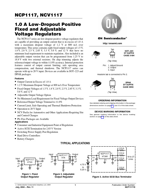
NCP1117, NCV11171.0 A Low−Dropout Positive Fixed and Adjustable Voltage RegulatorsThe NCP1117 series are low dropout positive voltage regulators that are capable of providing an output current that is in excess of 1.0 A with a maximum dropout voltage of 1.2 V at 800 mA over temperature. This series contains eight fixed output voltages of 1.5 V, 1.8 V, 2.0 V, 2.5 V, 2.85 V, 3.3 V, 5.0 V, and 12 V that have no minimum load requirement to maintain regulation. Also included is an adjustable output version that can be programmed from 1.25 V to 18.8 V with two external resistors. On chip trimming adjusts the reference/output voltage to within ±1.0% accuracy. Internal protection features consist of output current limiting, safe operating area compensation, and thermal shutdown. The NCP1117 series can operate with up to 20 V input. Devices are available in SOT−223 and DPAK packages.Features•Output Current in Excess of 1.0 A•1.2 V Maximum Dropout V oltage at 800 mA Over Temperature •Fixed Output V oltages of 1.5 V, 1.8 V, 2.0 V, 2.5 V, 2.85 V, 3.3 V, 5.0 V, and 12 V•Adjustable Output V oltage Option•No Minimum Load Requirement for Fixed V oltage Output Devices •Reference/Output V oltage Trimmed to ±1.0%•Current Limit, Safe Operating and Thermal Shutdown Protection •Operation to 20 V Input•NCV Prefix for Automotive and Other Applications Requiring Site and Control Changes•Pb−Free Packages are AvailableApplications•Consumer and Industrial Equipment Point of Regulation •Active SCSI Termination for 2.85 V Version•Switching Power Supply Post Regulation•Hard Drive Controllers•Battery ChargersFigure 1. Fixed Output RegulatorFigure 2. AdjustableOutput RegulatortoFigure 3. Active SCSI Bus Terminator TYPICAL APPLICATIONSSee detailed ordering and shipping information in the packagedimensions section on pages 11 and 12 of this data sheet.ORDERING INFORMATIONSee general marking information in the device markingsection on page 13 of this data sheet.DEVICE MARKING INFORMATIONMaximum ratings are those values beyond which device damage can occur. Maximum ratings applied to the device are individual stress limit values (not normal operating conditions) and are not valid simultaneously. If these limits are exceeded, device functional operation is not implied, damage may occur and reliability may be affected.1.This device series contains ESD protection and exceeds the following tests:Human Body Model 2000 V per MIL−STD−883, Method 3015.Machine Model Method 200 V.2.Internal thermal shutdown protection limits the die temperature to approximately 175°C. Proper heatsinking is required to prevent activation.The maximum package power dissipation is:P D+T J(max)*T AR q JA3.The regulator output current must not exceed 1.0 A with V in greater than 12 V.4.Low duty cycle pulse techniques are used during testing to maintain the junction temperature as close to ambient as possible.5.The regulator output current must not exceed 1.0 A with V in greater than 12 V.6.NCP1117: T low = 0°C ,T high = 125°CNCV1117: T low = −40°C,T high = 125°C7.NCP1117: T low = 0°C ,T high = 125°CNCV1117: T low = −40°C,T high = 125°CT A , AMBIENT TEMPERATURE (°C)I a d j , A D J U S T P I N C U R R E N T (m A )020406080100Figure 8. Adjust Pin Currentvs. Temperature Figure 9. Quiescent Current Changevs. Temperature2.0I o u t , O U T P U T C U R R E N T (A )V o u t , O U T P U T V O L T A G E C H A N G E (%)−50−250255075100125150T A , AMBIENT TEMPERATURE (°C)−50−25255075100125150t, TIME (m s)−2007.56.54080120160O U T P U T V O L T A G E D E V I A T I O N (m V )I N P U T V O L T A G E (V )20020020406080100101001.0 k10 k100 k204060801002004006008001000I out , OUTPUT CURRENT (mA)R R , R I P P L E R E J E C T I O N (d B )f ripple , RIPPLE FREQUENCY (Hz)R R , R I P P L E R E J E C T I O N(d B )Figure 10. NCP1117XTA Ripple Rejectionvs. Output CurrentFigure 11. NCP1117XTA Ripple Rejectionvs. FrequencyFigure 12. NCP1117XT285Line Transient ResponseFigure 13. NCP1117XT285Load Transient ResponseFigure 14. NCP1117XT50Line Transient Response Figure 15. NCP1117XT50Load Transient ResponseC in = 10 m F C out = 10 m F V in = 6.5 VPreload = 0.1 A T A = 25°Ct, TIME (m s)00.500.1−0.14080120160L O A D C U R R E N T C H A N G E (A )O U T P U T V O L T A G E D E V I A T I O N (V )200C in = 10 m F C out = 10 m F V in = 4.5 VPreload = 0.1 A T A = 25°Ct, TIME (m s)00.500.1−0.14080120160L O A D C U R R E N T C H A N G E (A )O U T P U T V O L T A G E D E V I A T I O N (V )200t, TIME (m s)−2005.254.254080120160O U T P U T V O L T A G E D E V I A T I O N (m V )I N P U T V O L T A G E (V )200C in = 1.0 m F C out = 10 m F I out = 0.1 A T A = 25°C20C in = 1.0 m F C out = 10 m F I out = 0.1 A T A = 25°CFigure 16. NCP1117XT12 LineTransient ResponseFigure 17. NCP1117XT12 LoadTransient Responset, TIME (m s)C in = 10 m F C out = 10 m F V in = 13.5 V Preload = 0.1 A T A = 25°C00.500.1−0.14080120160200L O A D C U R R E N T C H A N G E (A )O U T P U T V O L T A G E D E V I A T I O N (V )60801001201401601800.40.60.81.01.21.41.6010203025155.0L, LENGTH OF COPPER (mm)405060708090100010203025155.0L, LENGTH OF COPPER (mm)0.60.81.01.21.41.6Figure 18. SOT−223 Thermal Resistance and MaximumPower Dissipation vs. P .C.B. Copper LengthR q J A , T H E R M A L R E S I S T A N C E ,J U N C T I O N −T O −A I R (°C W )P D , M A X I M U M P O W E R D I S S I P A T I O N (W )R q J A , T H E R M A L R E S I S T A N C E ,J U N C T I O N −T O −A I R (°C W )0.4Figure 19. DPAK Thermal Resistance and MaximumPower Dissipation vs. P .C.B. Copper Lengtht, TIME (m s)−20014.513.54080120160O U T P U T V O L T A G E D E V I A T I O N (m V )I N P U T V O L T A G E (V )20020C in = 1.0 m F C out = 10 m F I out = 0.1 A T A = 25°CP D , M A X I M U M P O W E R D I S S I P A T I O N (W )APPLICATIONS INFORMATIONIntroductionThe NCP1117 features a significant reduction in dropout voltage along with enhanced output voltage accuracy and temperature stability when compared to older industry standard three−terminal adjustable regulators. These devices contain output current limiting, safe operating area compensation and thermal shutdown protection making them designer friendly for powering numerous consumer and industrial products. The NCP1117 series is pin compatible with the older LM317 and its derivative device types.Output VoltageThe typical application circuits for the fixed and adjustable output regulators are shown in Figures 20 and 21.The adjustable devices are floating voltage regulators. They develop and maintain the nominal 1.25 V reference voltage between the output and adjust pins. The reference voltage is programmed to a constant current source by resistor R1, and this current flows through R2 to ground to set the output voltage. The programmed current level is usually selected to be greater than the specified 5.0 mA minimum that is required for regulation. Since the adjust pin current, I adj , is significantly lower and constant with respect to the programmed load current, it generates a small output voltage error that can usually be ignored. For the fixed output devices R1 and R2 are included within the device and the ground current I gnd , ranges from 3.0 mA to 5.0 mA depending upon the output voltage.External CapacitorsInput bypass capacitor C in may be required for regulator stability if the device is located more than a few inches from the power source. This capacitor will reduce the circuit’s sensitivity when powered from a complex source impedance and significantly enhance the output transient response. The input bypass capacitor should be mounted with the shortest possible track length directly across the regulator’s input and ground terminals. A 10 m F ceramic or tantalum capacitor should be adequate for most applications.Figure 20. Fixed Output RegulatorFrequency compensation for the regulator is provided by capacitor C out and its use is mandatory to ensure output stability. A minimum capacitance value of 4.7 m F with an equivalent series resistance (ESR) that is within the limits of 0.25 W to 2.2 W is required. The capacitor type can be ceramic, tantalum, or aluminum electrolytic as long as it meets the minimum capacitance value and ESR limits over the circuit’s entire operating temperature range. Higher values of output capacitance can be used to enhance loop stability and transient response with the additional benefit of reducing output noise.Figure 21. Adjustable Output RegulatorV out +V ref ǒ1)R2R1Ǔ)I adj R2The output ripple will increase linearly for fixed and adjustable devices as the ratio of output voltage to the reference voltage increases. For example, with a 12 V regulator, the output ripple will increase by 12 V/1.25 V or 9.6 and the ripple rejection will decrease by 20 log of this ratio or 19.6 dB. The loss of ripple rejection can be restored to the values shown with the addition of bypass capacitor C adj , shown in Figure 21. The reactance of C adj at the ripple frequency must be less than the resistance of R1. The value of R1 can be selected to provide the minimum required load current to maintain regulation and is usually in the range of 100 W to 200 W .C adj u12p f ripple R1The minimum required capacitance can be calculated from the above formula. When using the device in an application that is powered from the AC line via a transformer and a full wave bridge, the value for C adj is:f ripple +120Hz,R1+120W ,then C adj u 11.1m FThe value for C adj is significantly reduced in applications where the input ripple frequency is high. If used as a post regulator in a switching converter under the following conditions:f ripple +50kHz,R1+120W ,then C adj u 0.027m FFigures 10 and 11 shows the level of ripple rejection that is obtainable with the adjust pin properly bypassed.Protection DiodesThe NCP1117 family has two internal low impedance diode paths that normally do not require protection when used in the typical regulator applications. The first path connects between V out and V in , and it can withstand a peak surge current of about 15 A. Normal cycling of V in cannot generate a current surge of this magnitude. Only when V in is shorted or crowbarred to ground and C out is greater than 50 m F, it becomes possible for device damage to occur.Under these conditions, diode D1 is required to protect the device. The second path connects between C adj and V out , and it can withstand a peak surge current of about 150 mA.Protection diode D2 is required if the output is shorted or crowbarred to ground and C adj is greater than 1.0 m F.Figure 22. Protection Diode PlacementD1A combination of protection diodes D1 and D2 may be required in the event that V in is shorted to ground and C adj is greater than 50 m F. The peak current capability stated for the internal diodes are for a time of 100 m s with a junction temperature of 25°C. These values may vary and are to be used as a general guide.Load RegulationThe NCP1117 series is capable of providing excellent load regulation; but since these are three terminal devices,only partial remote load sensing is possible. There are two conditions that must be met to achieve the maximum available load regulation performance. The first is that the top side of programming resistor R1 should be connected as close to the regulator case as practicable. This will minimize the voltage drop caused by wiring resistance RW + from appearing in series with reference voltage that is across R1.The second condition is that the ground end of R2 should be connected directly to the load. This allows true Kelvin sensing where the regulator compensates for the voltage drop caused by wiring resistance RW −.Figure 23. Load SensingRemote LoadThermal ConsiderationsThis series contains an internal thermal limiting circuit that is designed to protect the regulator in the event that the maximum junction temperature is exceeded. When activated, typically at 175°C, the regulator output switches off and then back on as the die cools. As a result, if the device is continuously operated in an overheated condition, the output will appear to be oscillating. This feature provides protection from a catastrophic device failure due to accidental overheating. It is not intended to be used as a substitute for proper heatsinking. The maximum device power dissipation can be calculated by:P D +T J(max)*T AR q JAThe devices are available in surface mount SOT−223 and DPAK packages. Each package has an exposed metal tab that is specifically designed to reduce the junction to air thermal resistance, R q JA , by utilizing the printed circuit board copper as a heat dissipater. Figures 18 and 19 show typical R q JA values that can be obtained from a square pattern using economical single sided 2.0 ounce copper board material. The final product thermal limits should be tested and quantified in order to insure acceptable performance and reliability. The actual R q JA can vary considerably from the graphs shown. This will be due to any changes made in the copper aspect ratio of the final layout,adjacent heat sources, and air flow.Figure 24. Constant Current Regulator Figure 25. Slow Turn−On RegulatorFigure 28. Battery Backed−Up Power SupplyFigure 29. Adjusting Output of FixedVoltage RegulatorsThe 50 W resistor that is in series with the ground pin of the upper regulator level shifts its output 300 mV higher than the lower regulator. This keeps the lower regulator off until the input source is removed.Constant CurrentI out +Vref R)I adj†For information on tape and reel specifications, including part orientation and tape sizes, please refer to our T ape and Reel Packaging Specifi-cations Brochure, BRD8011/D.*NCV prefix is for automotive and other applications requiring site and control changes.†For information on tape and reel specifications, including part orientation and tape sizes, please refer to our T ape and Reel Packaging Specifi-cations Brochure, BRD8011/D.*NCV prefix is for automotive and other applications requiring site and control changes.117AJ ALYWW17−15ALYWW17−18ALYWW117−2ALYWW17−25ALYWW17285ALYWW17−33ALYWW117−5ALYWW17−12ALYWWALYW 117−A 1SOT−223ST SUFFIXCASE 318HA= Assembly Location L= Wafer LotY= YearWW, W= Work Week MARKING DIAGRAMSDPAKDT SUFFIXCASE 369C23ALYW17−15123ALYW17−18123ALYW117−2123ALYW17−25123ALYW7−285123ALYW17−33123ALYW117−5123ALYW17−12123123123123123123 123123123123Adjustable 1.5 V 1.8 V 2.0 V 2.5 V2.85 V3.3 V 5.0 V12 V Adjustable 1.5 V 1.8 V 2.0 V 2.5 V2.85 V3.3 V 5.0 V12 VST SUFFIX CASE 318H−01ISSUE ONOTES:1.DIMENSIONS ARE IN MILLIMETERS.2.INTERPRET DIMENSIONS AND TOLERANCES PER ASME Y14.5M, 1994.3.DIMENSION E1 DOES NOT INCLUDE INTERLEAD FLASH OR PROTRUSION. INTERLEAD FLASH OR PROTRUSION SHALL NOT EXCEED 0.23 PER SIDE.4.DIMENSIONS b AND b2 DO NOT INCLUDEDAMBAR PROTRUSION. ALLOWABLE DAMBAR PROTRUSION SHALL BE 0.08 TOTAL IN EXCESS OF THE b AND b2 DIMENSIONS AT MAXIMUM MATERIAL CONDITION.5.TERMINAL NUMBERS ARE SHOWN FOR REFERENCE ONLY.6.DIMENSIONS D AND E1 ARE TO BE DETERMINED AT DATUM PLANE H.DIM MIN MAX MILLIMETERS A −−− 1.80A10.020.11b 0.600.88b10.600.80b2 2.90 3.10b3 2.90 3.05c 0.240.35c10.240.30D 6.30 6.70E 6.707.30E1 3.30 3.70e2.30e1 4.60L0.25−−−T10 __*For additional information on our Pb−Free strategy and solderingdetails, please download the ON Semiconductor Soldering and Mounting Techniques Reference Manual, SOLDERRM/D.SOLDERING FOOTPRINT*DT SUFFIX CASE 369C−01ISSUE Oǒmm inchesǓSCALE 3:1*For additional information on our Pb−Free strategy and solderingdetails, please download the ON Semiconductor Soldering and Mounting Techniques Reference Manual, SOLDERRM/D.SOLDERING FOOTPRINT*VSDIMMIN MAX MIN MAX MILLIMETERSINCHES A 0.2350.245 5.97 6.22B 0.2500.265 6.35 6.73C 0.0860.094 2.19 2.38D 0.0270.0350.690.88E 0.0180.0230.460.58F 0.0370.0450.94 1.14G 0.180 BSC 4.58 BSC H 0.0340.0400.87 1.01J 0.0180.0230.460.58K 0.1020.114 2.60 2.89L 0.090 BSC 2.29 BSC R 0.1800.215 4.57 5.45S 0.0250.0400.63 1.01U 0.020−−−0.51−−−V 0.0350.0500.89 1.27Z0.155−−−3.93−−−NOTES:1.DIMENSIONING AND TOLERANCING PER ANSI Y14.5M, 1982.2.CONTROLLING DIMENSION: INCH.ON Semiconductor and are registered trademarks of Semiconductor Components Industries, LLC (SCILLC). SCILLC reserves the right to make changes without further notice to any products herein. SCILLC makes no warranty, representation or guarantee regarding the suitability of its products for any particular purpose, nor does SCILLC assume any liability arising out of the application or use of any product or circuit, and specifically disclaims any and all liability, including without limitation special, consequential or incidental damages.“Typical” parameters which may be provided in SCILLC data sheets and/or specifications can and do vary in different applications and actual performance may vary over time. All operating parameters, including “Typicals” must be validated for each customer application by customer’s technical experts. SCILLC does not convey any license under its patent rights nor the rights of others. SCILLC products are not designed, intended, or authorized for use as components in systems intended for surgical implant into the body, or other applications intended to support or sustain life, or for any other application in which the failure of the SCILLC product could create a situation where personal injury or death may occur. Should Buyer purchase or use SCILLC products for any such unintended or unauthorized application, Buyer shall indemnify and hold SCILLC and its officers, employees, subsidiaries, affiliates, and distributors harmless against all claims, costs, damages, and expenses, and reasonable attorney fees arising out of, directly or indirectly, any claim of personal injury or death associated with such unintended or unauthorized use, even if such claim alleges that SCILLC was negligent regarding the design or manufacture of the part. SCILLC is an Equal Opportunity/Affirmative Action Employer. This literature is subject to all applicable copyright laws and is not for resale in any manner.PUBLICATION ORDERING INFORMATION。
EG1192L DC-DC电源芯片数据手册说明书
电源输入端
测试条件
-
最小
-0.3
最大
100
单位
V
EN
使能脚
-
输入电源电阻比例分
VIA
-
压后输出
FB
电压反馈输入
-
-0.3
7
V
-0.3
7
V
-0.3
7
V
VB
悬浮电源
-
VS-0.3 VS+7V
V
VS
悬浮地
-
MOS 峰值电流保护输
IS
-
入端口
TA
环境温度
-
-0.3
100
V
VS-0.3 VS+6V
V
-45
125
悬浮 驱动
VREF=0.18V
比较器 图 5-1. EG1192L 内部电路图
6 VB 1 VIN 7 VS 8 IS
2021 ©屹晶微电子有限公司 版权所有
3/8
屹晶微电子有限公司
6. 典型应用电路
EG1192L 芯片数据手册 V1.0
零功耗使能降压 DCDC 电源芯片
图 6-4. EG1192L 快充方案典型应用图
2021 ©屹晶微电子有限公司 版权所有
5/8
屹晶微电子有限公司
7. 电气特性
EG1192L 芯片数据手册 V1.0
零功耗使能降压 DCDC 电源芯片
7.1 最大额定值
无另外说明,在 TA=25℃条件下
符号
参数名称
VIN
2021 ©屹晶微电子有限公司 版权所有
1/1
屹晶微电子有限公司
EG1192L 芯片数据手册 V1.0
SX3600 DCDC电源芯片数据手册

1. 特点⏹ 宽电压输入电压范围:20V 至60V⏹ 外接元件少,无需外围补偿网络能达到稳定工作 ⏹ 保护功能:● 过流保护 ● 短路保护⏹ 外接一个电容可设置工作频率(10KHz-100KHz ) ⏹ UVLO 欠压锁定功能:● Vcc 引脚端的开启电压6.5V ● Vcc 引脚端的关闭电压3.5V ● UVLO 迟滞电压为3V ⏹ 无需外接启动电阻 ⏹ 内置高压功率管⏹ 可外部扩展高压功率管应用于输出大电流场合 ⏹ 外接一个小功率电阻可控制峰值电流 ⏹ 逐周限流控制 ⏹ 封装形式:SO-82. 描述是一款48V 电池供电降压型DC-DC 电源管理芯片,内部集成基准电源、振荡器、误差放大器、过热保护、限流保护、短路保护等功能,非常适合高压60V 场合应用。
EG1182应用在电动车48V 控制器系统中,能直接替代LM317、LM7815或电阻型降压线性稳压器,具有高效率,高可靠性等特性,能大大降低整体控制器的温度,使整个系统能够更可靠工作。
3. 应用领域⏹ 电动摩托车控制器 ⏹ 电动自行车控制器 ⏹ 高压模拟/数字系统 ⏹ 工业控制系统⏹ 电信48V 电源系统 ⏹ 以太网P O E ⏹ 便携式移动设备 ⏹逆变器系统SX3600SX360048V 电池供电系统降压型开关电源芯片SX36004. 引脚4.1. 引脚定义图4-1. 管脚定义SX36004.2. 引脚描述5. 结构框图C PK图5-1. 结构框图6. 典型应用电路Vout=+15V ≤350mA图6-1.典型应用电路图 SX3600SX3600图6-2. LED恒流350mA驱动SX36007.1 极限参数注:超出所列的极限参数可能导致芯片内部永久性损坏,在极限的条件长时间运行会影响芯片的可靠性。
7.2 典型参数无另外说明,在A25℃,Vin=48V8. 应用设计8.1 Vin 输入电容在Vin 引脚端对地放置一个低频大容值滤波电容和一个高频小容值旁路电容将减少输入纹波电压和降低芯片输入端的高频噪声,低频滤波电容可根据输入纹波电压要求进行选择,一般输入纹波电压要求需小于500mV ,确定输入纹波电流和电容的ESR ,可选取合适的电容参数,高频旁路电容可选用0.1uF 陶瓷电容,布板时尽可能靠近芯片引脚Vin 输入端。
ncv8402a芯片手册
NCV8402A是一款非同步电流模式控制器,用于驱动外部N沟道MOSFET。
该芯片具有快速开关速度、高电压增益和出色的线路和负载调节能力。
它广泛应用于电源转换器、电机控制和LED照明等领域。
该芯片的主要特点包括:
1. 高电压增益:NCV8402A具有高达60V的输入电压范围和高达70V的输出电压范围,能够提供更高的输出功率。
2. 快速开关速度:该芯片采用快速的栅极驱动器,能够在较短的时间内将MOSFET从关闭状态切换到开启状态,从而实现快速响应和高效率。
3. 线路和负载调节能力:NCV8402A具有出色的线路和负载调节能力,能够在不同的负载条件下保持稳定的输出电压。
4. 多种保护功能:该芯片内置多种保护功能,包括过压保护、欠压保护、过热保护等,能够保护系统免受损坏。
5. 低功耗:NCV8402A采用低压降设计,能够在保持高效率的同时降低功耗。
使用NCV8402A芯片时需要注意以下几点:
1. 输入电压范围:该芯片的输入电压范围为10V至70V,使用时需要确保输入电压在范围内。
2. 输出电流能力:NCV8402A的最大输出电流为1A,使用时需要根据负载需求选择合适的MOSFET。
3. 散热设计:由于该芯片具有较高的工作温度范围,使用时需要进行适当的散热设计,以确保芯片的稳定性和寿命。
- 1、下载文档前请自行甄别文档内容的完整性,平台不提供额外的编辑、内容补充、找答案等附加服务。
- 2、"仅部分预览"的文档,不可在线预览部分如存在完整性等问题,可反馈申请退款(可完整预览的文档不适用该条件!)。
- 3、如文档侵犯您的权益,请联系客服反馈,我们会尽快为您处理(人工客服工作时间:9:00-18:30)。
常用电源芯片第1章DC-DC电源转换器/基准电压源1.1 DC-DC电源转换器1.低噪声电荷泵DC-DC电源转换器AAT3113/AAT31142.低功耗开关型DC-DC电源转换器ADP30003.高效3A开关稳压器AP15014.高效率无电感DC-DC电源转换器FAN56605.小功率极性反转电源转换器ICL76606.高效率DC-DC电源转换控制器IRU30377.高性能降压式DC-DC电源转换器ISL64208.单片降压式开关稳压器L49609.大功率开关稳压器L4970A10.1.5A降压式开关稳压器L497111.2A高效率单片开关稳压器L497812.1A高效率升压/降压式DC-DC电源转换器L597013.1.5A降压式DC-DC电源转换器LM157214.高效率1A降压单片开关稳压器LM1575/LM2575/LM2575HV15.3A降压单片开关稳压器LM2576/LM2576HV16.可调升压开关稳压器LM257717.3A降压开关稳压器LM2596 ,tob_id_492618.高效率5A开关稳压器LM267819.升压式DC-DC电源转换器LM2703/LM270420.电流模式升压式电源转换器LM273321.低噪声升压式电源转换器LM275022.小型75V降压式稳压器LM500723.低功耗升/降压式DC-DC电源转换器LT107324.升压式DC-DC电源转换器LT161525.隔离式开关稳压器LT172526.低功耗升压电荷泵LT175127.大电流高频降压式DC-DC电源转换器LT176528.大电流升压转换器LT193529.高效升压式电荷泵LT193730.高压输入降压式电源转换器LT195631.1.5A升压式电源转换器LT196132.高压升/降压式电源转换器LT343333.单片3A升压式DC-DC电源转换器LT343634.通用升压式DC-DC电源转换器LT346035.高效率低功耗升压式电源转换器LT346436.1.1A升压式DC-DC电源转换器LT346737.大电流高效率升压式DC-DC电源转换器LT378238.微型低功耗电源转换器LTC175439.1.5A单片同步降压式稳压器LTC187540.低噪声高效率降压式电荷泵LTC191141.低噪声电荷泵LTC3200/LTC3200-542.无电感的降压式DC-DC电源转换器LTC325143.双输出/低噪声/降压式电荷泵LTC325244.同步整流/升压式DC-DC电源转换器LTC340145.低功耗同步整流升压式DC-DC电源转换器LTC340246.同步整流降压式DC-DC电源转换器LTC340547.双路同步降压式DC-DC电源转换器LTC340748.高效率同步降压式DC-DC电源转换器LTC341649.微型2A升压式DC-DC电源转换器LTC342650.2A两相电流升压式DC-DC电源转换器LTC342851.单电感升/降压式DC-DC电源转换器LTC344052.大电流升/降压式DC-DC电源转换器LTC344253.1.4A同步升压式DC-DC电源转换器LTC345854.直流同步降压式DC-DC电源转换器LTC370355.双输出降压式同步DC-DC电源转换控制器LTC373656.降压式同步DC-DC电源转换控制器LTC377057.双2相DC-DC电源同步控制器LTC380258.高性能升压式DC-DC电源转换器MAX1513/MAX151459.精简型升压式DC-DC电源转换器MAX1522/MAX1523/MAX152460.高效率40V升压式DC-DC电源转换器MAX1553/MAX155461.高效率升压式LED电压调节器MAX1561/MAX159962.高效率5路输出DC-DC电源转换器MAX156563.双输出升压式DC-DC电源转换器MAX1582/MAX1582Y64.驱动白光LED的升压式DC-DC电源转换器MAX158365.高效率升压式DC-DC电源转换器MAX1642/MAX1643 66.2A降压式开关稳压器MAX164467.高效率升压式DC-DC电源转换器MAX1674/MAX1675/MAX167668.高效率双输出DC-DC电源转换器MAX167769.低噪声1A降压式DC-DC电源转换器MAX1684/MAX168570.高效率升压式DC-DC电源转换器MAX169871.高效率双输出降压式DC-DC电源转换器MAX171572.小体积升压式DC-DC电源转换器MAX1722/MAX1723/MAX172473.输出电流为50mA的降压式电荷泵MAX173074.升/降压式电荷泵MAX175975.高效率多路输出DC-DC电源转换器MAX180076.3A同步整流降压式稳压型MAX1830/MAX183177.双输出开关式LCD电源控制器MAX187878.电流模式升压式DC-DC电源转换器MAX189679.具有复位功能的升压式DC-DC电源转换器MAX194780.高效率PWM降压式稳压器MAX1992/MAX199381.大电流输出升压式DC-DC电源转换器MAX61882.低功耗升压或降压式DC-DC电源转换器MAX62983.PWM升压式DC-DC电源转换器MAX668/MAX66984.大电流PWM降压式开关稳压器MAX724/MAX72685.高效率升压式DC-DC电源转换器MAX756/MAX75786.高效率大电流DC-DC电源转换器MAX761/MAX76287.隔离式DC-DC电源转换器MAX8515/MAX8515A88.高性能24V升压式DC-DC电源转换器MAX872789.升/降压式DC-DC电源转换器MC33063A/MC34063A90.5A升压/降压/反向DC-DC电源转换器MC33167/MC3416791.低噪声无电感电荷泵MCP1252/MCP125392.高频脉宽调制降压稳压器MIC2203 93.大功率DC-DC升压电源转换器MIC229594.单片微型高压开关稳压器NCP1030/NCP103195.低功耗升压式DC-DC电源转换器NCP1400A96.高压DC-DC电源转换器NCP140397.单片微功率高频升压式DC-DC电源转换器NCP141098.同步整流PFM步进式DC-DC电源转换器NCP142199.高效率大电流开关电压调器NCP1442/NCP1443/NCP1444/NCP1445100.新型双模式开关稳压器NCP1501101.高效率大电流输出DC-DC电源转换器NCP1550102.同步降压式DC-DC电源转换器NCP1570103.高效率升压式DC-DC电源转换器NCP5008/NCP5009104.大电流高速稳压器RT9173/RT9173A105.高效率升压式DC-DC电源转换器RT9262/RT9262A106.升压式DC-DC电源转换器SP6644/SP6645107.低功耗升压式DC-DC电源转换器SP6691108.新型高效率DC-DC电源转换器TPS54350109.无电感降压式电荷泵TPS6050x110.高效率升压式电源转换器TPS6101x111.28V恒流白色LED驱动器TPS61042112.具有LDO输出的升压式DC-DC电源转换器TPS6112x113.低噪声同步降压式DC-DC电源转换器TPS6200x114.三路高效率大功率DC-DC电源转换器TPS75003115.高效率DC-DC电源转换器UCC39421/UCC39422116.PWM控制升压式DC-DC电源转换器XC6371117.白光LED驱动专用DC-DC电源转换器XC9116118.500mA同步整流降压式DC-DC电源转换XC9215/XC9216/XC9217 119.稳压输出电荷泵XC9801/XC9802120.高效率升压式电源转换器ZXLB1600 1.2 线性/低压差稳压器121.具有可关断功能的多端稳压器BAXXX122.高压线性稳压器HIP5600123.多路输出稳压器KA7630/KA7631124.三端低压差稳压器LM2937125.可调输出低压差稳压器LM2991126.三端可调稳压器LM117/LM317127.低压降CMOS500mA线性稳压器LP38691/LP38693128.输入电压从12V到450V的可调线性稳压器LR8129.300mA非常低压降稳压器(VLDO)LTC3025130.大电流低压差线性稳压器LX8610131.200mA负输出低压差线性稳压器MAX1735132.150mA低压差线性稳压器MAX8875133.带开关控制的低压差稳压器MC33375134.带有线性调节器的稳压器MC33998135.1.0A低压差固定及可调正稳压器NCP1117136.低静态电流低压差稳压器NCP562/NCP563137.具有使能控制功能的多端稳压器PQxx138.五端可调稳压器SI-3025B/SI-3157B139.400mA低压差线性稳压器SPX2975140.五端线性稳压器STR20xx141.五端线性稳压器STR90xx142.具有复位信号输出的双路输出稳压器TDA8133143.具有复位信号输出的双路输出稳压器TDA8138/TDA8138A 144.带线性稳压器的升压式电源转换器TPS6110x145.低功耗50mA低压降线性稳压器TPS760xx146.高输入电压低压差线性稳压器XC6202147.高速低压差线性稳压器XC6204148.高速低压差线性稳压器XC6209F149.双路高速低压差线性稳压器XC6401 1.3 基准电压源150.新型XFET基准电压源ADR290/ADR291/ADR292/ADR293151.低功耗低压差大输出电流基准电压源MAX610x152.低功耗1.2V基准电压源MAX6120 153.2.5V精密基准电压源MC1403 154.2.5V/4.096V基准电压源MCP1525/MCP1541155.低功耗精密低压降基准电压源REF30xx/REF31xx156.精密基准电压源TL431/KA431/TLV431A第2章AC-DC转换器及控制器1.厚膜开关电源控制器DP104C2.厚膜开关电源控制器DP308P3.DPA-Switch系列高电压功率转换控制器DPA423/DPA424/DPA425/DPA4264.电流型开关电源控制器FA13842/FA13843/FA13844/FA138455.开关电源控制器FA5310/FA53116.PWM开关电源控制器FAN75567.绿色环保的PWM开关电源控制器FAN76018.FPS型开关电源控制器FS6M07652R9.开关电源功率转换器FS6Sxx10.降压型单片AC-DC转换器HV-2405E11.新型反激准谐振变换控制器ICE1QS0112.PWM电源功率转换器KA1M088013.开关电源功率转换器KA2S0680/KA2S088014.电流型开关电源控制器KA38xx15.FPS型开关电源功率转换器KA5H0165R16.FPS型开关电源功率转换器KA5Qxx17.FPS型开关电源功率转换器KA5Sxx18.电流型高速PWM控制器L499019.具有待机功能的PWM初级控制器L599120.低功耗离线式开关电源控制器L659021.LINK SWITCH TN系列电源功率转换器LNK304/LNK305/LNK30622.LINK SWITCH系列电源功率转换器LNK500/LNK501/LNK52023.离线式开关电源控制器M51995A 24.PWM电源控制器M62281P/M62281FP25.高频率电流模式PWM控制器MAX5021/MAX502226.新型PWM开关电源控制器MC4460427.电流模式开关电源控制器MC4460528.低功耗开关电源控制器MC4460829.具有PFC功能的PWM电源控制器ML482430液晶显示器背光灯电源控制器ML487631.离线式电流模式控制器NCP120032.电流模式脉宽调制控制器NCP120533.准谐振式PWM控制器NCP120734.低成本离线式开关电源控制电路NCP121535.低待机能耗开关电源PWM控制器NCP123036.STR系列自动电压切换控制开关STR8xxxx37.大功率厚膜开关电源功率转换器STR-F665438.大功率厚膜开关电源功率转换器STR-G865639.开关电源功率转换器STR-M6511/STR-M652940.离线式开关电源功率转换器STR-S5703/STR-S5707/STR-S570841.离线式开关电源功率转换器STR-S6401/STR-S6401F/STR-S6411/STR- S6411F42.开关电源功率转换器STR-S6513 43.离线式开关电源功率转换器TC33369~TC3337444.高性能PFC与PWM组合控制集成电路TDA16846/TDA1684745.新型开关电源控制器TDA1685046.“绿色”电源控制器TEA1504 447.第二代“绿色”电源控制器TEA150748.新型低功耗“绿色”电源控制器TEA153349.开关电源控制器TL494/KA7500/MB375950.Tiny SwitchⅠ系列功率转换器TNY253、TNY254、TNY2551.Tiny SwitchⅡ系列功率转换器TNY264P~TNY268G52.TOP Switch(Ⅱ)系列离线式功率转换器TOP209~TOP22753.TOP Switch-FX系列功率转换器TOP232/TOP233/TOP23454.TOP Switch-GX系列功率转换器TOP242~TOP25055.开关电源控制器UCX84X56.离线式开关电源功率转换器VIPer12AS/VIPer12ADIP57.新一代高度集成离线式开关电源功率转换器VIPe53第3章功率因数校正控制/节能灯电源控制器1.电子镇流器专用驱动电路BL83012.零电压开关功率因数控制器FAN48223.功率因数校正控制器FAN75274.高电压型EL背光驱动器HV8265.EL场致发光背光驱动器IMP525/IMP5606.高电压型EL背光驱动器/反相器IMP8037.电子镇流器自振荡半桥驱动器IR21568.单片荧光灯镇流器IR21579.调光电子镇流器自振荡半桥驱动器IR215910.卤素灯电子变压器智能控制电路IR216111.具有功率因数校正电路的镇流器电路IR216612.单片荧光灯镇流器IR216713.自适应电子镇流器控制器IR252014.电子镇流器专用控制器KA754115.功率因数校正控制器L656116.过渡模式功率因数校正控制器L656217.集成背景光控制器MAX8709/MAX8709A18.功率因数校正控制器MC33262/MC3426219.固定频率电流模式功率因数校正控制器NCP165320.EL场致发光灯高压驱动器SP440321.功率因数校正控制器TDA4862/TDA486322.有源功率因数校正控制器UC385423.高频自振荡节能灯驱动器电路VK05CFL24.大功率高频自振荡节能灯驱动器电路VK06TL第4章充电控制器1.多功能锂电池线性充电控制器AAT36802.可编程快速电池充电控制器BQ20003.可进行充电速率补偿的锂电池充电管理器BQ20574.锂电池充电管理电路BQ2400x5.单片锂电池线性充电控制器BQ2401xB接口单节锂电池充电控制器BQ2402x7.2A同步开关模式锂电池充电控制器BQ241008.集成PWM开关控制器的快速充电管理器BQ29549.具有电池电量计量功能的充电控制器DS277010.锂电池充电控制器FAN7563/FAN756411.2A线性锂/锂聚合物电池充电控制器ISL629212.锂电池充电控制器LA5621M/LA5621V13.1.5A通用充电控制器LT157114.2A恒流/恒压电池充电控制器LT176915.线性锂电池充电控制器LTC173216.带热调节功能的1A线性锂电池充电控制器LTC173317.线性锂电池充电控制器LTC173418.新型开关电源充电控制器LTC198019.开关模式锂电池充电控制器LTC400220.4A锂电池充电器LTC400621.多用途恒压/恒流充电控制器LTC400822.4.2V锂离子/锂聚合物电池充电控制器LTC405223.可由USB端口供电的锂电池充电控制器LTC405324.小型150mA锂电池充电控制器LTC405425.线性锂电池充电控制器LTC405826.单节锂电池线性充电控制器LTC405927.独立线性锂电池充电控制器LTC406128.镍镉/镍氢电池充电控制器M62256FP29.大电流锂/镍镉/镍氢电池充电控制器MAX150130.锂电池线性充电控制器MAX150731.双输入单节锂电池充电控制器MAX1551/MAX155532.单节锂电池充电控制器MAX167933.小体积锂电池充电控制器MAX1736B接口单节锂电池充电控制器MAX181135.多节锂电池充电控制器MAX187336.双路输入锂电池充电控制器MAX187437.单节锂电池线性充电控制器MAX189838.低成本/多种电池充电控制器MAX190839.开关模式单节锂电池充电控制器MAX1925/MAX192640.快速镍镉/镍氢充电控制器MAX2003A/MAX200341.可编程快速充电控制器MAX712/MAX71342.开关式锂电池充电控制器MAX74543.多功能低成本充电控制器MAX846A44.具有温度调节功能的单节锂电池充电控制器MAX8600/MAX860145.锂电池充电控制器MCP73826/MCP73827/MCP7382846.高精度恒压/恒流充电器控制器MCP73841/MCP73842/MCP73843/MCP7384447.锂电池充电控制器MCP73861/MCP7386248.单节锂电池充电控制器MIC7905049.单节锂电池充电控制器NCP180050.高精度线性锂电池充电控制器VM7205。