0805贴片自恢复保险丝系列型号尺寸规格书
贴片电阻规格书
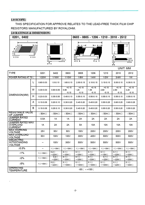
5.1 VOLTAGE RATING: RESISTORS SHALL HAVE A RATED DIRECT-CURRENT (DC) CONTINUOUS WORKING VOLTAGE OR AN APPROXIMATE SINE-WAVE ROOT-MEAN-SQUARE (RMS) ALTERNATING-CURRENT (AC) CONTINUOUS WORKING VOLTAGE AT COMMERCIAL-LINE FREQUENCY AND WAVEFORM CORRESPONDING TO THE POWER RATING, AS DETERMINED FROM THE FOLLOWING FORMULA:
34
392
58
698
82
127
11
226
35
402
59
715
83
130
12
232
36
412
60
732
84
133
13
237
37
422
61
750
85
137
14
243
38
432
62
768
86
140
15
249
39
442
63
787
87
143
16
255
40
45364ຫໍສະໝຸດ 80688147
17
261
41
464
65
825
EXAMPLE:
33000 → 33KΩ
(3) ±2%、±5%TOLERANCE: BELOW 10Ω SHOW AS FOLLOWING, READ ALPHABET”R” AS DECIMAL POINT. EXAMPLE:
0805自恢复保险丝

A.Features重要特性♦Smaller size saves board space and cost超小尺寸、节约空间和成本♦Resettable circuit protection自恢复保护、免维护♦Fast time-to-trip动作时间快♦Low resistance低内阻值♦Surface mount packaging for automated assembly贴片式封装,方便自动化生产♦Lead-free and compliant with the European Union RoHS Directive2002/95/EC 符合欧州ROHS无铅环保要求B.Application应用范围Polymer Resettable Fuse for over-current,over-temperature and short-circuit protection 可恢复保险丝用于过流、温度和线路短路保护♦Computer motherboards计算机主板♦IEEE1394PortsIEEE1394通讯接口♦USB hub,ports and peripheralsUSB交换机及外围设备♦Phones电话设备♦Data communication数据交换机♦Modems/Ethernet/LAN调制解调器/以太网C.General Description简要概述Polymer resettable fuse are made of polymeric PTC materials which is a matrix of自恢复保险丝是聚合物高分子材料通过特殊工艺而成,polymer containing dispersed conductive particles.Generally,the device has a very高分子粒子按一定的规律排列,自恢复保险丝器件有低内阻low resistance.If an over-current happened,as a response to the damage current,当电路中电流突然增大时,the resistance will immediately increase to very high,reducing the current of the器件将会在短时间内阻值升到高阻状态、高分子膨胀circuit to a safe value that the loading can carry.Once fault to the circuit is weed out从而起到减少过电流;and power is recuperated,the polymer will deflate itself,the device will reset and is 一旦故障排除后,高分子将会恢复正常规则排序。
0805封装尺寸0402封装尺寸0603封装尺寸1206封装尺寸(转载)-jia...
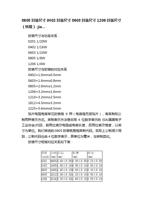
0805封装尺寸0402封装尺寸0603封装尺寸1206封装尺寸(转载)-jia...封装尺寸与功率关系:0201 1/20W0402 1/16W0603 1/10W0805 1/8W1206 1/4W封装尺寸与封装的对应关系0402=1.0mmx0.5mm0603=1.6mmx0.8mm0805=2.0mmx1.2mm1206=3.2mmx1.6mm1210=3.2mmx2.5mm1812=4.5mmx3.2mm2225=5.6mmx6.5mm贴片电阻电容常见封装有9种(电容指无级贴片),有英制和公制两种表示方式。
英制表示方法是采用4位数字表示的EIA(美国电子工业协会)代码,前两位表示电阻或电容长度,后两位表示宽度,以英寸为单位。
我们常说的0805封装就是指英制代码。
实际上公制很少用到,公制代码也由4位数字表示,其单位为毫米,与英制类似。
封装尺寸规格对应关系如下表:封装尺寸与功率有关通常如下:关于电容的封装除了上面的贴片封装外,对无极性电容,其封装模型还有RAD类型,例如“RAD-0.1”“RAD-0.2”等,后缀数字表示封装模型中两个焊盘间的距离,单位为英寸。
有极的电解电容的封装模型为RB类型,例如从“RB-.2/.4”到“RB-.5/.10”,其后缀的第一个数字表示封装模型中两个焊盘间的距离,第二个数字表示电容外形的尺寸,单位为也是英寸。
电阻:RES1,RES2,RES3,RES4;封装属性为axial系列无极性电容:cap;封装属性为RAD-0.1到rad-0.4电解电容:electroi;封装属性为rb.2/.4到rb.5/1.0电位器:pot1,pot2;封装属性为vr-1到vr-5二极管:封装属性为diode-0.4(小功率)diode-0.7(大功率)三极管:常见的封装属性为to-18(普通三极管)to-22(大功率三极管)to-3(大功率达林顿管)电源稳压块有78和79系列;78系列如7805,7812,7820等79系列有7905,7912,7920等常见的封装属性有to126h和to126v整流桥:BRIDGE1,BRIDGE2: 封装属性为D系列(D-44,D-37,D-46)电阻:AXIAL0.3-AXIAL0.7 其中0.4-0.7指电阻的长度,一般用AXIAL0.4瓷片电容:RAD0.1-RAD0.3。
自恢复保险丝规格书

Radial leaded devices Cured, flame retardant epoxy polymer insulating
material meets UL94 V-0 requirements Available in lead-free version Agency Recognition: UL、CSA、TUV
LP30 series
R-line devices
Product Dimensions
A
B
C
D
E
F
Lead
Part number
Max.
Max.
Typ.
Min.
Max.
Typ.
Style
Size(φ)
LP30-090F
6.0
13.8
5.1
7.6
3.0
0.9
1
0.6
LP30-110F
7.8
14.0
5.1
0.005
IH=Hold current: maximum current at which the device will not trip at 25℃ still air. IT=Trip current: minimum current at which the device will always trip at 25℃ still air.
Page 3 of 3
30min, at IH Vmax, Imax, 100cycles
Vmax, 24hours
Accept/Reject Criteria Rmin≤R≤Rmax
T≤maximum Time to Trip
自恢复保险丝选型指南

自恢复保险丝选型指南自恢复保险丝是一种重要的电气保护设备,主要用于在电路发生过载或短路时切断电流,以保护电器设备和电路的安全。
选择适合的自恢复保险丝类型对确保电路的正常运行至关重要。
本文将提供一个自恢复保险丝选型指南,帮助读者了解不同类型保险丝的特点和应用场景,以便根据实际需求选择合适的保险丝。
首先,我们需要了解什么是自恢复保险丝。
自恢复保险丝,也被称为PTC保险丝(正温度系数保险丝),是一种基于正温度系数(Positive Temperature Coefficient,PTC)效应的电阻材料制成的保险丝。
当电流通过保险丝时,保险丝的温度上升,电阻值随之增加,并限制电流的流动。
一旦过载或短路情况解除,保险丝会自动恢复到正常状态,电流继续流动。
因此,自恢复保险丝不需要更换,能够提供长时间的可靠保护。
1. 电流额定值(Current Rating):根据电路中的电流需求选择适当的电流额定值。
保险丝的额定电流应略高于电路中的最大工作电流,以确保保险丝能够快速切断电流,避免电路过载损坏。
2. 额定电压值(Voltage Rating):根据电路中的电压需求选择适当的电压额定值。
保险丝的额定电压应略高于电路中的最大工作电压,以确保保险丝能够安全切断电流,并避免电弧和火灾的发生。
3.尺寸和安装方式:根据电路的空间限制和安装需求选择适当的尺寸和安装方式。
自恢复保险丝通常可分为贴片式(SMD)和插件式两种安装方式。
贴片式保险丝适合于紧凑的电路板设计,而插件式保险丝则适用于传统的插件式电路板。
4. 响应时间(Time-to-Trip):响应时间是指保险丝从开始过载或短路发生到切断电流的时间。
根据系统的要求选择适当的响应时间。
一般来说,响应时间较短的保险丝能够更快地切断电流,但也可能对电路的正常工作造成干扰。
5. 温度特性(Temperature Coefficient):不同类型的自恢复保险丝的温度特性不同。
根据环境温度和电路工作温度范围选择适当的温度特性。
0805尺寸规格的说明
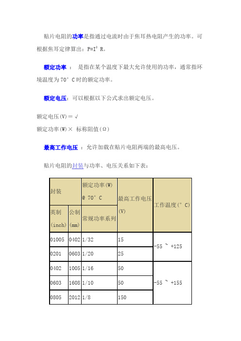
贴片电阻的功率是指通过电流时由于焦耳热电阻产生的功率。
可根据焦耳定律算出:P=I2 R。
额定功率:是指在某个温度下最大允许使用的功率,通常指环境温度为70°C时的额定功率。
额定电压:可以根据以下公式求出额定电压。
额定电压(V)=√额定功率(W)× 标称阻值(Ω)最高工作电压:允许加载在贴片电阻两端的最高电压。
贴片电阻的封装与功率、电压关系如下表:图1 (-55 ~+125)功率及环境温度降额曲线图图2 (-55 ~+155)功率及环境温度降额曲线图注意事项:•设计和使用贴片电阻时,最大功率不能超过其额定功率,否则会降低其可靠性。
•一般按额定功率的70%降额设计使用。
•也不能超过其最大工作电压,否则有击穿的危险。
•一般按最高工作电压的75%降额设计使用。
•当环境温度超过70°C,必须按照降额曲线图(图1,图2)降额使用。
我们俗称的封装是指英制。
规格书//电容规格书.pdf贴片电阻常见封装有9种,用两种尺寸代码来表示。
一种尺寸代码是由4位数字表示的EIA(美国电子工业协会)代码,前两位与后两位分别表示电阻的长与宽,以英寸为单位。
我们常说的0603封装就是指英制代码。
另一种是米制代码,也由4位数字表示,其单位为毫米。
下表列出贴片电阻封装英制和公制的关系及详细的尺寸:英制(inch ) 公制(mm)长(L)(mm)宽(W)(mm)高(t)(mm)a(mm)b(mm)02010603 0.60±0.050.30±0.050.23±0.050.10±0.050.15±0.0504021005 1.00±0.100.50±0.100.30±0.100.20±0.100.25±0.1006031608 1.60±0.150.80±0.150.40±0.100.30±0.200.30±0.2008052012 2.00±0.201.25±0.150.50±0.100.40±0.200.40±0.2012063216 3.20±0.201.60±0.150.55±0.100.50±0.200.50±0.201210 322 3.20±0. 2.50±0.0.55±0.0.50±0.0.50±0.Note:我们俗称的封装是指英制。
贴片压敏电阻0805封装参数型号规格书大全
UN Semiconductor Co., Ltd.
Revision December 18, 2013
3/5
@ UN Semiconductor Co., Ltd. 2013
MULTILAYER CHIP VARISTORS
UN0805-XXXH Series
Packaging Specification
hours, the change of varistor voltage shall be within 10%.
Damp Heat Load/ Humidity Load
The specimen should be subjected to 40℃,90 to 95%RH environment, and the maximum allowable voltage applied for 1000 hours, then stored at room temperature and humidity for one or two hours. The change of varistor voltage shall be within 10%.
machine. And a normal paper tape shall be connected in the head of taping for the operator handle.
type
0402 0603 0805 1206 1210 1812 2220 3220
A0 ±0.10
1.08
B0
K0
±0.10 ±0.10
1.88 1.04
T ±0.05 0.22
T2
D0
±0.05 +0.10
自恢复保险丝SMD0805封装参数型号规格书大全
The SMD0805Series PTC provides surface mount over-current protection for applications where space is at a premium and reset table protection is desired.◆RoHS compliant,Lead-Free and Halogen-Free ◆Fast time-to-trip◆Compact design saves board space ◆Agency recognition:UL ◆Low-profileAlmost anywhere there is a low voltage power supply,up to 16V and a load to be protected,including:◆Computer mother board,B hub ◆PDAs &Charger,Analog &digital line card ◆Digital cameras,Disk drivers,CD-ROMs ◆USB peripherals ◆Power ports◆General electronicsPartNumberIhold (A)I trip (A)V max (Vdc)I max (A)P dtyp.(W)Maximum TimeTo Trip ResistanceCurrent (A)Time (Sec.)R min (Ω)R max (Ω)SMD0805-0100.100.30151000.500.50 1.50 1.000 6.000SMD0805-0200.200.5091000.508.000.020.650 3.500SMD0805-0350.350.7561000.508.000.100.250 1.200SMD0805-0500.50 1.0061000.508.000.100.1500.085SMD0805-0750.75 1.506400.608.000.200.0900.385SMD0805-1001.01.9561000.608.000.300.0600.230I hold =Hold current:maximum current device will pass without tripping in 25°C still air.I trip =Trip current:minimum current at which the device will trip in 25°C still air.V max =Maximum voltage device can withstand without damage at rated current (I max )I max =Maximum fault current device can withstand without damage at rated voltage (V max )P dtyp.=Power dissipated from device when in the tripped state at 25°C still air.R min =Minimum resistance of device in initial (un-soldered)state.R max =Maximum resistance of device in initial (un-soldered)state.R 1max =Maximum resistance of device at 25°C measured one hour after tripping.Caution:Operation beyond the specified rating may result in damage and possible arcing and flame.Part NumberAmbient Operation Temperature-40°C-20°C0°C25°C40°C 50°C 60°C 70°C 85°CHold Current (A)SMD0805-0100.140.120.110.10.80.70.60.50.3SMD0805-0200.280.250.230.200.170.140.120.100.07SMD0805-0350.470.440.390.350.300.270.240.200.14SMD0805-0500.680.620.550.500.400.370.330.290.23SMD0805-075 1.000.900.790.750.630.570.530.410.34SMD0805-1001.351.251.151.000.820.740.650.550.42A=SMD0805-010B=SMD0805-020C=SMD0805-035D=SMD0805-050E=SMD0805-075F=SMD0805-100Part MarkingXPart Identification1Example1= SMD0805-010 2= SMD0805-020 3= SMD0805-035 5= SMD0805-050 7= SMD0805-075 0= SMD0805-100Profile FeaturePb-Free Assembly Average Ramp-Up Rate (T S max to T P ) 3°C/second max. Preheat :Temperature Min (T S min) Temperature Max (T S max) Time (T S min to T S max) 150°C 200°C60-180 seconds Time maintained above: Temperature(TL) Time (tL)217°C60-150 seconds Peak/Classification Temperature(T P ): 260°C Time within 5°C of actual peak: Temperature20-40 seconds Ramp-down Rate:6°C/ second max. Time 25°C to Peak Temperature8 minutes max.Note: All temperatures refer to of the package, measured on the package body surface.Solder reflowDue to “Lead Free ” nature, Temperature and Dwelling time for the soldering zone is higher than those for Regular. This may cause damage to other components.1.Recommended max past thickness > 0.25mm.2.Devices can be cleaned using standard methods and aqueous solvent.3.Rework use standard industry practices.4.Storage Environment : < 30℃/ 60%RHCaution:1.If reflow temperatures exceed the recommended profile, devices may not meet the performance requirements.2.Devices are not designed to be wave soldered to the bottom side of the board.Soldering ParametersRamp-downPreheatCritical Zone T L to T PTime to peak temperature(t 25℃ to peak)T PT L T S(max)T S(min)25T e m p e r a t u r eRamp-upTimeA B C DeviceNominalNominal Nominal 0805 Series1.201.001.50The dimension in the table below provide the recommended pad layout for each SMD0805 devicePart Numbering Pa c k ag ingPad Layouts Unit: mmTerminal pad material Pure TinSoldering CharacteristicsMeets EIA specification RS 186-9E, ANSI/J-std-002 Category 3Material Specifications010SMD0805Product nameSMD :surface mount deviceHold Current 0.10ATape & Reel Quantity5,000 pcs/reelABCDEPart NumberMin.Max. Min. Max. Min. Max. Min. Max. Min. Max. SMD0805-010 2.00 2.20 1.20 1.50 0.50 1.00 0.20 0.60 0.10 0.45 SMD0805-020 2.00 2.20 1.20 1.50 0.45 1.00 0.20 0.60 0.10 0.45 SMD0805-035 2.00 2.20 1.20 1.50 0.45 1.00 0.20 0.60 0.10 0.45 SMD0805-050 2.00 2.20 1.20 1.50 0.30 0.60 0.20 0.60 0.10 0.45 SMD0805-075 2.00 2.20 1.20 1.50 0.40 1.00 0.20 0.60 0.10 0.45 SMD0805-1002.002.201.201.500.501.100.200.600.100.45Dimensions Unit: mmu Operation beyond the specified maximum ratings or improper use may result in damage and possible electrical arcing and/or flame.u PPTC device are intended for occasional over-current protection. Application for repeated over-current condition and/or prolonged trip are not anticipated.uAvoid contact of PPTC device with chemical solvent. Prolonged contact will damage the device performance.WarningTape and Reel SpecificationsDirection of Feed0.33 (8.4)0.512(13.0)Arbor Hole Diameter7.0 (177.8)0.212 (5.4)0.157 (4.0) 0.059(1.5)Diameter Cover tape0.314 (8.0)0.157 (4.0)Dimensions are in inches(and millimeters)。
贴片保险丝
型号额定电压 额定电流外型尺寸 通过认证 资料下载2920SMD 自复保险丝15~60V0.3~3.0A7.3 ×5.0mmUL TUVPtc2920-1.PDF29 20 英寸 1812SMD 自复保险丝10~40V0.1~2.6A4.6 ×3.0mmUL TUVPTC1812-1.PDF PTC1812-2.PDF18 12 英寸 1206SMD 自复保险丝6V0.35~1.5A3.2×1.6mmUL TUV PTC1206-1.PDF PTC1206-2.PDF12 06 英寸0805SMD 自复保险丝6~15V0.1~0.75A2.0×1.2mmUL TUVPTC0805-1.PDF PTC0805-2.PDF系列外型尺寸1206 系列贴片保险丝3.2*1.6mm 0.12*0.06 英寸0603 系列贴片保险丝 1.6*0.8mm 0.06*0.03 英寸0402 系列贴片保险丝 1.0*0.5mm 0.01*0.005 英寸2410 系列贴片保险丝 6.8*2.7mm 0.24*0.10 英寸型号额定电压额定电流外型尺寸(mm)通过认证资料下载20N 速断型250V/125V 0.1∽20AΦ2.7*7.2 UL/CSA/PSE20N.pdf20T.pdf 20T 延时型250V/125V0.1∽7.0AΦ2.7*7.2 UL/CSA/PSEMCR.pdf MCR 速断型125V0.062∽10AΦ3.1*7.5UL/CSAR251 速断型125V0.062∽15AΦ2.4*7.2 UL/CSA r251-253.pdf型号额定电压额定电流外型尺寸(mm)通过认证资料下载SR5 圆柱型250V 1∽5A Φ8.4*7.6 UR/VDE/CCC SR5.pdfSS5.pdf SS5 方型250V1∽5A Φ8.6*7.6*4 UR/CCCmet.pdf MET 圆柱型250V0.04∽6.3AΦ8.4*7.6UR/VDE/CCCMST 方型250V0.04∽6.3AΦ8.6*7.6*4 UR/VDE/CCC mst.pdfU30系列自恢复保险丝 耐压 30VG16系列自恢复保险丝耐压 16VS 系列自恢复保险丝 耐压 6-16V BR 系列自恢复保险丝 耐压 125V R250系列自恢复保险丝 耐压 250V原理说明 参数说明:保持电流(Ih ):25℃静止空气环境中不触发电阻突越的最高电流。
贴片保险丝
F0603-1.0A
H
1.00
32
50A
0.252
0.0150
F0603-1.5A
K
1.50
32
50A
0.108
0.0365
F0603-2.0A
N
2.00
32
50A
0.058
0.0595
F0603-2.5A
O
2.50
32
50A
0.043
0.1222
F0603-3.0A
P
3.00
32
50A
0.041
1.5267
S1206-3.5A
R
3.50
32
50A
0.035
1.5212
S1206-4.0A
S
4.00
32
35A
0.027
2.5356
S1206-5.0A
T
5.00
32
35A
0.019
3.3999
S1206-6.0A
6
6.00
32
35A
0.015
5.7505
S1206-7.0A
U
7.00
Model
型号
Ih
It
Trip Time
Vmax
Imax
Pdmax
Resistance
A
A
A
S
V
A
W
Rmin(W)
Rtyp(W)
Rmax(W)
0805-010-15
0.10
0.30
0.5
1.50
15.0
100
0.5
1.000
- 1、下载文档前请自行甄别文档内容的完整性,平台不提供额外的编辑、内容补充、找答案等附加服务。
- 2、"仅部分预览"的文档,不可在线预览部分如存在完整性等问题,可反馈申请退款(可完整预览的文档不适用该条件!)。
- 3、如文档侵犯您的权益,请联系客服反馈,我们会尽快为您处理(人工客服工作时间:9:00-18:30)。
(a) RoHS Compliant & Halogen Free
(b) Applications: All high-density boards
(c) Product Features: Small surface mountable, Solid state, Faster time to trip than
standard SMD devices, Lower resistance than standard SMD devices (d) Operation Current: 0.10A~1.10A (e) Maximum Voltage: 6V~24V DC
(f) Temperature Range : -40℃ to 85℃
2. Agency Recognition
UL : File No. E211981TÜV: File No. R50090556
3. Electrical Characteristics (23℃)
H I T =Trip current-minimum current at which the device will always trip at 23℃ still air. V MAX =Maximum voltage device can withstand without damage at it rated current.(I MAX )
I MAX = Maximum fault current device can withstand without damage at rated voltage (V MAX ).
Pd=Typical power dissipated-type amount of power dissipated by the device when in the tripped state in 23℃ still air environment. R MIN =Minimum device resistance at 23℃ prior to tripping.
R 1MAX =Maximum device resistance at 23℃ measured 1 hour after tripping or reflow soldering of 260℃ for 20 seconds. Termination pad characteristics
Termination pad materials: Pure Tin
4.
FSMD Product Dimensions (Millimeters)
6. Typical Time-To-Trip at 23℃
T
i
m e -t o -t r i p (S )
7. Material Specification
Terminal pad material: Pure Tin
Soldering characteristics: Meets EIA specification RS 186-9E, ANSI/J-std-002 Category 3
8. Part Numbering and Marking System
Part Numbering System Part Marking System
S M D □ □ □ - □ □ - 0805 F □
Warning: electrical arcing and/or flame.
-PPTC device are intended for occasional overcurrent protection. Application for repeated overcurrent condition and/or prolonged trip are not anticipated. 甲、 -Avoid contact of PPTC device with chemical solvent. Prolonged contact will damage the device
performance. A = SMD010-0805 / SMD010-24-0805 B = SMD020-0805 C = SMD035-0805 D = SMD050-0805 / SMD050-9-0805 E = SMD075-0805 F = SMD100-0805 G= SMD110-0805
Current Rating Part Identification Logo Example Voltage Rating
9. Pad Layouts 、Solder Reflow and Rework Recommendations
The dimension in the table below provide the recommended pad layout for each SMD 0805 device
Note 1: All temperatures refer to of the package,
measured on the package body surface.
Reflow Profile。