半导体材料第6章III-V族化合物半导体的外延生长课后答案
半导体材料实验课后思考题答案
半导体材料实验课后思考题答案一、单色X射线衍射法晶体定向实验原理:如果用一固定波长的X射线(或称单色X 射线)入射到一块晶体上,要使其能在某晶面上产生衍射,则必须使晶体的位置能连续改变,使欲衍射晶面的放置位置(即θ角)满足布拉格方程。
对不同结构的晶体和不同的晶面,其衍射线所出现的位置不同,我们根据衍射线所发现的位置就能确定出晶体的取向。
根据布拉格方程,当波长为λ的X射线以θ角入射到晶体上,若满足2dsinθ=nλ,X射线就会在晶面间距为d的一族平行晶面上产生衍射。
2、用DQ-3型定向仪应注意哪些?b.松开探测器支架紧固手钮,将探测器支架旋转到与被测样品所对应的角度上,然后将紧固手钮拧紧;d.调节“计数率”旋钮在中间位置,调节“调零”旋钮使μA 率表指针在零附近;f.调节mA 旋钮在适当位置(通常使用在2mA 以下);1)不进行测量时,请随时关上X光光闸;2)当要暂停操作时,请关高压,但不要经常关低压,断电将会使已确定显示角度丢失;3)当工作结束时,应关闭X光光闸,关断高压,将显示器的角度输入到数字开关,关断电源。
4)mA调节旋钮,用来改变X光管的管电流,可以根据被测样品选择适当的mA值,在满足使用的条件下,应尽量选择低mA,一般在 2mA以下;5)计数率旋钮,在探测器接受 X 射线的情况下,用来调节微安数率率表计数率的大小,应根据需要选择在合适的位置,在满足要求的条件下,应尽量选择小一点,通常指到80格。
计数率调节过大会使稳定性变差,在这种情况下,应通过提高mA来增加 X射线的强度;6)调零旋钮,在只开低压的情况下,用此旋钮调节微安数率率表指针在0-20格附近;7)时间常数旋钮,分为 1,2,3 档,通常被设置在 2 档,在微安数率率表指针摆动较大时,应放在3档的位置上(在这种情况下,因μA率表的跟随特性减慢,一定要缓慢的转动测角仪轮)。
角度显示器的作用:每次开机时都要用标准样片校对一次。
3、X 方向偏角α,其原因如下:假定基准平面与“0”位偏差为δ,待测晶片沿X 方向与表面的偏差为α,则调整θ角使衍射强度出现极大时的θ角读数θ1=θ-δ+α,θ2=θ-δ-α,(θ1-θ2)/2=[(θ-δ+α)-(θ-δ-α)]/2=2α/2=α即取二次测量θ角读数之差的二分之一为偏离角的测量值时。
半导体物理课后习题答案(精)

第一章习题1.设晶格常数为a的一维晶格,导带极小值附近能量Ec(k)和价带极大值附近能量EV(k)分别为:h2k2h2(k-k1)2h2k213h2k2Ec= +,EV(k)=-3m0m06m0m0m0为电子惯性质量,k1=(1)禁带宽度;(2)导带底电子有效质量;(3)价带顶电子有效质量;(4)价带顶电子跃迁到导带底时准动量的变化解:(1)导带:2 2k2 2(k-k1)由+=03m0m03k14d2Ec2 22 28 22=+=>03m0m03m0dk得:k=所以:在k=价带:dEV6 2k=-=0得k=0dkm0d2EV6 2又因为=-<0,所以k=0处,EV取极大值2m0dk2k123=0.64eV 因此:Eg=EC(k1)-EV(0)=412m02=2dECdk23m0 8πa,a=0.314nm。
试求: 3k处,Ec取极小值4 (2)m*nC=3k=k14(3)m*nV 2=2dEVdk2=-k=01m06(4)准动量的定义:p= k所以:∆p=( k)3k=k14 3-( k)k=0= k1-0=7.95⨯10-25N/s42. 晶格常数为0.25nm的一维晶格,当外加102V/m,107 V/m的电场时,试分别计算电子自能带底运动到能带顶所需的时间。
解:根据:f=qE=h(0-∆t1=-1.6⨯10∆k ∆k 得∆t= ∆t-qEπa)⨯10)=8.27⨯10-13s2-19=8.27⨯10-8s (0-∆t2=π-1.6⨯10-19⨯107第三章习题和答案100π 21. 计算能量在E=Ec到E=EC+ 之间单位体积中的量子态数。
*22mLn31*2V(2mng(E)=(E-EC)2解232πdZ=g(E)dEdZ 单位体积内的量子态数Z0=V22100π 100h Ec+Ec+32mnl8mnl1*2(2mn1V Z0=g(E)dE=⎰(E-EC)2dE23⎰VEC2π EC 23100h*2 =V(2mn2(E-E)Ec+8m*L2Cn32π2 3Ecπ =10003L32. 试证明实际硅、锗中导带底附近状态密度公式为式(3-6)。
半导体材料第7章III-V族化合物的外延生长课后答案

第7章III-V族化合物的外延生长1、解释:①*MOVPE:金属有机物气相外延生长。
②*MBE:分子束外延生长。
(超高真空条件下,用分子束或原子束输运源进行外延生长)③CBE:化学束外延生长。
④ALE:原子层外延。
(MLE—分子层外延)⑤二步外延法:以蓝宝石为衬底,先用MOPVE法,在550℃左右,先生长20~25nm厚的GaN缓冲层,然后升温到1030 ℃,接着生长GaN外延层,称为二步外延法。
⑥双气流MOVPE:用二组输入反应室的气路。
一路为主气路,沿与衬底平行的方向输入反应气体。
另一路为副气路,以高速度在垂直于衬底方向输入H2和N2混合气体。
副气路作用是改变主气流流向和抑制生长GaN时的热对流。
从而生长了具有高迁移率的CaN单晶层。
2、依据相图, LPE生长GaAs时说明如何从A点开始外延生长。
答:Ga溶液组分为C L1,当温度T=T A时,他与GaAs衬底接触,此时A点处于液相区,故它将溶掉GaAs衬底。
GaAs衬底被溶解后,溶液中As量增大,A点朝右移动至A’后,GaAs才停止溶解,如组分C L1的Ga溶液在温度T B时与GaAs接触,这时溶液为饱和态,GaAs将不溶解。
降温后溶液变成过饱和,这时GaAs将析出并沉积在GaAs衬底上进行外延生长。
3、为什么从70年代初就对GaN开展了研究工作但一直进展缓慢?答:GaN的熔点约为2800℃,在这个温度下氮的蒸汽压可达 4.5×10E9Pa。
即使在1200-1500℃温度范围内生长,氮的压力仍然在1.5×10E9Pa。
由于GaN较高的离解压,很难得到大尺寸的 GaN体单晶材料。
并且N在Ga溶液中的溶解度低于1%,因此很难生长体单晶。
由于得不到GaN衬底材料,所以GaN只能进行异质外延生长。
由于存在较大晶格失配和热失配,造成的缺陷较多,限制了器件性能的提高。
()4、在生长III-V族化合物时指出MBE、MOVPE和 CBE法使用的III族源及各自的生长机理。
半导体器件物理第6章习题及答案
第六章 金属-氧化物-半导体场效应晶体管6-3.在受主浓度为31610-cm 的P 型硅衬底上的理想MOS 电容具有0.1um 厚度的氧化层,40=K ,在下列条件下电容值为若干?(a )V V G 2+=和Hz f 1=,(b ) VV G 20=和Hz f 1=,(c )V V G 20+=和MHz f 1=。
解答: (1)V V G 2+=,Hz f 1= 由 si BTH C Q V ψ+-=014830004048.8510 3.5410(/)0.110K C F cm x ε----⨯⨯===⨯⨯ )(70.0105.110ln 026.02ln 221016V n N V i a T f si =⨯⨯===φψ si a s dm a B qN k x qN Q ψε02-=-=7.010106.110854.8122161914⨯⨯⨯⨯⨯⨯⨯-=-- )/(1088.428cm C -⨯-= 则 )(08.270.01054.31088.4880V C Q V si B TH=+⨯⨯=+-=--ψTH G V V < ,则21020000)21(εs a G sSk qN V C C C C C C C +=+=21141619168)1085.81210106.121054.321(1054.3---⨯⨯⨯⨯⨯⨯⨯⨯+⨯=)/(1078.128cm F -⨯=b) V V G 20=,Hz f 1=G TH V V >,低频)/(1054.3280cm F C C -⨯==∴c)V V G 20+=,MHz f 1=G TH V V >,因为高频,总电容为0C 与S C 串联820min 3.4810(/)s s s dmk C C F cm x ε-=====⨯则 )/(1075.1280cm F C C C C C s s -⨯=+=6-4.采用叠加法证明当氧化层中电荷分布为)(x ρ时,相应的平带电压变化可用下式表示:()x FBqx x V dx C x ρ∆=-⎰解答:如右图所示, 消除电荷电荷片dx x q )(ρ的影响所需平带电压:000000)()()()(C x dx x xq x x x k dx x q x C dx x q dV FBρερρ-=-=-=由 00x →积分:()x FBq x x V dx C x ρ∆=-⎰6-6.利用习题6-3中的结果对下列情形进行比较。
半导体课后答案

F1
2
( 0.0195) 0.026
2
2.8 1019
[1
2 exp( 0.0195)] 0.026
F1
2
( 0.0195) 0.026
6.6 1019 (cm 3 )
其中 F1 (0.75) 0.4
2
第四章
1. 当 E-EF 分别为 kT、4kT、7kT,用费米分布和玻尔兹曼分布分别计算分布概率,并对结 果进行讨论。
EC 0T
)
2
2.8 1019
F1
2
(
0.026 0.026
)
9.5
1018
(cm3
)
作业布置
1.教材 p.162 第 15 题。
补充作业: 1.掺磷的 n 型硅,已知磷的电离能为 0.044eV,求室温下杂质一半电离时费米能级的位置 和磷的浓度。 [解]n 型硅,△ED=0.044eV,依题意得:
4.55 105 cm3
EFn EFp
(2)光照产生非平衡载流子,稳态时 np ni 2e k0T
又 np (n 0 n)(p0 p) n0p0 n 0p p0p p2 (n p)
EFn EFp
由上两式得, p 2 (n0 p0 )p ni 2 (e k0T 1)
EFn EFp
又∵在室温下,故此 n 型 Si 应为高掺杂,而且已经简并了。
∵ ED
EC
ED
0.039eV , EC
EF
EC
EC
ED 2
0.0195 0.052 2k0T
即 0 EC EF 2 ;故此 n 型 Si 应为弱简并情况。 k0T∴ 0nDND
1 2 exp( EF
半导体课后答案
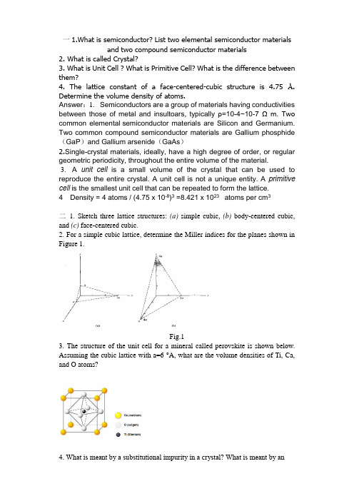
一1.What is semiconductor? List two elemental semiconductor materials and two compound semiconductor materials2. What is called Crystal?3. What is Unit Cell ? What is Primitive Cell? What is the difference between them?4. The lattice constant of a face-centered-cubic structure is 4.75 Å. Determine the volume density of atoms.Answer:1. Semiconductors are a group of materials having conductivities between those of metal and insultoars, typically ρ=10-4~10-7 Ω m. Two common elemental semiconductor materials are Silicon and Germanium. Two common compound semiconductor materials are Gallium phosphide (GaP)and Gallium arsenide(GaAs)2.Single-crystal materials, ideally, have a high degree of order, or regular geometric periodicity, throughout the entire volume of the material.3. A unit cell is a small volume of the crystal that can be used to reproduce the entire crystal. A unit cell is not a unique entity. A primitive cell is the smallest unit cell that can be repeated to form the lattice.4 Density = 4 atoms / (4.75 x 10⁻⁸)3 =8.421 x 10²³atoms per cm3二1. Sketch three lattice structures: (a) simple cubic, (b) body-centered cubic, and (c) face-centered cubic.2. For a simple cubic lattice, determine the Miller indices for the planes shown in Figure 1.Fig.13. The structure of the unit cell for a mineral called perovskite is shown below. Assuming the cubic lattice with a=6 °A, what are the volume densities of Ti, Ca, and O atoms?4. What is meant by a substitutional impurity in a crystal? What is meant by anintcrstilial impurity?2. left:(313) ; right:(121)3. solution: Density (Ca)= 881⨯atoms / a 3 = 4.63 x 10²¹ atoms per cm 3 Density (O)=216⨯ atoms / a 3 =1.39 x 10²² atoms per cm 3 Density (Ti)=1/a 3 = 4.63 x 10²¹ atoms per cm 3三 1. Ultraviolet light (紫外光) of wavelength 150nm falls on a chromium [/kr əʊmi:əm] (铬Cr) electrode(电极). Calculate the maximum kinetic energy and the corresponding velocity of the photoelectrons (the work function of chromium is4.37eV).2. Calculate the photon energies for the following types of electromagnetic radiation: (a) a 600kHz radio wave; (b) the 500nm (wavelength of) green light; (c) a 0.1 nm (wavelength of) X-rays.1、Solution: using the equation of the photoelectric effect, it is convenient to express the energy in electron volts. The photon energy isSolution:(a) for the radio wave, we can use the Planck-Einstein law directly(b) The light wave is specified by wavelength, we can use the law explained in wavelength:四 1 Determine the energy of a photon having wavelengths of (a) λ = 10,000Ǻ and (b) λ= 10Ǻ.2 (a) Find the momentum and energy of a particle with mass of 5 x10-31 kg and a de Broglie wavelength of 180Ǻ. (b) An electron has a kinetic energy of 20 meV . Determine the de Broglie wavelength.eV Hz s eV h E 93151048.21060010136.4--⨯=⨯⨯⋅⨯==ν1、(a) 1.99 x10⁻¹⁹J or 1.24eV. (b) 1.99 x10⁻¹⁶J or 1.24x10³eV2、(a) p=3.68 x10⁻²⁶kgm/s, E=1.35 x10⁻²¹J or 8.46 x10⁻³eV. (b) p=7.64 x10⁻²⁶kgm/s , λ= 86.7Ǻ五E2.5 The width of the infinite potential well in Example 2.3 is doubled to 10Ǻ. Calculatethe first three energy levels in terms of electron volts for an electron.E2.6 The lowest energy of a particle in an infinite potential well with a width of 100 Ǻ is0.025 eV. What is the mass of the particle?1、Ans. 0.376eV, 1.50eV, 3.38eV2、Ans. 1.37X10⁻³¹kg六1. What is the Kronig-Penney model ?2. Discuss the concept of allowed and forbidden energy bands in a single crystal qualitatively with your classmate.3. Discuss the splitting of energy bands in silicon with your classmate.4. (a) If 2X10¹⁶boron atoms per cm3are added to silicon as a substitutional impurity, determine what percentage of the silicon atoms and displayed in the single crystal lattice. (b) repeat part (a) for 1015 boron atoms per cm3. (课本P45)5. If 2X10¹⁵ gold atoms per cm3 are added to silicon as a substitutional impurity and are distributed uniformly throughout the semiconductor, determine the distance between gold atoms in terms of the silicon lattice constant. (Assume the gold atoms are distributed in a rectangular or cubic array.) (课本P45)七3.1Consider Figure 3.4b. which shows the energy-band splitting of silicon. Ifthe equilibrium lattice spacing were to change by a small amount. discusshow you would expect the electrical properties of silicon to change.Determine at what point the material would behave like an insulator or likea metal.3.2Show that Equations (3.4) and (3.6) are derived from Schrodinger's waveequation. using the fom~o f solution given by Equation (3.3).3.3Show that Equations (3.9) and (3.10) are solutions of the differentialequations given by Equations (3.4) and (3.8). respectively.3.4 Show that Equations (3.12) (3.14), (3.16). and (3.18) rcsult from theboundary conditions in the Kronig-Penney model.这四道题在课本第98页. 八For the electron near the top of the allowed energy band (see Figure 3.16b), show that it behaves as if it has a negative mass.(Refer to textbook pp77-78)2. p99,3.13-3.153. p45, E2.10 (selective)九Answer the questions:1. What is effective mass?2. What is a direct bandgap semiconductor? What is an indirect bandgap semiconductor?3. What is the meaning of the density of states function?4. What was the mathematical model used in deriving the density of states function?5. In general, what is the relation between density of states and energy? Problems:P1003.20, 3.22十3.13 m*(A)<m*(B)3.15 A, B: velocity =-x : C, D: velocity = +x;B. C: positive mass; A, D: negative mass19.3 Å十一Answer the questions1. In general, what is the relation between density of states and energy?2. What is the meaning of the Fermi-Dirac probability function?3. What is the Fermi energy?Problem:1.3P85, Example 3.32. Consider the density of states for a free electron given by Equation (3.69). Calculate the density of states per unit volume with energies between 0 and 2eV.3. To determine the possible number of ways of realizing a particular distribution. Let gi = 10 and Ni =8.4. Calculate the temperature at which there is a 10-6 probability that an energy state 0.55 eV above the Fermi energy level is occupied by an electron.十二Questions:1. Assuming the Boltzmann approximation applies, write the equations for n0 and p0 in terms of the Fermi energy.2. What is the value of the intrinsic carrier concentration in silicon at T = 300 K?3. Under what condition would the intrinsic Fermi level be at the midgap energy? Problems:P148,4.1, 4.2, 4.8, 4.12十三Questions:1. What is intrinsic semiconductor? What is extrinsic semiconductor? Why the extrinsic semiconductor is more useful than the intrinsic semiconductor?2. What is ionization energy? Why the resistance of the extrinsic semiconductor is quite sensitive to doping?Problems:1. Calculate the ionization energy of the hydrogen atom using Bohr theory.(-13.6eV)2. Calculate the ionization energy of the donor electron in silicon using Bohr theory. (for silicon, =1.17, =0.26). (-25.8meV)十四 P147, review questions, 7,8,10,11P149, 4.19, 4.21r *0/m m。
半导体物理MS接触习题参考答案

q 2
以空穴为例,空穴能量为:
E ( x) qs ( x) q2 16 Si x
势垒降低后的图如下所示:
(C) 如果在 M/S 界面半导体 Si 禁带中距价带 1/3Eg 的位置存在无穷大的界面态密 度,则费米能级被钉扎(pinned)在距价带 1/3Eg 处,势垒高度满足:
电中性条件:
din dx
x xn
dip dx
x xp
0
qNd xn qNa x p ,得
解泊松方程得:
xn N a xp Nd
qN d ( x ) ( x xn ) 2 in ( xn ) ( xn x 0) in 2 n ip ( x) qN a ( x x p ) 2 in ( x p ) (0 x x p ) 2 p
泊松方程:
qN d qN a
( xn x 0) (0 x x p )
d 2in qN d 2 n dx 2 d ip qN a dx 2 p
( xn x 0) (0 x x p )
在 x xn 和 x x p 处电场为零,即:
则:
qN d 2 in in ( xn ) in (0) 2 xn n ip in (0) in ( x p ) qN a x p 2 2 p ( xn x 0) (0 x x p )
qN d 2 x xn p N a p in 2 n n 有: ip qN a x 2 x p n N d n p 2 p
半导体材料第9讲-III-V族化合物半导体的外延生长2

III-V族化合物半导体的外延生长
MOVPE法生长GaN
GaN的熔点约为2800℃,在这个温度下氮的蒸气压可达 4.5×10⁹Pa.即使在1200~1500℃温度范围内生长,氮 的压力仍然为1.5×10⁹pa,并且N在Ga中的溶解度低于1 %,因此,很难生长体单晶。
由于得不到GaN衬底材料,所以GaN只能进行异质外延生 长。目前作为实用的衬底材料的有SiC、蓝宝石等,也在 寻找新的衬底材料,如ZnO、Si、GaAs及某些锂盐等。 现在用于生长制备高亮度蓝色发光二极管所需GaN系材料 的方法是MOVPE,,
原料:以蓝宝石(0001)为衬底,NH3和TMG为N 和Ga源,H2为输运气体。
晶格失配:由于GaN和衬底之间的失配大到15.4 %,为此先用MOVPE法,在550℃左右,在衬底 上先生长一层20~25nm厚的GaN的缓冲层,然 后升温至1030℃,接着生长GaN外延层。
晶格失配
在异质外延层和衬底或相邻的两个外延层之间, 如果存在晶格常数的差异,称之为晶格失配。 晶格失配率:
MBE的设备
MBE设备主要由真空系统、生长系统及监控系统等组成。
MBE生长系统 以不锈钢结构为主体,由三个真空室连接 而成,分别为衬底取放室、衬底存储传送室和生长室。
三个室之间用高真空阀门连结,各室都能独立地做到常 压和高真空转换而不影响其他室内的真空状态。这三个室均 与由标准机械泵、吸附泵、离子泵、液N2冷阱、钛升华泵等 构成的真空系统相连,以保证各室的真空度均可达到1×10⁸~1×10⁻⁹Pa,外延生长时,也能维持在10-7Pa的水平为了 获得超高真空,生长系统要进行烘烤,所以生长系统内的附 属机件应能承受200~250℃的高温,并且具有很高的气密性。
等。
- 1、下载文档前请自行甄别文档内容的完整性,平台不提供额外的编辑、内容补充、找答案等附加服务。
- 2、"仅部分预览"的文档,不可在线预览部分如存在完整性等问题,可反馈申请退款(可完整预览的文档不适用该条件!)。
- 3、如文档侵犯您的权益,请联系客服反馈,我们会尽快为您处理(人工客服工作时间:9:00-18:30)。
第六章III-V族化合物半导体的外延生长
1、缩写解释:
①*HB:水平布里奇曼法,又叫横拉法。
两温区HB法生长GaAs:低温区使As形成高压
As蒸汽,高温区使As蒸汽和Ga液反应生成GaAs溶液,然后由籽晶生成GaAs晶体。
②*LEC(LEP):液态密封法。
在高压炉内,将欲拉制的化合物材料盛于石英坩埚中,上
面覆盖一层透明而黏滞的惰性熔体,将整个化合物熔体密封起来,然后再在惰性熔体上充以一定压力的惰性气体,用此方法来抑制化合物材料的离解,用这种技术可以拉制GaAs、InP、GaP等的大直径单晶。
③SSD:合成溶质扩散法(synthesis solute diffusion)
④VCZ:蒸汽控制直拉技术。
⑤VGF:垂直梯度凝固法。
2、从*能带结构特点比较硅和GaAs在应用上的不同。
答:①室温下,Si的Eg=1.12ev,GaAs的Eg=1.43ev,禁带宽度大,GaAs半导体器件的工作温度范围比Si器件的工作范围要大。
②Si是间接带隙半导体材料,不可用作发光材料,而GaAs是直接带隙半导体材料,
可作为发光材料。
③GaAs具有双能谷能带结构,可以制作体效应微波二极管,而Si不能。
④GaAs的电子迁移率比Si大得多,有利于提高晶体管的高频性能。
3、解释作为间接带隙材料GaP为什么能成为可见光 LED的主要材料?
答:GaP的发光机理是激子复合发光,激子是价带中的电子向导带跃迁时,由于能量不够,受到价带中的空穴的库仑力的作用而停留在禁带中形成电子-空穴对,此为激
子。
由于等电子陷阱能级在k空间的扩展,在k=0附近通过直接跃迁,电子与空
穴复合,因此可以效率较高的发光。
而GaP的Eg=2.26ev,对应发光波长为550nm,所以作为间接带隙材料的CaP能成为可见光LED的主要材料。
4、详细说明三温区横拉法中温度选择的依据。
(T1=1250℃、T2=1100℃、T3=610℃)。
答:在三温区横拉法中,采用的是三温区横拉单晶炉改变炉温分布。
①T1=1250℃是使As蒸汽+Ga液在1250℃、P AS≈100kpa下可以生成GaAs,满足化
学计量比,生长条件是由GaAs相图得到的;
②T2=1100℃是因为在GaAs的合成与晶体生长时,在高温区将发生GaAs熔体中的
Ga与石英反应,4Ga(l)+SiO2=Si(s)+2Ga2O(g),在低温区有反
应,3Ga2O(g)+As4(g)=Ga2O3(s)+4GaAs(s)。
反应1引起的Si沾污受反应2小号Ga2O
而加强,但反应2与温度有关,温度升高能减弱消耗Ga2O的反应,从而抑制了反应
1中的Si生成。
T2=1100℃可以抑制低温反应的进行从而抑制Si(s)的生成,减少了
GaAs单晶中Si的沾污。
(*抑制沾污的反应机理)
③T3=610℃是As端的温度,此温度可形成100kPa的As蒸汽,提高了平衡蒸汽压,
正是生成GaAs所需要的蒸汽压。
5、GaAs成为继Si之后重要半导体材料的重要特征有哪些?
答:①直接带隙,光电材料;
②迁移率高,适于制作超高频超高速器件和电路;
③易于制成非掺杂半绝缘单晶,IC中不必作绝缘隔离层,简化IC,减少寄生电容,
提高集成度;
④Eg较大,可在较高温度下工作;
⑤抗辐射能力强;
⑥太阳电池,转换率比Si高;
⑦Gunn效应,新型功能器件.
6、补充:
①GaAs<100>方向上有双能谷能带结构。
室温下,电子处在主能谷中,很难跃迁到导带
能谷中去。
但电子在主能谷中有效质量较小,迁移率大,而在次能谷中,有效质量大,迁移率小且次能谷中的状态密度又比主能谷大,一旦外电场超过一定值,电子就可以由迁移率大的主能谷转移到迁移率小的次能谷,而出现电场增大电流减小的*负阻现象。
这是制作体效应微波二极管的基础。
②闪锌矿晶体的解理主要沿(110)面发生。
(极性对解理性的影响)
③GaAs体系图的解释 P142
④*III-V族化合物的极性对晶体的影响:解理性、表面腐蚀、晶体生长。
7、GaAs单晶中Si沾污的抑制:(不太重要)
答:①采用三温区横拉单晶炉改变炉温分布。
②降低合成GaAs及拉晶时高温区温度。
③压缩反应系统与GaAs熔体的体积比。
④向系统中加入O2、Ga2O3、As2O3,抑制反应1
⑤改变GaAs熔体与石英舟的接触状态。
8、*LEP液态密封法中所用覆盖剂应满足条件(老师没画)
答:1.密度小于拉制材料;
2.对熔体和坩埚在化学上必须是惰性的,而且熔体中溶解度小;
3.熔点低于被拉制材料熔点,且蒸汽压低,易去掉;
4.有较高纯度,熔融状态下透明。