DC降压转换器
1A降压型DC-DC转换器EL7536中文资料
E L7536单片1A步降调整器概述EL7536是带有内部补偿的同步集成FET 1A步降调整器。
它工作的输入电压范围为2.5V~5.5V,适用于3.3V,5V的电源,或锂离子电源。
输出可通过电阻分压器从外部设置,范围为0.8V~V IN。
EL7536的主要特点是PWM模式控制。
它的工作频率的典型值是1.4MHz。
其他特点还包括100ms的上电复位输出,小于1µA 的关机电流和过热保护。
EL7536是10引脚MSOP封装,所有零件只占用印刷电路板的一面,且整个转换器的面积小于0.15in2。
EL7536规定的工作温度范围为-40℃到+85℃。
订购信息表特点整个1A 转换器的覆盖面积小于0.15in2(0.97cm2)所有零件在PCB的一面最大高度为1.1mm MSOP10100ms的加电复位输出(POR)内部补偿电压模式控制器高达97%的效率<1µA的关机电流过流和过热保护无铅(依照RoHS)应用PDA和袖珍式PC电脑条形码识别器蜂窝式电话便携式测试设备锂离子电池供电设备小结构(SFP)模块管脚引出线和典型应用图极限参数(T A=25℃)对SGND的V IN,V DD和POR………………………………-0.3V至+6.5V对PGND的LX………………………………………… -0.3V至(V IN++0.3V)对SGND的RSI,EN,V O和FB………………………… -0.3V至(V IN++0.3V)对SGND的PGND…………………………………………… -0.3V至+0.3V输出峰值电流………………………………………………… 1.2A工作环境温度…………………………………………………-40℃至+85℃贮存温度……………………………………………………… –65℃至+150℃节点温度 (145)电气指标所有规格在V DD=V IN=V EN=3.3V,C1=C2=10μF,L=1.8μH,V O=1.8V的条件下,除非另有说明。
大电流dc-dc降压设计原理

大电流dc-dc降压设计原理大电流 DC-DC 降压设计原理大电流 DC-DC 降压转换器在各种电子系统中扮演着至关重要的角色,从便携式设备到工业电机控制。
它们将较高电压转换为较低电压,同时保持或增加电流容量。
以下是设计大电流 DC-DC 降压转换器的关键原理:功率器件选择选择合适的功率器件(开关管)对于确保转换器的效率和可靠性至关重要。
常见的选项包括 MOSFET(金属氧化物半导体场效应晶体管)和 IGBT(绝缘栅双极型晶体管)。
对于大电流应用,低导通电阻和低栅极电荷的功率 MOSFET 是理想的选择。
开关频率和电感值开关频率和电感值共同决定了转换器的尺寸、效率和纹波电流。
较高的开关频率通常会导致较小的电感值,但会增加开关损耗。
较低的开关频率需要更大的电感值,但会降低效率。
最佳值取决于负载电流、电压和纹波电流要求。
输入和输出电容输入和输出电容用于吸收电流纹波,从而平滑转换器输出电压。
电容值为开关频率、负载电流和纹波电流要求的函数。
电容的 ESR (等效串联电阻)也应尽可能低,以最大限度地减少损耗。
反馈回路反馈回路用于调节转换器的输出电压。
常见拓扑包括电压模式和电流模式。
电压模式控制通过比较输出电压与基准电压来调节占空比,而电流模式控制通过比较电感电流与基准电流来调节占空比。
同步整流同步整流技术可以提高转换器的效率,尤其是在大电流应用中。
通过使用低导通电阻的 MOSFET 作为整流器,而不是使用二极管,可以显著减少整流损耗。
散热大电流 DC-DC 降压转换器在大电流条件下运行,会产生大量热量。
因此,散热是至关重要的。
可以使用散热器、热垫和强制空气冷却来管理热量。
保护特性为了确保转换器的可靠性和安全性,应纳入多种保护特性。
这些包括过流保护、过压保护、欠压保护和短路保护。
布局和布线转换器的布局和布线对于性能至关重要。
应使用宽走线和低电感环路来最大限度地减少损耗和 EMI(电磁干扰)。
电容器和电感器应放置在靠近功率器件以最小化寄生效应。
buck芯片工作原理
Buck芯片工作原理一、概述Buck芯片是一种常见的DC-DC降压转换器,广泛应用于电子设备中。
本文将详细介绍Buck芯片的工作原理。
二、Buck芯片的基本原理Buck芯片通过控制开关管的导通和截止,实现输入电压的降压转换。
其基本原理如下:2.1 输入电压Buck芯片的输入电压通常由电池或电源提供,一般为直流电压。
输入电压的大小决定了输出电压的范围。
2.2 控制器Buck芯片内部的控制器负责监测输入电压和输出电压,并根据设定的参数控制开关管的导通和截止。
2.3 开关管Buck芯片内部包含一个开关管,用于控制输入电压的导通和截止。
开关管的导通和截止通过控制器的信号来实现。
2.4 电感和电容Buck芯片还包含一个电感和一个电容,用于实现电压的稳定输出。
电感在导通状态下储存能量,而电容则平滑输出电压。
2.5 输出电压Buck芯片的输出电压通过开关管的导通时间和频率来控制。
导通时间和频率越长,输出电压越接近输入电压。
三、Buck芯片的工作过程Buck芯片的工作过程可以分为导通状态和截止状态两个阶段。
3.1 导通状态在导通状态下,开关管导通,输入电压通过电感和开关管传递到电容上,同时电感储存能量。
此时输出电压较低。
3.2 截止状态在截止状态下,开关管截止,电容通过负载输出电压,同时电感释放储存的能量。
此时输出电压较高。
3.3 控制器调节Buck芯片的控制器不断监测输出电压,并通过控制开关管的导通时间和频率来调节输出电压。
如果输出电压过高,控制器会减少导通时间或降低频率,反之则增加导通时间或提高频率。
3.4 反馈回路Buck芯片的控制器通过反馈回路来实现输出电压的稳定。
反馈回路会将输出电压与设定的标准电压进行比较,并根据差异来调节开关管的导通时间和频率,以使输出电压保持在设定范围内。
四、Buck芯片的优缺点Buck芯片作为一种常见的降压转换器,具有以下优点和缺点:4.1 优点•高效率:Buck芯片的转换效率较高,能够将输入电压有效地转换为输出电压。
ltc1265高效降压dc dc转换器示波器用户手册说明书
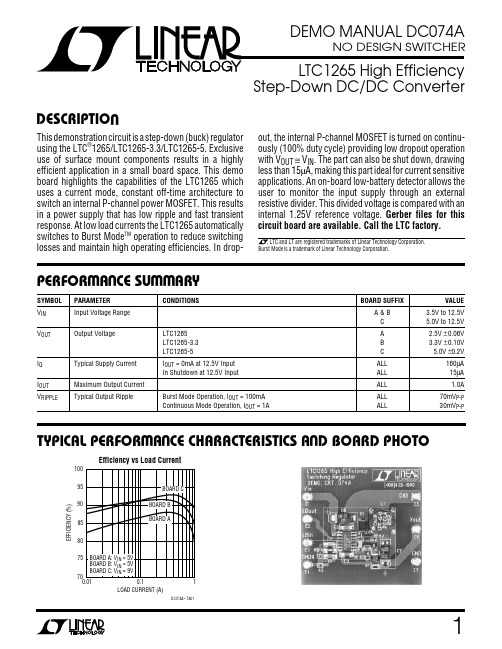
1SYMBOL PARAMETER CONDITIONSBOARD SUFFIXVALUE V IN Input Voltage Range A & B 3.5V to 12.5V C 5.0V to 12.5V V OUTOutput VoltageLTC1265A 2.5V ±0.06V LTC1265-3.3B 3.3V ±0.10V LTC1265-5C 5.0V ±0.2VI Q Typical Supply Current I OUT = 0mA at 12.5V Input ALL 160µA In Shutdown at 12.5V InputALL 15µA I OUT Maximum Output Current ALL 1.0A V RIPPLETypical Output RippleBurst Mode Operation, I OUT= 100mA ALL 70mV P-P Continuous Mode Operation, I OUT = 1A ALL30mVP-PStep-Down DC/DC ConverterDESCRIPTIOUThis demonstration circuit is a step-down (buck) regulator using the LTC ®1265/LTC1265-3.3/LTC1265-5. Exclusive use of surface mount components results in a highly efficient application in a small board space. This demo board highlights the capabilities of the LTC1265 which uses a current mode, constant off-time architecture to switch an internal P-channel power MOSFET. This results in a power supply that has low ripple and fast transient response. At low load currents the LTC1265 automatically switches to Burst Mode TM operation to reduce switching losses and maintain high operating efficiencies. In drop-out, the internal P-channel MOSFET is turned on continu-ously (100% duty cycle) providing low dropout operation with V OUT ≅ V IN . The part can also be shut down, drawing less than 15µA, making this part ideal for current sensitive applications. An on-board low-battery detector allows the user to monitor the input supply through an external resistive divider. This divided voltage is compared with an internal 1.25V reference voltage. Gerber files for this circuit board are available. Call the LTC factory.TYPICAL PERFOR A CE CHARACTERISTICS A D BOARD PHOTOU UW LOAD CURRENT (A)0.0170E F F I C I E N C Y (%)758085901000.11DC074A • TA0195Efficiency vs Load CurrentBurst Mode is a trademark of Linear Technology Corporation.PERFOR A CE SU ARYU W WW2DEMO MANUAL DC074ASYMBOL PARAMETERCONDITIONSBOARD SUFFIXVALUE ∆V OUTTypical Load Regulation0mA < I OUT < 1A, V IN = 10V A 30mV 0mA < I OUT < 1A, V IN = 10V B 50mV 0mA < I OUT < 1A, V IN = 10VC 70mV V IH Shutdown Pin High Minimum Voltage at Pin 10 for Device to Be in Shutdown ALL 1.2V V IL Shutdown Pin Low Maximum Voltage at Pin 10 for Device to Be in ActiveALL 0.6V I QLow-Battery Trip PointALL1.25 ±0.1VPERFOR A CE SU ARYU W WWS PACKAGE14-LEAD PLASTIC SOIC *ADJ OUTPUT VERSIONSPWR V IN V IN LB OUT LB IN C T I TH SENSE –SW PWR V IN PGND SGND SHDN NC (V FB *) SENSE +LTC1265CS LTC1265CS-3.3LTC1265CS-5V OUT µF LTC1265 LTC1265-3.3 LTC1265-5PACKAGE A D SCHE ATIC DIAGRA SU W WPARTS LISTREFERENCE DESIGNATOR QUANTITYPART NUMBER DESCRIPTIONVENDOR TELEPHONE C11VJ1206A392KXAT Cap, Mono Chip, 3900pF, 50V, 10%Vitramon (203) 268-6261C21VJ1206U103MXAT Cap, Mono Chip, 0.01µF, 25V, 10%Vitramon C31VJ1206U104MXXAT Cap, Mono Chip, 0.1µF, 25V, 10%Vitramon C41VJ1206A101KXAT Cap, Mono Chip, 100pF, 50V, 10%Vitramon C51VJ1206A181JXAT Cap, Mono Chip, 180pF, 50V, 5%: Board AVitramon VJ1206A151JXAT Cap, Mono Chip, 150pF, 50V, 5% : Board B & C C61593D686X0020E2W Tantalum Cap, 68µF, 20V, 20%Sprague (207) 324-4140C71593D107X0010D2W Tantalum Cap, 100µF, 10V, 20%Sprague D11MBRS130LT3Schottky DiodeMotorola (602) 244-3558L11LPT4545-200Inductor, 20µH : Board A & B Dale(605) 665-9301LPT4545-330Inductor, 33µH : Board CFigure 1.3DEMO MANUAL DC074APARTS LISTREFERENCE DESIGNATOR QUANTITY PART NUMBER DESCRIPTION VENDOR TELEPHONE R1 1WSL2010-0.10.1Ω 1% 0.5W Resistor Dale (605) 665-9301R2 1CRCW1206499J 499Ω 5% Chip Resistor Dale R3 1CRCW1206223J 22k 5% Chip Resistor Dale RFB1, RFB2 1CRCW1206343J 34k 5% Chip Resistor: Board A Dale U11LTC1265CS Board A IC LTC(408) 432-1900LTC1265CS-3.3Board B IC LTC1265CS-5Board C ICQUICK START GUIDEThis demonstration board is easy to set up to evaluate the performance of the LTC1265. Please follow the procedure outline below for proper operation.•Connect the input power supply to the V IN and GND terminals.•The LB OUT pin is a current sinking pin. When the LB IN pin goes below 1.25V the LB OUT pin will sink 1mA of current.•The LB IN pin is the low battery detector input pin.Normally, its input comes from the input voltagethrough a resistive divider network (see LOW BAT-TERY DETECTOR).•Connect the load between the V OUT and GND terminals.•Refer to Figure 4 for proper arrangement of measure-ment equipment setup•The SHDN pin is pulled down to ground by R3. To put the part in shutdown, connect a voltage greater than 1.2V to this pin.OPERATIOUcurrent limit and excellent line and load regulation. The constant off-time adds to this list simplicity (neither an oscillator nor ramp compensation are required), inherent 100% duty cycle in dropout, and constant inductor ripple current.Because the off-time is constant, the operating frequency changes with input voltage. For example, in an LTC1265-3.3 application the frequency will double when V IN is increased from 4.7V to 8V with V OUT at 3.3V. To maximize the efficiency over a wide current range, loss reducing circuit techniques must be carefully applied. Because of the MOSFET gate charge, switching the gate from V IN to ground ends up as additional input current from V IN ,decreasing efficiency. At low output currents this loss term dominates. This is the principal reason that the LTC1265 changes to Burst Mode operation as the output current drops.The circuit shown in Figure 1 operates from input voltages of 3.5V to 12.5V. For Board A, the output voltage is set to 2.5V by the resistive dividers, RFB1 and RFB2. For Board A and Board B, the circuit is optimized at input voltage of 5V while Board C is optimized at a 9V input voltage. For all boards, the LTC1265 is operating at a frequency of 200kHz when at their respective optimized input voltage and the LTC1265 is operating in continuous mode.This demonstration unit is intended for the evaluation of the LTC1265 switching regulator IC and was not designed for any other purposes.OPERATIONThe LTC1265 switching regulator uses the constant off-time, current mode architecture shown in Figure 2.Current mode operation was judged to be mandatory for its well-known advantages of clean start-up, accurate4DEMO MANUAL DC074AOPERATIOUThe continuous mode operation is as follows: the internal P-channel MOSFET switch is turned on at the end of the off-time and turned off when the inductor current has ramped up to the current comparator threshold. During the off-time the catch diode D1 turns on. At the end of the constant off-time, the P-channel MOSFET is again turned on and the cycle repeats.LTC1265 Burst Mode is automatically invoked when the current required by the load is less than the minimum current supplied by the continuous operation. During Burst Mode operation the output voltage is regulated via a hysteretic comparator which, when tripped, shuts down the MOSFET driver and much of the control circuitry to conserve DC supply current. From the time the compara-tor trips until the lower comparator threshold is reached,the load current is completely supplied by a charge stored in the output capacitor. When the output capacitor dis-charges to the lower threshold, the main loop again briefly turns on at a low current level to recharge the capacitor.This cycle repeats at a progressively slower rate as the output current is reduced.LOW-BATTERY DETECTORThe low-battery indicator senses the input voltage through an external resistive divider. This divided voltage connects to the (–) input of a voltage comparator (Pin 4) which is compared with a 1.25V reference voltage. With the current going into pin 4 being negligible, the following expression is used for setting the trip limit:V LB_TRIP = 1.251 +R4R3))Figure 2. LTC1265 Block DiagramFigure 3. Low-Battery ComparatorV FBADJUSTABLE VERSIONV DC074A • F035DEMO MANUAL DC074AOPERATIOUHOW TO MEASURE VOLTAGE REGULATIONWhen trying to measure voltage regulation remember that all measurements must be taken at the point of regulation. This point is where the LTC1265’s control loop looks for the information to keep the output voltage constant. This information occurs between Pin 7 and Pin 11 of the LTC1265. These points correspond to the output terminals of the demonstration board. Test leads should be attached to these terminals. Measurements should not be taken at the end of test leads at the load . Refer to Figure 4 for proper monitoring equipment configuration.This applies to line regulation (input to output voltage regulation) as well as load regulation tests. In doing line regulation tests always look at the input voltage across the input terminals.For the purposes of these tests the demonstration circuit should be fed from a regulated DC bench supply, so additional variation on the DC input does not add an error to the regulation measurements.The technique used to measure the ripple is also impor-tant. Here is a list of things to do and not to do when using a scope probe:1.DO NOT USE THE GROUND LEADS/CLIPS THAT ARE ATTACHED TO THE SCOPE PROBE!2.DO ATTACH THE SHIELD OF THE PROBE BODY TO THE NEGATIVE SIDE OF THE OUTPUT CAPACITOR!DO NOT USE WIRE!3.DO PUT THE TIP OF THE SCOPE PROBE DIRECTLY ON THE POSITIVE TERMINAL OF THE OUTPUT CAPACITOR.4.DO NOT USE A PROBE WHOSE BODY IS NOT COMPLETELY SHIELDED.Any unshielded lead, such as a ground lead on a scope probe, acts as an antenna for the switching noise in the supply. Therefore any use of a ground lead will invalidate the measurement.Be extremely careful to ensure that other sources of noise do not invalidate the measurement. Noise from the 60Hz power line that feeds the bench power supply poweringDC074A • F04RIPPLE MEASUREMENTFor the purpose of measuring output ripple it is best to measure directly across the output terminals.As in the regulation tests the supply must be fed from a regulated DC source so that ripple on the input to the circuit under test does not add to the output ripple,causing errors in the measurement.Figure 4. Proper Measurement Setupthe LTC1265 demonstration board can cause errors in the measurement. This noise (especially spikes) can propa-gate through the bench supply and appear on the groundFigure 5. Scope Probe and Typical Measurement SetupDEMO MANUAL DC074Aof the demonstration unit. If this is a problem, a battery canbe used to power the unit for ripple tests.Also be wary of ground loops. The input DC supply shouldfloat and the only ground should be that of the scopeprobe. Never float the oscilloscope as it may present asafety hazard.An alternate technique is to take a 50Ω or 75Ω piece ofcoax and solder the leads directly to the output capacitor.Keep the shield over the center conductor for as great adistance as possible. The center conductor can pick up stray radiation when it is not shielded, so minimize thelength of exposed center conductor. The other end of thecoax should have a BNC connector for attaching to theoscilloscope.CHECKING TRANSIENT RESPONSESwitching regulators take several cycles to respond to astep in DC (resistive) load current. When a load stepoccurs, V OUT shifts by an amount equal to ∆I LOAD× ESR, where ESR is the effective series resistance of C OUT.∆I LOAD also begins to charge or discharge C OUT until the regulator loop adapts to the current change and returnsV OUT to its steady-state value. During this recovery time V OUT can be monitored for overshoot or ringing which would indicate a stability problem. The external compo-nents shown in the Figure 1 circuit will prove adequate for most applications.A second, more severe transient is caused by switching inloads with large (>1µF) supply bypass capacitors. Thedischarged bypass capacitors are effectively put in parallelwith C OUT, causing a rapid drop in V OUT. No regulator can deliver enough current to prevent this problem if the load switch resistance is low and it is driven quickly. The only solution is to limit the rise time of the switch drive so that the load rise time is limited to approximately 25 × C LOAD. Thus a 10µF capacitor would require a 250µs rise time, limiting the charging current to about 200mA.COMPONENTSComponents selection can be very critical in switching power supply applications. This section discusses some of the guidelines with selecting the different components. The LTC1265 data sheet details more specific selection criteria for most of the external components surrounding the IC. Be sure to refer to the data sheet if changes to this demo circuit are anticipated.CapacitorsThe most common component uncertainty with switching power supplies involves capacitors. In this circuit (refer to Figure 1) C6 and C7 are all specially developed low ESR, high ripple-current tantalum capacitors specifically designed for use in switching power supplies. ESR or Equivalent Series Resistance is the parasitic series resis-tance in the capacitor. Very often this resistance is the limiting element in reducing ripple at the output or input of the supply. Standard wet electrolytics may cause the feedback loop to be unstable (this means your power supply becomes an oscillator). They may also cause poor transient response or have a limited operating life. Standard parts normally do not have an ESR specification at high frequencies (100kHz) so, although you may find a part that works to your satisfaction in a prototype, the same part may not work consistently in production. Furthermore, surface mount versions of wet electrolytics are not space efficient, and they may have high ESR and limited lifetimes.Normal tantalums are not recommended for use in these applications (most notably the low cost ones) as they do not have the ability to take the large peak currents that are required for the application. Tantalums have a failure mechanism whereby they become a low value resistance or short. Wet electrolytics rarely short; they usually fail by going high impedance if over-stressed. Very few tantalum manufacturers have the ability to make capacitors for power applications.There are some tantalums, such as those used in this design, that are specifically designed for switching power supplies. They are much smaller than wet electro-lytic capacitors and are surface mountable but they do cost more.One other choice that fits between wet electrolytics and tantalums is organic semiconductor type capacitors (OS-CON) that are specifically made for power supply applications. They are very low ESR and are ≈1/2 the size of an equivalent wet electrolytic.OPERATIOU67DEMO MANUAL DC074AInformation furnished by Linear Technology Corporation is believed to be accurate and reliable.However, no responsibility is assumed for its use. Linear Technology Corporation makes no represen-tation that the interconnection of its circuits as described herein will not infringe on existing patent rights.InductorTo most engineers, inductors are the least familiar compo-nent in a switching power supply. This is unfortunate because the most flexible component in the system is the inductor. The size, shape, efficiency, form factor and cost are variables that can be traded off against one another.The only fixed requirement of the inductor used with the LTC1265 is that it must be able to support the output DC current and still maintain its inductance value.Although the inductor used in the demo board is from Dale, there are a wide variety of inductors available from other manufacturers. Sumida’s CDR 74B, CD75, CDR105B and CDR125 series are suitable for this demo board.In addition, Coilcraft’s DO3316 series and Coiltronics CTX series are also suitable in this demo board. However,re-characterizing the circuit for efficiency is necessary if any of the alternate inductors are used in place of the existing one.There are many inductors that will work in this circuit. Each inductor design will have a different physical size, different loss characteristics as well as different stray field patterns.All of these items must be considered to optimize a design.Because of the aforementioned variations in design and cost of inductor, we suggest you contact some of the inductor manufacturers in Table 1 and discuss your needs with them. Very often, a standard low cost solution which will meet your needs is on the shelf.Sense ResistorThe current sense resistor specified in the component list is manufactured by Dale. Alternate resistor sources include International Resistive Company and the SL, SP series by KRL/Bantry.Schottky DiodeThe catch diode carries load current during the off-time.The average diode current is therefore dependent on the P-channel switch duty cycle. At high input voltages the diode conducts most of the time. As V IN approaches V OUT the diode conducts only a small fraction of the time. The most stressful condition for the diode is when the output is short-circuited. Under this condition the diode must safely handle I PEAK at close to 100% duty cycle. A fastOPERATIOUswitching diode must also be used to optimize efficiency.Schottky diodes are a good choice for low forward drop and fast switching times. Most LTC1265 circuits will be well served by a MBRS130LT3 Schottky ponent ManufacturersBesides those components that are used on the demon-stration board, other components may also be used.Below is a partial list of the manufacturers whose compo-nents you can use for the switching regulator. Using components, other than the ones on the demonstration board, requires re-characterizing the circuit for efficiency.Table 1. Inductor ManufacturerMANUFACTURER PART NUMBERS CoilcraftD03316 Series1102 Silver Lake Road Cary, Illinois(Phone) 708-639-6400(Fax) 708-639-1469Coiltronics InternationalEcono-Pac 6000 Park of Commerce Blvd.Octa-PacBoca Raton, FL 33487(Phone) 407-241-7876(Fax) 407-241-9339Dale Electronics Inc.LPT4545E. Highway 50P.O. Box 180Yankton, SD 57078-0180(Phone) 605-665-9301(Fax) 605-665-1627Sumida Electric Co. Ltd.CD 74B Series 5999 New Wilke Rd., Suite #110CD 75 Series Rolling Meadows, IL 60008CDR105B(Phone) 708-956-0666(Fax) 708-956-0702Table 2. Capacitor ManufacturersMANUFACTURER PART NUMBERS AVX Corporation TPS SeriesP.O. Box 887Myrtle Beach, S.C. 29578(Phone) 803-448-9411(Fax) 803-448-1943Sanyo Video Components OS-CON Series2001 Sanyo Avenue San Diego, CA 92071(Phone) 619-661-6322(Fax) 619-661-1055Sprague593D Series678 Main Street Sanford, ME 04073(Phone) 207-324-4140(Fax) 207-324-72238DEMO MANUAL DC074A Linear Technology Corporation1630 McCarthy Blvd., Milpitas, CA 95035-7487(408) 432-1900 qFAX : (408) 434-0507 qTELEX : 499-3977© PCB LAYOUT A D FIL WUComponent Side Solder MaskSolder Side Solder MaskPC FAB DRAWI GUSYMBOLA B DIAMETER 0.094 0.018 NUMBEROF HOLES7 4 11TOTAL HOLES DC074A • PCB01Component SideSolder SideComponent Side Silkscreen。
XCA204A0K1MR 18V 3.0A 同步降压DC DC转换器 手册说明书
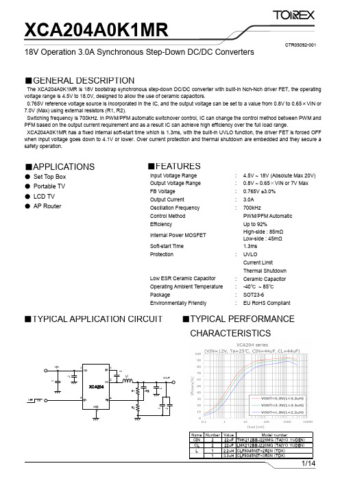
XCA204A0K1MR18V Operation 3.0A Synchronous Step-Down DC/DC Converters■FEATURESInput Voltage Range : 4.5V ~ 18V (Absolute Max 20V) Output Voltage Range : 0.8V ~ 0.65×VIN or 7V Max FB Voltage : 0.765V ±3.0% Output Current : 3.0A Oscillation Frequency : 700kHzControl Method PWM/PFM Automatic EfficiencyUp to 92%Internal Power MOSFET High-side : 85mΩ Low-side : 45mΩ Soft-start Time 1.3ms Protection : UVLO Current LimitThermal Shutdown Low ESR Ceramic Capacitor : Ceramic Capacitor Operating Ambient Temperature : -40℃ ~ 85℃ Package: SOT23-6Environmentally Friendly:EU RoHS Compliant■GENERAL DESCRIPTIONThe XCA204A0K1MR is 18V bootstrap synchronous step-down DC/DC converter with built-in Nch-Nch driver FET, the operatingvoltage range is 4.5V to 18.0V, designed to allow the use of ceramic capacitors. 0.765V reference voltage source is incorporated in the IC, and the output voltage can be set to a value from 0.8V to 0.65×VIN or 7.0V (Max) using external resistors (R1, R2). Switching frequency is 700kHz. In PWM/PFM automatic switchover control, IC can change the control method between PWM andPFM based on the output current requirement and as a result IC can achieve high efficiency over the full load range. XCA204A0K1MR has a fixed internal soft-start time which is 1.3ms, with the built-in UVLO function, the driver FET is forced OFF when input voltage goes down to 4.1V or lower. Over current protection and thermal shutdown are embedded and they secure a safety operation. ■APPLICATIONS ● Set Top Box● Portable TV● LCD TV ● AP Router ■TYPICAL APPLICATION CIRCUIT CTR05092-001■TYPICAL PERFORMANCE CHARACTERISTICSOF FON■BLOCK DIAGRAM■PRODUCT CLASSIFICATION●Ordering InformationProduct Name Package Name Order Unit Shipment XCA204A0K1MR SOT23-63,000pcs/ReelTape & Reel●Selection GuideChip EnableOver Voltage ProtectionThermal Shutdown Soft Start UVLO Current Limit YESYESYESYESYESYESGNDXCA204A0K1MRTOP VIEW■PIN CONFIGURATION■PIN ASSIGNMENTPIN NUMBER PIN NAME FUNCTION1 GND Ground. This pin is the voltage reference for the regulated output voltage. For this reason care must be taken in its layout.2 SW Switch Output. Connect this pin to the switching end of the inductor.3 VIN Power Supply Input. Drive 4.5V to 18V voltage to this pin to power on this chip. Connecting a 10μF~22μF ceramic bypass capacitor between VIN and GND to eliminate noise.4 FB Feedback. An external resistor divider from the output to GND, tapped to the FB pinsets the output voltage.5 EN ON/OFF Control Input. Pull EN above 1.8V to turn the device on.6 BS Bootstrap. A 100nF capacitor is connected between SW and BS pins to drive the power switch’s gate above the supply voltage.■FUNCTION CHARTPIN NAME SIGNAL STATUSEN L or OPEN Stand-byH ActiveGND SW VIN■ABSOLUTE MAXIMUM RATINGS(*1)Ta=25℃PARAMETER SYMBOL RATINGS UNITS Input Supply Voltage Pin V IN-0.3 ~ 20 V EN Voltage Pin V EN-0.3 ~ 20 VSW Voltage Pin V SW-0.3 ~ 20 VBoost Voltage Pin V BS V SW - 0.3 ~ V SW + 5.8 VFB Voltage Pin V FB-0.3 ~ 5.6 V Maximum Junction Temperature Tj 150 ℃Thermal resistance(Junction-Air) θJA88 ℃/W Thermal resistance(Junction-Case) θJC45 ℃/W Operating Ambient Temperature Topr -40 ~ 85 ℃Storage Temperature Tstg -65 ~ 150 ℃(*1) Stresses exceed those ratings may damage the device.XCA204A0K1MR ■ELECTRICAL CHARACTERISTICSTa=25℃PARAMETER SYMBOL CONDITIONS MIN. TYP. MAX. UNIT Input Voltage Range V IN 4.5 - 18.0 V Supply Current (Quiescent) I Q V EN = V IN, No switching - 300 - μA Supply Current (Shutdown) I STBY V EN = 0V - 3 10 μA Feedback Voltage V FB0.742 0.765 0.788 V Feedback Current I FB V FB = 1V -0.1 0 0.1 μA Switch-On High-Side Resistance (*1)R DSH(ON) - 85 - mΩSwitch-On Low-Side Resistance (*1)R DSL(ON)- 45 - mΩSwitch Leakage I SW V EN = 0V, V SW = 0V - - 10 μA Current Limit (*1)I OC DC current, V OUT =1.8V 3.1 4.0 - A Oscillator Frequency f SW V OUT = 5V@1A Load 560 700 880 kHz Soft-start time (*1)t SS V FB = 0V to 0.7V - 1.3 - ms Minimum ON-Time (*1)t ON- 150 - ns Minimum OFF-Time (*1)t OFF- 250 360 ns Under Voltage Lockout Threshold V UVLOR V IN Rising, V OUT = 1V - 4.1 4.4 VUnder Voltage LockoutV UVLOH V OUT = 1V - 250 - mV Threshold HysteresisEN pin resistance to GND R EN0.7 1.2 1.8 MΩEN Up Threshold Voltage V ENH 1.8 - 18.0 V EN Down Threshold Voltage V ENL GND - 0.4 V Thermal Shutdown (*1)T TSD- 150 - °C Test Condition: Unless otherwise stated, V IN=9V, V EN=2V(*1) Design reference value.■TYPICAL APPLICATION CIRCUITOF F ONFigure.1 Typical Application Circuit【Table1 : Recommended Component Selection】V OUT R1 R2 CFB L1 C1 C2 C3+C4(*)C5 C67.0V 81.5kΩ10kΩOptional 4.7μH 22μF/25VCeramic0.1μF/25VCeramic68μFCeramic0.1μFCeramic0.1μFCeramic5.0V 54.9kΩ10kΩOptional 3.3μH 22μF/25VCeramic0.1μF/25VCeramic44~68μFCeramic0.1μFCeramic0.1μFCeramic3.3V 33.2kΩ10kΩOptional 3.3μH 22μF/25VCeramic0.1μF/25VCeramic44~68μFCeramic0.1μFCeramic0.1μFCeramic1.8V 13.6kΩ10kΩOptional2.2μH 22μF/25VCeramic0.1μF/25VCeramic44~68μFCeramic0.1μFCeramic0.1μFCeramic1.0V 3.09kΩ10kΩOptional 1.5μH 22μF/25VCeramic0.1μF/25VCeramic44~68μFCeramic0.1μFCeramic0.1μFCeramic(*) V OUT=0.8V ~ 5.0V : (C3+C4) = 44μF to 68μF (Ceramic)V OUT=5.1V ~ 7.0V : (C3+C4) = 68μF (Ceramic)【Table2 : Parts example for evaluation】Name Number Value Parts number VenderL1 (*1) 1.5μH CLF6045NIT-1R5N TDK2.2μH CLF6045NIT-2R2N TDK3.3μH CLF6045NIT-3R3N TDK4.7μH CLF6045NIT-4R7N TDKC1 1 22μF TMK212BBJ226MG TAIYO YUDEN C2 1 0.1μF TMK105BJ104KP TAIYO YUDENC3, C4 (*2) 22μF LMK212BBJ226MG TAIYO YUDEN 68μF C3216X5R1A686M160AC TDKC5 1 0.1μF UMK105B7104KV TAIYO YUDEN C6 1 0.1μF UMK105B7104KV TAIYO YUDEN (*1) Select according to V OUT setting voltage.(*2) C3+C4=44μF : Two 22μF used in parallelXCA204A0K1MR■Function DescriptionThe main control loop of XCA204A0K1MR are adaptive on-time pulse width modulation (PWM) controller. The control mechanism combines adaptive on-time control with an internal compensation circuit for pseudo-fixed frequency and low external component count configuration with both low ESR and ceramic output capacitors. It is stable even with virtually no ripple at the output.At the beginning of each cycle, the high-side MOSFET is turned on. This MOSFET is turned off after internal one shot timer expires. This one shot duration is set proportional to the converter input voltage, VIN, and inversely proportional to the output voltage, V OUT, to maintain a pseudo-fixed frequency over the input voltage range, hence it is called adaptive on-time control. The one-shot timer is reset and the high-side MOSFET is turned on again when the feedback voltage falls below the reference voltage.< Enable >The XCA204A0K1MR EN pin provides digital control to turn on/turn off the regulator. When the voltage of EN exceeds the threshold voltage, the regulator starts the soft start function. If the EN pin voltage is below than the shutdown threshold voltage, the regulator will be disable and into the shutdown mode.< Output Over Voltage Protection >When the FB pin voltage exceeds 25% of the regulation voltage, the output over voltage protection function will turn the high side MOSFET off.< Input Under Voltage Lockout (UVLO) >When the XCA204A0K1MR power on, the internal circuits are held inactive until VIN exceeds the input UVLO threshold voltage. And the regulator will be disabled when VIN below the input UVLO threshold voltage. The hysteretic of the UVLO comparator is 250mV.< Short Protection >The XCA204A0K1MR provides short protection function to prevent the device damage from short condition. When the output short to ground, the oscillator frequency is reduced to prevent the inductor current increasing beyond the current limit. In the meantime, the current limit is also reduced to lower the short current. Once the short condition is removed, the frequency and current limit will return to normal.< Thermal Shutdown >The XCA204A0K1MR incorporates an over temperature protection circuit to protect itself from overheating. When the junction temperature exceeds the thermal shutdown threshold temperature, the regulator will be shutdown.■Application Information< Output Voltage Setting >The external resistor divider is used to set the output voltage. XCA204A0K1MR feedback resistors are unconcerned of compensation and provide an easy way to program output voltage. Table 1 shows a list of resistor selection for common output voltages:V OUT = 0.765V x (1+R1/R2)< Selecting the Inductor >A 4.7μH inductor with a DC current rating of at least 30% percent higher than the maximum load current is recommended for most applications. For highest efficiency, the inductor's DC resistance should be less than 50mΩ. For most designs, the required inductance value can be derived from the following equation:ΔΔΔΔ=0.3×ΔΔLL (MMMMMM )LL ≥VVVVVVVV ffffff ⋅ΔΔΔΔ⋅�1−VVVVVVVVVVΔΔVV�Where ΔI is the inductor ripple current.Choose the inductor ripple current to be 30% of the maximum load current. The maximum inductor peak current is calculated from:ΔΔLL (MMMMMM )=ΔΔLLLLMMLL (MMMMMM )+ΔΔΔΔ2But when a coil with poor DC superimposition(DC bias) characteristics is used, the inductor peak current may increase due to the derating of the inductor during soft start. In this case, please use a coil with better DC superimposition (DC bias) characteristics.Under light load conditions below 100mA, a larger inductance is recommended for improved efficiency.< Selecting the Input Capacitor >The input capacitor reduces the surge current drawn from the input supply and the switching noise from the device. The input capacitor impedance at the switching frequency should be less than the input source impedance to prevent high frequency switching current from passing through the input. Ceramic capacitors with X5R or X7R dielectrics are highly recommended because of their low ESR and small temperature coefficients. For most applications, a 22μF capacitor is sufficient.< Selecting the Output Capacitor >The output capacitor keeps the output voltage ripple small and one or two 22μF ceramic capacitor with X5R or X7R dielectrics is recommended for its low ESR characteristics.< External Boost Diode Selection >An external bootstrap diode is recommended if the input voltage is less than 5.5V, or duty cycle is high, or if there is a 5V system rail available. This diode helps improve the efficiency. Low cost diodes, such as B0520 are suitable for this application.V IN 5V C5D1B0520V IN 5VC5D1B0520V OUT 3.3V IND1B0520XCA204A0K1MR■Note on use1. When the VIN voltage is lower than UVLO and the temperature is low, there is a possibility of step-down operation.2. When the input voltage is low, the maximum load current may decrease.3. Be especially careful of the capacitor characteristics and use X7R or X5R (EIA standard) ceramic capacitors.The capacitance decrease caused by the bias voltage may become remarkable depending on the external size of the capacitor.4. Even within the operating temperature range, the thermal shutdown function may operate depending on the input voltage, output voltage and output current. An example of derating characteristics is shown below.Please evaluate IC well on your PCB.< PCB Layout Recommendation >The device’s performance and stability is dramatically affected by PCB layout. It is recommended to follow these general guidelines show bellow:1. Place the input capacitors, output capacitors as close to the device as possible. Trace to these capacitors should be asshort and wide as possible to minimize parasitic inductance and resistance.2. CIN must be closes to Pins VIN and GND. The loop area formed by CIN and VIN/GND pins must be minimized.3. The GND trace between the output capacitor and the GND pin should be as wide as possible to minimize its raceimpedance.4. Do not allow switching current to flow under the device.5. Place feedback resistors close to the FB pin. A separate V OUT path should be connected to the upper feedback resistor6. Keep the sensitive signal (FB) away from the switching signal (SW). The trace of the FB node should be as small aspossible to avoid noise coupling.7. Multi-layer PCB design is recommended.■TYPICAL PERFORMANCE CHARACTERISTICSC1=22μF, C2=0.1μF, C3=C4=22μF, C5=C6=0.1μF, Ta = 25℃, unless otherwise noted.Efficiency TestVin=12VSteady StateVin=12V,Vout=1.8V,Iout=0ASteady StateVin=12V,Vout=1.8V,Iout=2.0A Vo u t S W ILS W Vo u t ILDynamic loadingVin=12V,Vout=1.8V,Iout=0.3 to 2.7A, 0.5A/usIo u tPower OnVin=12V,Vout=1.8V,Iout=2.0AEN Vo u t ILShut DownVin=12V,Vout=1.8V,Iout=2A ENVo u tILVo ut■PACKAGING INFORMATION●SOT23-6 (unit:mm)(PCB FOOTPRINT)NOTES:1. JEDEC OUTLINE: N/A2. DIMENSIONS “D” DOES NOT INCLUDE MOLD FLASH, PROTRUSIONS OR GATE BURRS.MOLD FLASH,PROTRUSIONS AND GATE BURRS SHALL NOT EXCEED .15mm (.006in) PER SIDE.3. DIMENSIONS “E” DOES NOT INCLUDE INTER-LEAD FLASH, OR PROTRUSIONS. INTER-LEAD FLASH ANDPROTRUSIONS SHALL NOT EXCEED .25mm (.010in) PER SIDE.■MARKING RULE。
XD312-15-800V超宽电压输入DC-DC降压电源转换器模块手册
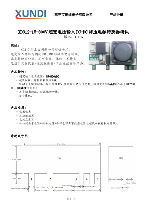
XD312-15-800V超宽电压输入DC-DC降压电源转换器模块版本:1.0.5概述:XD312为本公司新一代超低功耗、超宽输入电压范围的DC—DC非隔离电源模块,具有转换高效率、高可靠性、体积小等特点,适应于仪器仪表/电流互感器/工业遥控器等产品。
产品特性:•超宽输入电压范围:15-800VDC;•超低功耗:待机功耗低至5mW;• 3.6W最大输出功率:输出电压12V(其他输出电压可定制),输出电流300mA(输入小于400VDC 时),(恒流型可定制);•具有输出短路、过流保护功能;•超小体积。
产品应用:•仪器仪表•工业遥控器•电流互感器•低功耗要求电器的待机电源(如绿色环保节能型电器之超低功耗待机电源等)。
外观尺寸图:引脚编号名称功能描述1VIN-负电源输入脚2VIN+正电源输入脚3VOUT+正电源输出脚4CIN外接电容到3脚(VOUT+) 5VOUT-负电源输出脚说明:实际应用中超过上述极限值可能会导致电源模块的永久性损坏。
电气参数:注:1.在输入电压小于模块设定输出电压时,那么模块会以直通模式输出,输出100mA 时,压差0.8V左右;输出250mA时,压差2V左右。
2.上述参数值为常温环境测试下的典型值,实际应用中因工作环境不同可能有所差异。
3.如使用环境温度过高,输出电流需降额使用,具体以实际测试为准。
注:1.C1,C2容量串联后最少需大于2uF,耐压值串联后也应大于输入电压。
当输入处于交流宽范围供电(如AC18~AC400)时,C1,C2建议取10uF及以上。
2.C3取值:输入处于交流宽范围供电(如AC18~AC400)时,C3使用470uF;纯直流供电(如电瓶等)取100uF至220uF即可。
3.D1耐压需大于输入电压。
警告:因该模块为高压供电电源模块,其中将涉及到高电压,为了你的人身与设备安全,在上电调试过程中建议使用交流隔离电源来供电!。
dcdc 原理
dcdc 原理DC-DC转换器原理一、什么是DC-DC转换器?DC-DC转换器是一种电子元件,其作用是将直流电压(如12V)转换为另一种直流电压(如5V)。
它被广泛应用于各种电子设备中,例如手机、笔记本电脑、汽车电子设备等。
其中最常见的两种类型为降压型(Buck)和升压型(Boost),分别可以将输入电压降低或提高到所需的输出电压。
二、为什么需要DC-DC转换器?在许多电子设备中,需要使用不同的工作电压。
例如,在手机中,CPU需要3.3V的供应电压,但通信模块需要2.8V的供应电压。
如果使用一个固定的输入电源来提供所有这些不同的工作电压,那么这个输入电源必须能够提供最高工作电压,并且会浪费很多能量。
因此,使用一个可调节输出的 DC-DC转换器可以更有效地利用能量,并且使得整个系统更加灵活。
三、降压型(Buck) DC-DC转换器原理1. 基本原理降压型 DC-DC 转换器通过周期性切断输入直流源来实现输出电压的降低。
转换器包括一个开关管、一个输出电感和一个输出电容。
当开关管导通时,输入直流源的电能被存储在电感中。
当开关管关闭时,电感中的磁场会产生反向电势,将存储的能量传递给输出负载。
2. 工作原理在降压型 DC-DC 转换器中,开关管周期性地切换导通和断开状态。
当开关管导通时,输入直流源的正极连接到输出负载,并且输出电容开始充电。
在这个阶段,输入直流源通过开关管向输出负载提供能量。
当开关管关闭时,输入直流源断开与输出负载的连接,并且反向电势在输出端产生。
此时,输出电容将释放其存储的能量,并向负载提供所需的能量。
这个过程一直重复进行,在每个周期内,输出端都会得到一定数量的能量。
3. 具体实现降压型 DC-DC 转换器通常由以下几个部分组成:(1)PWM控制器:用于控制开关管的导通和断开状态。
(2)MOSFET(或IGBT):用于实现开关功能。
(3)输入滤波器:用于消除输入信号中的高频噪声。
(4)输出电感:用于存储和传递能量。
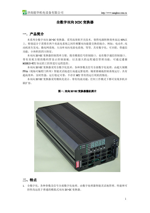
双向DCDC直流变换器,直流变换电源,直流升压降压转换器
1.3 – 4.0
< 1mS < 0.5S
5KW 6KW 0-25A(外输入电压控制) 1-10A(数码管设置) 200V–450V 可调,误差±2% 400V–800V 可调,误差±2% 2 A/V < 2% < 1V < 5%
6
济南能华机电设备有限公司
本双向 DC-DC 变换器采用模块化设计,带有均流功能,任何工作模式下都可实现多机并 联扩容。
图一.双向 DC-DC 变换器整机照片
二、特点
1. 全数字化,各种参数及信号全部数字化处理,由数字处理器智能灵活地管理。性能和可 控性均远优于普通的模拟式双向 DC-DC 变换器。
1
济南能华机电设备有限公司
PDn 为降压模式控制信号输入端,当 PDn 输入 3.3V ~5V 的高电平,并且 PUp 为低电平 时,双向逆变器为降压工作模式,电流从高压端子 IFHV 流入,经变换器变换为低压后,从 低压端子 IFLV 输出。
PUp 为升压模式控制信号输入端,当 PUp 输入 3.3V ~5V 的高电平,并且 PDn 为低电平 时,双向逆变器为升压工作模式,电流从低压端子 IFLV 流入,经变换器变换为高压后,从 高压端子 LFHV 输出。
> 95% < 12W < 20W 温控风冷 -25℃ - 60℃ 80℃
28A
15A
√ 5S
5S
315mm X140mm X 85mm 2.5Kg
八.产品图片
7
济南能华机电设备有限公司 图十.模块线路板照片(正面)
图十.模块线路板照片(反面)
图十一.模块接线图
在恒流模式时,Iout 总是正值(忽略电流源等效内阻消耗)。 图七. DC-DC 变换器恒流模式等效电路模型
- 1、下载文档前请自行甄别文档内容的完整性,平台不提供额外的编辑、内容补充、找答案等附加服务。
- 2、"仅部分预览"的文档,不可在线预览部分如存在完整性等问题,可反馈申请退款(可完整预览的文档不适用该条件!)。
- 3、如文档侵犯您的权益,请联系客服反馈,我们会尽快为您处理(人工客服工作时间:9:00-18:30)。
TPS5405 是一款具有宽运行输入电压范围(6.5 V 至 28 V) 的单片非同步降压稳压器。
此器件执行内部斜坡补偿的电流模式控制来减少组件数量。
TPS5405 还特有一个轻负载脉冲跳跃模式,此特性可在轻负载时减少为系统供电的输入电源的功率损失。
∙故定 5-V 输出∙ 6.5-V 至 28-V 的宽输入电压范围∙高达 2-A 的最大持续输出负载电流器件用途∙9-V,12-V 和 24-V 分布式电源系统∙消费类应用,诸如家用电器、机顶盒、CPE 设备、LCD 显示器、外设、和电池充电器∙工业用和车载娱乐系统电源TPS54495 是一款双路、自适应接通时间D-CAP2™ 模式同步降压转换器。
TPS54495 可帮助系统设计人员通过成本有效性、低组件数量、和低待机电流解决方案来完成各种终端设备的电源总线调节器集。
TPS54495 的主控制环路采用D-CAP2™ 模式控制,无需外部补偿组件即可提供极快的瞬态响应。
自适应接通时间控制支持更高负载状态下的脉宽调制(PWM) 模式与轻负载下的Eco-mode™ 工作模式之间的无缝转换。
Eco-mode™ 使TPS54495 能够在较轻负载条件下保持高效率。
TPS54495 也能够去适应诸如高分子有机半导体固体电容器(POSCAP) 或者高分子聚合物电容器(SP-CAP) 的低等效串联电阻(ESR) ,和超低ESR,陶瓷电容器。
此器件在输入电流为4.5V 至18V 之间时提供便捷和有效的运行。
特性∙D-CAP2 控制模式o快速瞬态响应o环路补偿无需外部部件o与陶瓷输出电容器兼容∙宽输入电压范围:4.5V 至 18V∙输出电压范围:0.76V 至 7.0V∙针对低占空比应用对高效集成 FET 进行了优化o90mΩ(高侧)和 60mΩ(低侧)∙高初始基准精度∙支持恒定 4A 通道 1 和 2A 通道 2 负载电流∙低侧 r DS(接通)低损失电流感测∙可调软启动∙非吸入预偏置软启动∙700kHz 开关频率∙逐周期过流限制控制∙过流限制 (OCL) / 欠压闭锁 (UVLO) / 热关断 (TSD) 应用∙用于过载保护的断续定时器∙带有集成式升压 P 通道场效应晶体管 (PMOS) 开关的自适应栅极驱动器∙由于热补偿 r DS(接通)的值为4000ppm/℃ ,过流保护 (OCP) 恒定∙16 引脚散热薄型小外形尺寸封装 (HTSSOP)∙自动跳跃 Eco-mode 为了在轻负载下实现高效率TPS53318 和 TPS53319 是带有集成型 MOSFET 的 D-CAP™ 模式,8A 或者 14A 同步转换器。
它们被设计用于易于使用、低外部组件数量、和空间有限的电源系统。
这些器件特有精准的 1%,0.6V 基准,和集成的升压开关。
具有竞争力的特性包括:1.5V 至 22V 的宽转换输入电压范围、极低的外部组件数量、用于超快速响应的 D-CAP™ 模式控制、自动跳跃模式操作、内部软启动控制、可选频率、且无需补偿。
转换输入电压介于 1.5V 至 22V 之间,电源电压从 4.5V 至 25V,输入电压范围为 0.6V 至 5.5V。
这些器件采用 5mmx6mm,22 引脚 QFN 封装,额定工作温度范围为 -40°C 至85°C。
特性∙转换输入电压范围:1.5V 至 22V∙漏极电源电压 (VDD) 输入电压范围:4.5V 至 25V∙14A 时,在 12V 至 15V 之间效率达到 91%∙输出电压范围:0.6V 至 5.5V∙5V 低压降 (LDO) 输出∙支持单电源轨出入∙带有 8A (TPS53318) 或者 14A (TPS53319) 持续输出电流的集成型功率金属氧化物半导体场效应晶体管 (MOSFET)∙用于轻负载有效性的自动跳跃 Eco-mode™∙<100μA 的关断电流∙具有快速瞬态响应的 D-CAP™ 模式∙可借助外部电阻器在 250kHz 至 1MHz 之间选择开关频率∙可选的自动跳跃或者只支持脉宽调制 (PWM) 运行∙内置 0.6V 基准电压 (1%)。
∙0.7ms,1.4ms,2.8ms 和 5.6ms 可选内部电压伺服系统软启动∙集成升压开关∙预充电启动功能∙带有热补偿的可调过流限制∙过压、欠压、欠压闭锁 (UVLO) 和过热保护∙支持所有陶瓷输出电容器∙开漏电源良好指示∙组装有 NexFET 电源块技术∙22 引脚,四方扁平无引线 (QFN) 封装并带有 PowerPADTPS54526 是一款自适应接通时间D-CAP2™ 模式同步降压转换器。
TPS54526 可帮助系统设计人员通过低成本、低组件数量的低待机电流解决方案来完成各种终端设备的电源总线调节器集。
TPS54526 的主控制环路采用D-CAP2™ 模式控制,无需外部补偿组件便可实现极快的瞬态响应。
自适应接通时间控制可在更高负载状态下的脉宽调制(PWM) 模式与轻负载下的Eco-mode™ 工作之间实现无缝转换。
Eco-mode™ 使TPS54526 能够在较轻负载状况下保持高效率。
TPS54526 的专有电路还可使该器件能够适应POSCAP 与SP-CAP 等低等效串联电阻(ESR) 输出电容器以及超低ESR 陶瓷电容器。
该器件的工作输入电压介于4.8V 至18V 之间。
可在0.76V 至5.5V 的范围内对输出电压进行编程。
此外,该器件还支持可调软启动时间与功率良好功能。
TPS54526 采用14 引脚散热薄型小外形尺寸(HTSSOP) 封装与16 引脚四方扁平无引线(QFN) 封装,设计运行温度范围从-40°C 到85°C。
TPS53318 和 TPS53319 是带有集成型 MOSFET 的 D-CAP™ 模式,8A 或者 14A 同步转换器。
它们被设计用于易于使用、低外部组件数量、和空间有限的电源系统。
这些器件特有精准的 1%,0.6V 基准,和集成的升压开关。
具有竞争力的特性包括:1.5V 至 22V 的宽转换输入电压范围、极低的外部组件数量、用于超快速响应的 D-CAP™ 模式控制、自动跳跃模式操作、内部软启动控制、可选频率、且无需补偿。
转换输入电压介于 1.5V 至 22V 之间,电源电压从 4.5V 至 25V,输入电压范围为 0.6V 至 5.5V。
这些器件采用 5mmx6mm,22 引脚 QFN 封装,额定工作温度范围为 -40°C 至85°特性∙转换输入电压范围:1.5V 至 22V∙漏极电源电压 (VDD) 输入电压范围:4.5V 至 25V∙14A 时,在 12V 至 15V 之间效率达到 91%∙输出电压范围:0.6V 至 5.5V∙5V 低压降 (LDO) 输出∙支持单电源轨出入∙带有 8A (TPS53318) 或者 14A (TPS53319) 持续输出电流的集成型功率金属氧化物半导体场效应晶体管 (MOSFET)∙用于轻负载有效性的自动跳跃 Eco-mode™∙<100μA 的关断电流∙具有快速瞬态响应的 D-CAP™ 模式∙可借助外部电阻器在 250kHz 至 1MHz 之间选择开关频率∙可选的自动跳跃或者只支持脉宽调制 (PWM) 运行∙内置 0.6V 基准电压 (1%)。
∙0.7ms,1.4ms,2.8ms 和 5.6ms 可选内部电压伺服系统软启动∙集成升压开关∙预充电启动功能∙带有热补偿的可调过流限制∙过压、欠压、欠压闭锁 (UVLO) 和过热保护∙支持所有陶瓷输出电容器∙开漏电源良好指示∙组装有 NexFET 电源块技术∙22 引脚,四方扁平无引线 (QFN) 封装并带有 PowerPADTPS54061 是一款 60V,200 mA,同步降压直流到直流转换器,此转换器具有集成的高侧和低侧 MOSFET。
电流模式控制提供了简单的外部补偿和灵活的组件选择。
非开关电源电流为90µA。
使用使能引脚可将关断电源电流减少至 1.4µA。
为了增加轻负载时的效率,当电感器电流达到零时,低侧 MOSFET 仿真一个二极管。
欠压闭锁内部设定为 4.5V,但可采用两个使能引脚上的电阻器将其提高。
输出电压启动斜坡由内部慢启动时间控制。
可调节开关频率范围可实现高效率和外部组件尺寸优化。
频率折返和热关断功能负责在过载情况下对器件提供保护作用。
TPS54061 通过集成 MOSFET,引导再充电二极管,以及大大减小封装尺寸(使用小型 3mm x 3mm 散热增强型 VSON 封装)来实现小型设计。
TPS54061 的技术支持由 Webench 设计人员提供在上提供。
特性∙集成的高侧和低侧场效应晶体管 (MOSFET)∙用于提升轻负载效率的二极管仿真∙峰值电流模式控制∙90µA 运行静态电流∙ 1.4µA 关断电源电流∙50kHz 至 1100kHz 可调开关频率∙同步至外部时钟∙内部慢启动∙0.8V±1% 电压基准∙与陶瓷输出电容器或者低成本铝制电解电容器一起工作时保持稳定∙逐周期电流上限、过热、过压保护 (OVP) 和频率折返保护∙带有散热垫的 3mm x 3mm 超小型小外形尺寸无引线 (VSON)-8 封装∙-40°C 至150°C 运行结温TPS54160A 器件是一款带有集成型高侧 MOSFET 的 60V,1.5A,降压稳压器。
电流模式控制提供了简单的外部补偿和灵活的组件选择。
一个低纹波脉冲跳跃模式将无负载的稳定输出电源电流减小至 116μA。
采用使能引脚可将停机模式的电源电流降低至 1.3μA。
欠压闭锁在内部设定为 2.5V,但可采用使能引脚将之提高。
输出电压启动斜坡受控于缓慢起动引脚,该引脚还可以通过配置来控制排序/跟踪。
一个开漏电源良好信号表示输出处于其标称电压的 93% 至 107% 之内。
宽开关频率范围允许对效率及外部组件尺寸进行优化。
频率折返和热关断功能在过载情况下对部件实施保护。
特性∙ 3.5V 至 60V 输入电压范围∙200mΩ高侧金属氧化物半导体场效应晶体 (MOSFET)∙在带有脉冲跳跃的轻负载条件上实现了高效率 Eco-mode∙为了实现更加精准的欠压锁定 (UVLO) 电压,此器件的使能阀值比TPS54160 更严密∙可调的 UVLO 电压和滞后∙116μA 工作静态电流∙ 1.3μA 关断电流∙100kHz 至 2.5MHz 的开关频率∙同步至外部时钟∙可调节的缓慢起动/排序∙欠压 (UV) 和过流 (OV) 电源良好输出∙0.8V 内部电压基准∙具有 PowerPAD∙由 WEBBENCH 支持和 SwitcherPro 软件工具提供∙For SWIFT 如需查阅文档,请登录 TI 网站/swiftTPS54140A 器件是一款 42V,1.5A,降压稳压器,此稳压器具有一个集成的高侧MOSFET。