MP1584EN3A,15MHz的,28V降压型转换器中文
士兰微 400KHz 2A降压型DC-DC转换器 说明书

电感选择
当输出电流较大时,转换器工作在连续电流模式,即电 感电流连续,不会降至 0。电感的取值会影响到电感电流的纹 波,两者之间的关系由下式确定。
L = VO ⋅(VI − VO ) 。 VI ⋅ fS ⋅ ΔI
其中,VI 是输入电压, VO 是输出电压, fS 是开关频率, ΔI 是电感电流纹波的峰-峰值。通
⋅ fZ1
。
当需要补偿电容 Cc2 时,Cc2 的值由下式确定:
CC2
=
ESR ⋅ CO RC
。
典型应用电路图
杭州士兰微电子股份有限公司 http:
版本号:1.0 2008.09.26 共8页 第7页
封装外形图
SOP-8-225-1.27
SD46520
UNIT: mm
常选择 ΔI 不超过最大输出电流的 30%,以此来确定电感的取值。
同时,还必须满足电感电流的峰值不能超过 2.4A 电流限制值的条件。电感电流的峰值由下式 确定。
ILMAX
= IO
+
1 2
⋅
ΔIL
= IO
+
1 2
⋅
VO ⋅(VI − VO ) VI ⋅ fS ⋅L
。
输入电容选择
降压性DC-DC的输入电流是不连续的,需要在输入端添加输入电容CI保持输入电压的稳定。 输入电容必须是低ESR的电容类型。最好是陶瓷电容,钽电容或低ESR的电解电容也可以。输入 电容值必须大于 10uF。
版本号:1.0 2008.09.26 共8页 第1页
内部框图
SD46520
极限参数
参数 输入电压 开关电压 自举电压 反馈电压 使能端电压 补偿端电压 结温 引脚温度 存储温度
TD1501 3A 150KHZ 45V PWM Buck DC DC 转换器数据表说明书

General DescriptionThe TD1501 is a of easy to use adjustable step-down (buck) switch-mode DC/DC converter. The device is available in an adjustable or fixed output version. It is capable of driving a 3A load with excellent line and load regulation.The output voltage is guaranteed to ±3% tolerance under specified input voltage and output load conditions. The oscillator frequency is guaranteed to ±15%.The PWM control circuit is able to adjust the duty ratio linearly from 0 to 100%. External shutdown is included, featuring typically 80 µA standby current. Self protection features include a two stage frequency reducing current limit for the output switch and an over temperature shutdown for complete protection under fault conditions. Requiring a minimum number of external components, these regulators are simple to use and include internal frequency compensation, and a fixed-frequency oscillator.The TD1501 is available in TO-220B-5L and TO-263-5L packages. Features• Voltage mode non-synchronous PWM control • Built- in switching transistor on chip• Guaranteed 3A output load current• Input voltage range up to 45V• 3,3V,5V and Adjustable output versions• adjustable version output from 1.23V to 42V • Fixed 150KHz frequency internal oscillator• Up to 90% efficiency• ON/OFF shutdown control input• Low power standby mode, I Q typically 80 µA • Thermal shutdown , current limit and short circuit protection• Available in TO-220B and TO-263 packages • RoHS Compliant (100% Green available) • The minimum dropout @ Vout=5V/0.5A up to 0.9 VApplications• Simple High-efficiency step-down regulator• On-card switching regulators• Positive to negative converter• LCD monitor and LCD TV• DVD recorder and PDP TV• Battery charger• Step-down to 1.8/2.5/3.3/5.0 V formicroprocessorsPackage TypesTO220-5LJune, 01, 2013 Rev 2.3 Techcode Semiconductor LimitedPin AssignmentsPin DescriptionsOrdering InformationName DescriptionVin Input supply voltageOutput SwitchingoutputGnd GroundFeedbackOutput voltage feedbackinputON/OFFON/OFF shutdownActive is “Low” or Ground 5 ON/OFF4 Feedback3 Gnd2 Output1 VinGNDTAB ISGNDTO220-5LTO263-5LFunction DescriptionPin Functions+V INThis is the positive input supply for the IC switching regulator. A suitable input bypass capacitor must be present at this pin to minimize voltage transients and to supply the switching currents needed by the regulator.GNDCircuit ground.OutputInternal switch. The voltage at this pin switches between (+V IN – V SAT) and approximately – 0.5V, with a duty cycle of approximately V OUT / V IN. To minimize coupling to sensitive circuitry, the PC board copper area connected to this pin should be kept a minimum.FeedbackSenses the regulated output voltage to complete the feedback loop.ON/OFFAllows the switching regulator circuit to be shutdown using logic level signals thus dropping the total input supply current to approximately 80uA. Pulling this pin below a threshold voltage of approximately 1.3V turns the regulator on, and pulling this pin above 1.3V (up to a maximum of 32V) shuts the regulator down. If this shutdown feature is not needed, the ON /OFF pin can be wired to the ground pin , the regulator will be in the ON condition. The ON /OFF pin should not be left open .Functional Block DiagramFigure 2. Functional Block Diagram of TD1501Typical ApplicationFigure 3. Typical Application of TD1501Absolute Maximum RatingsUnitValueParameter SymbolInput Voltage V IN-0.3 to 45 VFeedback Pin Voltage V FB-0.3 to 40 VEnable Pin Voltage Von-off -0.3 to 40 VOutput Voltage to Ground (Steady State)e V OUT-1 V Power Dissipation P D Internally limited mWOperating Junction Temperature T J150 ºC Storage Temperature T STG-65 to 150 ºCLead Temperature (Soldering, 10 sec) T LEAD260 ºCESD (HBM) V ESD2000 VNote1: Stresses greater than those listed under Maximum Ratings may cause permanent damage tothe device. This is a stress rating only and functional operation of the device at these or any other conditions above those indicated in the operation is not implied. Exposure to absolute maximumrating conditions for extended periods may affect reliability.Recommended Operating ConditionsUnitMax.Parameter SymbolMin.Input Voltage V IN 3.6 45 V Operating Junction Temperature T J -40 125 ºC Operating Ambient Temperature T A -40 85 ºCElectrical Characteristics (All Output Voltage Versions)Unless otherwise specified, VIN = 12V for 3.3V, 5V, adjustable version . I LOAD = 0.5A Ta = 25ºC.Symbol ParameterConditionsMin. Typ. Max. UnitV IN Input voltage 4.5 45 VI Q Quiescent current V FB =12V force driver off34mAOutput=0VNo outside circuitV FB =12V force driver off50 uAI LOutput=-1VOutputleakage currentV IN =40V 2 30 mAI STBYStandby quiescentcurrentON/OFF pin=5V, V IN =32V80 200uAFosc Oscillator Frequency 125 150 170 KHz FSCPOscillator Frequency of Short Circuit ProtectWhen current limit occurred and VFB < 0.5V, Ta = 25℃ 10 30 50 KHz V SAT Saturation voltageI OUT =3ANo outside circuitV FB = 0V force driver on 1.16 1.4 V Max. Duty Cycle (ON)V FB = 0V force driver on 100 DCMin. Duty Cycle (OFF) V FB =12V force driver off% V FBFeedback Voltage V IN = 4.5V to 45 V1.21 1.235 1.26VI FB Feedback bias current V FB =1.3V(Adjustable version only)10 50 nAI CL Current LimitPeak Current (V FB =0V) 3.8 5.5 A V IL Low (Regulator ON) 1.30.6V V IH ON/OFF pin logic inputThreshold voltage High (Regulator OFF)2.01.3VI H ON/OFF pin logic input currentV LOGIC =2.5V(OFF)-0.01 uA I L ON/OFF pin input currentV LOGIC =0.5V(ON) -0.1 uA θJC Thermal ResistanceTO220B-5LTO263-5L Junction toCase2.53.5OC/W θJA Thermal Resistance with a copper area of approximately 3 in 2TO220B-5L TO263-5LJunction to Ambient2823OC/WElectrical Characteristics ( Continued )Specifications with boldface type are for full operationg temperature range, the other type are for T J=25O C.Typical Performance CharacteristicsFigure 4. Efficiency vs. Load (Vin=12V)Figure 5. Output Voltage vs. TemperatureFigure 6. Output Saturation Characteristics Figure 7. Switching Frequency vs. TemperatureFigure 9. ON/OFF Pin Voltage Figure 10. ON/OFF Pin Sink CurrentFigure 8. Quiescent Current vs. TemperatureFigure 11. Output Saturation CharacteristicsTypical Application Circuit (3.3V Fixed Output Voltage Version)Output ComponentInput Voltage Inductor(L1)Through HoleElectrolytic(Cout)Surface MountTantalum(Cout)Schottky Diode(D1)4.5V ~ 18V 47uh 470uf/25V 330uf/6.3V 18V ~ 45V 68uh 560uf/25V 330uf/6.3V ref. Table 5Figure 11. Typical Application of TD1501 For 3.3VTable 1. TD1501 Series Buck Regulator Design Procedure For 3.3VTypical Application Circuit (5V Fixed Output Voltage Version)Output ComponentInput Voltage Inductor(L1)Through HoleElectrolytic(Cout)Surface MountTantalum(Cout)Schottky Diode(D1)7V ~ 18V 33uh 330uf/25V 220uf/10V 18V ~ 45V 47uh 470uf/25V 330uf/10V ref. Table 5Figure 12. Typical Application of TD1501 For 5VTable 2. TD1501 Series Buck Regulator Design Procedure For 5VTypical Application Circuit (Adjustable Output Voltage Version)Vout R1 R2 Cf (Optional)3.3V 1.6K 2.7K33nf 5V 3.6K 11K 10nf 9V 6.8K43K 1.5nf 12V 1.5K 13K1nfOutput ComponentOutputVoltage Input Voltage Inductor (L1)Through Hole Electrolytic (Cout) Schottky Diode( D1 )4.5V ~ 18V 47uh 470uf/25V 3.3V 18V ~45V 68uh 560uf/25V 7V ~ 18V 33uh 330uf/25V 5V 18V ~45V 47uh 470uf/25V 12V ~18V 47uh 330uf/25V 9V 18V ~45V 47uh 470uf/25V 15V ~ 18V 47uh 220uf/25V 12V18V ~45V47uh330uf/25Vref. Table 5Figure 13. Typical Application of TD1501 For ADJ Table 3. Vout VS. R1, R2, Cf Select Table Table 4. Typical Application Buck Regulator Design ProcedureSchottky Rectifier Selection GuideVin2A Load Current 3A Load Current(Max) Part Number Package Vendor Part Number Package Vendor B220/A SMB/SMA 1 B320/B/ASMC/B/A 1 SS22 SMA 2,3 SS32 SMC 2,320 V- - - MBRS320 SMC 4- - - SK32 SMC 6- - - IN5820 D0-201AD 6 B230/A SMB 1 B330/B/ASMC/B/A 1 SS23 SMB 2,3 SS33 SMC 2,330 V20BQ030 SMB 4 MBRS330SMC 4,5 MBRS230 SMB 5 SK33 SMC 3,6SK23 SMB 6 IN5821 D0-201AD 2,6B240/A SMB/SMA 1 B340/B/ASMC/B/A 1 SS24 SMB 2,3,5 SS34 SMC 2,3MBRS240 SMB 5 30BQ040SMC 440 V- - - MBRS340TRSMC 4,5- - - SK34 SMC 6- - - IN5822 DC-201AD 6 B250/A SMB/SMA 1 B350/B/ASMC/B/A 1 SS25 SMB 2,3 SS35 SMC 2,350 VSK23 SMB 6 MBRS330SMC 4,5- - - SK35 SMC 3,64A Load Current 5A Load CurrentVin(Max) Part Number Package Vendor Part Number Package Vendor SL42 SMC 2,3 B520C SMC 1- - - SR502 D0-201AD 120 V- - - SB520 D0-201AD 2- - - IN5823 D0-201AD 6 SL43 SMC 2,3 B530C SMC 1- - - SR503 D0-201AD 130 V- - - SB530 D0-201AD 2,- - - SSC53L SMC 3- - - IN5824 D0-201AD 6 SL44 SMC 2,3,5 B540C SMC 1- - - SR504 D0-201AD 1- - - SB540 DC-201AD 240 V- - - SSC54 SMC 3- - - MBRS540T3 SMC 5- - - IN5825 DC-201AD 6- - - B550C SMC 150 V- - - SB550 DC-201AD 2- - - - - -Table 5 Lists some rectifier manufacturers.No. Vendor WebSiteInc. 1 Diodes,2 FairchildSemiconductor Semiconductor 3 GeneralRectifier 4 International5 OnSemiconductor 6 Pan Jit International Table 6 Schottky Diode manufacturers.Application Hints and Layout GuidelinesHeat Sink / Thermal ConsiderationsThe TD1501 is available in two packages, a 5-pin TO-220B/TO220 and a 5-pin surface mount TO-263. The TO-220B/TO220 package needs a heat sink under most conditions. The size of the heatsink depends on the input voltage, the output voltage, the load current and the ambient temperature. The TD1501 junction temperature rises above ambient temperature for a 3A load and different input and output voltages. The data for these curves was taken with the TD1501 (TO-220B/TO220 package) operating as a buck switching regulator in an ambient temperature of 25o C (still air). These temperature rise numbers are all approximate and there are many factors that can affect these temperatures. Higher ambient temperatures require more heat sinking.The TO-263 surface mount package tab is designed to be soldered to the copper on a printed circuit board. The copper and the board are the heat sink for this package and the other heat producing components, such as the catch diode and inductor. The PC board copper area that the package is soldered to should be at least 0.4 in2, and ideally should have 2 or more square inches of 2 oz. Additional copper area improves the thermal characteristics, but with copper areas greater than approximately 6 in2, only small improvements in heat dissipation are realized. If further thermal improvements are needed, double sided, multilayer PC board with large copper areas and/or airflow are recommended.The TD1501 (TO-263 package) junction temperature rise above ambient temperature with a 3A load for various input and output voltages. This data was taken with the circuit operating as a buck switching regulator with all components mounted on a PC board to simulate the junction temperature under actual operating conditions. This curve can be used for a quick check for the approximate junction temperature for various conditions, but be aware that there are many factors that can affect the junction temperature. When load currents higher than 3A are used, double sided or multilayer PC boards with large copper areas and/or airflow might be needed, especially for high ambient temperatures and high output voltages.For the best thermal performance, wide copper traces and generous amounts of printed circuit board copper should be used in the board layout. (Once exception to this is the output (switch) pin, which should not have large areas of copper.) Large areas of copper provide the best transfer of heat (lower thermal resistance) to the surrounding air, and moving air lowers the thermal resistance even further. Output Voltage Ripple and TransientsThe output voltage of a switching power supply will contain a sawtooth ripple voltage at the switcher frequency, typically about 1% of the output voltage, and may also contain short voltage spikes at the peaks of the sawtooth waveform.The output ripple voltage is due mainly to the inductor sawtooth ripple current multiplied by the ESR of the output capacitor.The voltage spikes are present because of the fast switching action of the output switch, and the parasitic inductance of the output filter capacitor, To minimize these voltage spikes, special low inductance capacitors can be used, and their lead lengths must be kept short. Wiring inductance, stray capacitance, as well as the scope probe used to evaluate these transients, all contribute to the amplitude of these spikes.A large value inductor will also result in lower output ripple voltage , but will have a larger physical size,higher series reistance,and/or lower saturation current. An additional small LC filter can be added to the output (as shown in Figure 14) to further reduce the amount of output ripple and transients.Layout GuidelinesAs in any switching regulator, layout is very important. Rapidly switching currents associated with wiring inductance can generate voltage transients which can cause problems. For minimal inductance and ground loops, the wires indicated by heavy lines should be wide printed circuit traces and should be kept as short as possible. For best results, external components should be located as close to the switcher IC as possible using ground plane construction or single point grounding.If open core inductors are used, special care must be taken as to the location and positioning of this type of inductor. Allowing the inductor flux to intersect sensitive feedback, IC groundpath and C OUT wiring can cause problems.When using the adjustable version, special care must be taken as to the location of the feedback resistors and the associated wiring. Physically locate both resistors near the IC, and route the wiring away form the inductor especially an open core type of inductor.Figure 14, Layout Guidelines and Post Ripple FilterTDxxxxxTDxxxxxPackage Information (TO220B-5L)Dimensions In Millimeters Dimensions In Inches SymbolMin. Max. Min. Max.A 0.44 0.47 0.175 0.185b 0.07 0.09 0.027 0.037D 0.84 0.89 0.330 0.350d1 0.10 0.039d2 0.63 0.248E 9.91 10.41 0.390 0.410e 0.16 0.18 0.062 0.072F 0.12 0.13 0.048 0.052H1 0.64 0.250H2 2.08 2.24 0.820 0.880H3 2.39 2.55 0.942 1.002J1 0.27 0.105J2 0.37 0.53 0.147 0.207J3 0.84 0.331Q 0.25 0.30 0.100 0.120Package Information (TO220-5L)Package Information (TO263-5L)Dimensions In Millimeters Dimensions In Inches SymbolMin. Max. Min. Max.A 4.45 4.7 0.175 0.185B 0.71 0.97 0.028 0.038C 0.38 0.76 0.015 0.030C2 1.22 1.32 0.048 0.052D 8.38 8.89 0.330 0.350E 9.91 10.16 0.390 0.410e 1.57 1.85 0.062 0.070F 6.61 7.11 0.260 0.280L - 14.35 - 0.565L2 - 1.27 - 0.050Packing InformationTO263-5L Carrier Tape Outline DimensionsCarrier Tape, Number of Components Per Reel and Reel SizePackage Carrier Width (W) Pitch (P) Part Per Full Reel Reel Size TO263-5L 24.0 ± 0.1mm 4.0 ± 0.1mm 800 PCS 330 ± 2mm。
315VNSN820M35E中文资料(Nippon Chemi-Con)中文数据手册「EasyDatasheet - 矽搜」

(at 120Hz) The following specifications shall be satisfied when the capacitors are restored to 20C after subjected to DC voltage with the rated ripple current is applied for 3000 hours (2000 hours for F20mm products) at 105C. Capacitance change [P20% of the initial value DF (tanE) [200% of the initial specified value [The initial specified value Leakage current The following specifications shall be satisfied when the capacitors are restored to 20C after exposing them for 1000 hours at 105C without voltage applied. Capacitance change [P15% of the initial value [150% of the initial specified value DF (tanE) Leakage current [The initial specified value
22B25 1.00 22B25 1.20 22B30 1.35 22B35 1.50 22B40 1.67 22B45 1.78 22B50 2.04
30B20 1.15 30B20 1.20 30B25 1.50 30B25 1.67 30B30 1.78 30B30 2.04 30B35 2.30 30B40 2.55 30B45 2.90 30B60 3.49
凌特降压型DC-DC转换器

凌特降压型DC/DC转换器
2006 年8 月15 日-北京-凌特公司(Linear Technology Corporation)推出高效率、2.25MHz、同步降压型稳压器LTC3549,该器件能用低至1.6V 的输入电压提供高达250mA 的连续输出电流。
LTC3549 采用恒定频率和电流模式架构,用 1.6V 至 5.5V 的输入电压工作,非常适用于单节锂离子或两节碱性/镍镉/镍氢电池应用。
该器件可以产生低至0.61V 的输出电压,因此能够为最新一代低压DSP 和微控制器供电。
其2.25MHz 开关频率允许利用高度低于1mm 的纤巧和低成本陶瓷电容器和电感器,因而可为手持式应用组成占板面积非常紧凑的解决方案。
LTC3549 采用RDS(ON) 仅为0.4Ω(N 沟道)和0.56Ω(P 沟道)的内部开关,具有高达93% 的效率。
它还采用低压差100% 占空比工作模式,允许输出电压等于VIN,从而进一步延长了电池工作时间。
LTC3549 利用低纹波突发模式(Burst Mode®)工作,以低于20mVPK-PK 的输出纹波提供仅为50uA 的无负载静态电流。
如果应用是噪声敏感的,那么LTC3549 还可以设置为噪声更低的脉冲跳跃模式,而且仍然提供仅为300uA 的静态电流。
两种器件都保持停机电流低于1uA,从而进一步延长了电池寿命。
LTC3549 用陶瓷电容器可稳定,因而实现了非常低的输出电压纹波。
其它特点包括实现卓越电压和负载瞬态响应的电流模式工作、内部软启动以及过热保护。
MP1584

MP15843A, 1.5MHz, 28V Step-Down ConverterMPS CONFIDENTIAL AND PROPRIETARY INFORMATION – INTERNAL USE ONLYThe Future of Analog IC Technology DESCRIPTIONThe MP1584 is a high frequency step-downFEATURES• Wide 4.5V to 28V Operating Input Range OUTPUT CURRENT (A)ORDERING INFORMATIONPart Number* Package Top Marking Temperature MP1584EN SOIC8E MP1584EN –20°C to +85°CELECTRICAL CHARACTERISTICSV IN = 12V, V EN = 2.5V, V COMP = 1.4V, T A= +25°C, unless otherwise noted.PIN FUNCTIONSTYPICAL PERFORMANCE CHARACTERISTICSV IN = 12V, V OUT=5V, C1 = 10µF, C2 = 22µF, L1= 10µH, T A = +25°C, unless otherwise noted.1v.OUT SW OUT SW2v.2v.Oscillating Frequency vs R freqTYPICAL PERFORMANCE CHARACTERISTICS (continued)V IN = 12V, C1 = 10µF, C2 = 22µF, L1 = 10µH, f SW =500KHz, and T A = +25°C, unless otherwise noted.5ms/div.Startup1ms/div.Shutdown5ms/div.Startup5ms/div.BLOCK DIAGRAMError AmplifierThe error amplifier compares the FB pin voltage with the internal reference (REF) and outputs a current proportional to the difference between the two. This output current is then used to Internal Soft-StartThe soft-start is implemented to prevent the converter output voltage from overshooting during startup. When the chip starts, the internal circuitry generates a soft-start voltageAt higher duty cycle operation condition, the time period available to the bootstrap charging is less so the bootstrap capacitor may not be sufficiently charged.In case the internal circuit does not haveStartup and ShutdownIf both VIN and EN are higher than their appropriate thresholds, the chip starts. The reference block starts first, generating stable reference voltage and currents, and then theAPPLICATION INFORMATIONCOMPONENT SELECTIONSetting the Output VoltageThe output voltage is set using a resistiveA good rule for determining the inductance to use is to allow the peak-to-peak ripple current in the inductor to be approximately 30% of theTable 1—Inductor Selection GuideThe input capacitor (C1) can be electrolytic, tantalum or ceramic. When using electrolytic or tantalum capacitors, a small, high quality ceramic capacitor, i.e. 0.1μF, should be placed as close to the IC as possible. When usingMP1584 can be optimized for a wide range of capacitance and ESR values.Compensation ComponentsMP1584 employs current mode control for easy compensation and fast transient response. The system stability and transient response are controlled through the COMP pin. COMP pin isIn this case (as shown in Figure 2), a third pole set by the compensation capacitor (C6) and the compensation resistor (R3) is used to compensate the effect of the ESR zero on the loop gain. This pole is located at:1. Choose the compensation resistor (R3) to set the desired crossover frequency. Determine the R3 value by the following equation:OUTC V f 2C 23R ×××π=High Frequency OperationThe switching frequency of MP1584 can be programmed up to 1.5MHz with an external resistor.With higher switching frequencies, the inductiveExternal Bootstrap DiodeIt is recommended that an external bootstrap diode be added when the input voltage is no greater than 5V or the 5V rail is available in the system. This helps improve the efficiency of theTYPICAL APPLICATION CIRCUITSC4NOTICE: The information in this document is subject to change without notice. Users should warrant and guarantee that thirdparty Intellectual Property rights are not infringed upon when integrating MPS products into any application. MPS will not assume any legal responsibility for any said applications.PACKAGE INFORMATIONSOIC8E (EXPOSED PAD)5) DRAWING CONFORMS TO JEDEC MS-012, VARIATION BA. 6) DRAWING IS NOT TO SCALE.RECOMMENDED LAND PATTERN。
XL1507 150KHz 40V 3A开关电流降压型DC-DC转换器说明书

150KHz 40V 3A开关电流降压型DC-DC转换器XL1507特点⏹ 4.5V到40V宽输入电压范围⏹输出版本固定5V和ADJ可调⏹输出电压1.23V到37V可调⏹最大占空比100%⏹最小压差1.5V⏹固定150KHz开关频率⏹最大3A开关电流⏹内置功率三极管⏹高效率⏹出色的线性与负载调整率⏹EN脚TTL关机功能⏹EN脚迟滞功能⏹内置热关断功能⏹内置限流功能⏹内置二次限流功能⏹TO252-5L封装应用⏹LCD电视与显示屏⏹数码相框⏹机顶盒⏹路由器⏹通讯设备供电描述XL1507是一款高效降压型DC-DC转换器,固定150KHz开关频率,可以提供最高3A输出电流能力,具有低纹波,出色的线性调整率与负载调整率特点。
XL1507内置固定频率振荡器与频率补偿电路,简化了电路设计。
PWM控制环路可以调节占空比从0~100%之间线性变化。
内置使能功能、输出过电流保护功能。
当二次限流功能启用时,开关频率从150KHz降至50KHz。
内部补偿模块可以减少外围元器件数量。
图1.XL1507封装150KHz 40V 3A 开关电流降压型DC-DC 转换器 XL1507引脚配置EN GND SW VINFB 12345TO252-5LMetal Tab GND图2. XL1507引脚配置表1.引脚说明引脚号 引脚名称 描述1 VIN 电源输入引脚,支持DC4.5V~40V 宽范围电压操作,需要在VIN 与GND 之间并联电解电容以消除噪声。
2 SW 功率开关输出引脚,SW 是输出功率的开关节点。
3 GND 接地引脚。
4 FB 反馈引脚,通过外部电阻分压网络,检测输出电压进行调整,参考电压为1.23V 。
5 EN使能引脚,低电平工作,高电平关机,悬空时为低电平。
150KHz 40V 3A 开关电流降压型DC-DC 转换器 XL1507方框图EA1.23V ReferenceGNDFB3.3V 1.23VEA COMPOscillator 150KHz3.3V Regulator Start UpLatchCOMP2COMP1DriverThermal ShutdowninENSW220mV 200mV44m ΩCurrent LimitR2R1=2.5K5V R2=7.6KADJ R2=0 R1=OPENSwitch图3. XL1507方框图典型应用XL1507-5.0CIN 470uf 35VC1 105330uf 35VD1 L1 33uh/3A+12VLOAD13524GNDVINFBSWEN ON OFF 5V/3ACOUT 1N5820图4. XL1507系统参数测量电路(12V-5V/3A )150KHz 40V 3A 开关电流降压型DC-DC 转换器 XL1507订购信息产品型号 打印名称封装方式包装类型 XL1507-ADJE1 XL1507-ADJE1 TO252-5L 2500只每卷 XL1507-5.0E1 XL1507-5.0E1TO252-5L2500只每卷XLSEMI 无铅产品,产品型号带有“E1”后缀的符合RoHS 标准。
LN2952A V2.6中文 -SNY
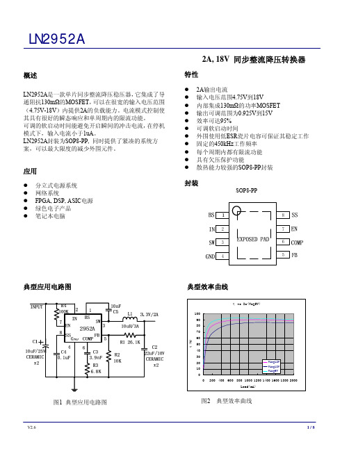
L N 2952A2A, 18V 同步整流降压转换器概述LN2952A是一款单片同步整流降压稳压器,它集成了导通阻抗130mΩ的MOSFET,可以在很宽的输入电压范围(4.75V-18V)内提供2A的负载能力。
电流模式控制使其具有很好的瞬态响应和单周期内的限流功能。
可调的软启动时间能避免开启瞬间的冲击电流,在停机模式下,输入电流小于1uA。
LN2952A封装为SOP8-PP, 同时提供了紧凑的系统方案,可以最大限度的减少外围元件。
应用z分立式电源系统z网络系统z FPGA, DSP, ASIC电源z绿色电子产品z笔记本电脑特性z2A输出电流z输入电压范围4.75V到18Vz内部集成130mΩ的功率MOSFETz输出可调范围为0.925V到15Vz效率可达95%z可调软启动时间z外围使用低ESR瓷片电容可保证其稳定工作z固定的450kHz工作频率z每个周期内都有限流功能z具有欠压保护功能z散热能力较强的SOP8-PP封装封装SOP8-PP典型应用电路图图1 典型应用电路图典型效率曲线η vs Io(Vo=5V)图2 典型效率曲线引脚说明引脚序号引脚名称引脚描述1 BS 上管栅极驱动升压输入。
BS为上管N沟道MOSFET开关提供驱动。
从SW到BS 端连接一个0.01uF或更大的电容。
2 IN 电源输入。
为IC以及降压转换器开关提供输入电源。
在4.75V至18V的电压范围驱动IN。
通过一个适当的大电容旁路IN到地,以消除输入IC的噪声。
3 SW 功率开关输出。
SW为开关节点提供电源输出。
从SW端到输出负载连接输出LC 滤波器。
请注意,从SW到BS需要接一个电容。
4 GND电源地(连接裸露焊盘到4引脚)。
5 FB 反馈输入端。
FB感应输出电压来调节这个电压。
通过来自输出电压的一个电阻分压器驱动FB。
反馈阈值电压是0.925V。
6 COMP 补偿节点。
COMP用来补偿调节控制回路。
从COMP脚到GND连接一个RC网络来补偿调节控制回路。
24V转5V降压芯片,24V转3.3V的稳压芯片,中文规格书
过电流保护和短路 当电感器电流峰值超过设置电流限制阈值。同时,输出电压开始下降,直到 FB 低于欠电压 (UV)阈值,通常低于参考值 25%。一旦一个紫外线被触发,就会进入打嗝模式以定期重 新启动部件。当输出为对地完全短路。平均短路电流大大降低,以减轻热并保护监管者。一 旦过电流情况出现,则退出 hiccup 模式远离的。
特征
⚫ 宽 4V 至 30V 工作输入范围 ⚫ 1.2A 连续输出电流 ⚫ 1.4MHz 开关频率 ⚫ 短路保护模式 ⚫ 内置过流限制 ⚫ 内置过电压保护 ⚫ 力模式 PWM ⚫ 内部软启动 ⚫ 200mΩ/150mΩ低 RDS(ON)内部功率金氧半电晶体 ⚫ 0.8V 输出可调 ⚫ 不需要肖特基二极管 ⚫ 综合内部补偿 ⚫ 热关机 ⚫ 提供 SOT23-6 套装 ⚫ -40°C 至+85°C 温度范围
绝对最大额定值(注 1/2)
VIN,EN,电压
-0.3Vto36V
VFB 电压
工作温度范围 铅温度(焊接,10s) ESD(人体制造)HMB VSW 电压 VBS 电压 储存温度范围 结温 ESD(机械制造)MM RθJA RθJC 注: (1) 超过这些额定值可能会损坏设备。 (2) 不能保证设备在其工作条件外正常工作。
误差放大器 误差放大器将 FB 引脚电压与内部 FB 基准(VFB)进行比较,并输出 a 电流与两者之差成正 比。该输出电流随后用于充电或放电内部补偿网络,这是用来控制功率 MOSFET 电流。优化 后的内部补偿网络使外部元件的数量和简化了控制回路设计。
内部软启动 软启动是为了防止变频器输出电压在启动。当芯片启动时,内部电路产生一个软启动电压 (SS)上升从 0V 到 0.807V。当低于内部参考(REF)时,SS 覆盖 REF,因此错误发生放大器 以 SS 为基准。当 SS 高于 REF 时,REF 恢复控制。时间就是时间内部最大为 1.2ms。