TD2776 同步降压芯片
uc2706dw电路工作原理

uc2706dw电路工作原理UC2706DW是一种常见的电路芯片,它具有广泛的应用领域。
在本文中,我将介绍UC2706DW电路的工作原理。
UC2706DW是一款高性能电流模式控制器。
它主要用于直流-直流(DC-DC)转换器的控制,可以实现高效的能量转换。
UC2706DW采用了电流模式控制的方式,通过监测电流信号来实现对输出电压的稳定控制。
UC2706DW的主要工作原理是通过内部的比较器来监测电流信号,并将其与参考电压进行比较。
当电流信号超过参考电压时,控制器会发出一个控制信号,调整开关管的导通时间,以达到稳定输出电压的目的。
UC2706DW还具有一些其他特性,例如内部的振荡器和误差放大器。
振荡器用于产生一定频率的脉冲信号,控制开关管的开关时间。
误差放大器用于放大电流信号和参考电压之间的差异,以便进行比较和控制。
在实际应用中,UC2706DW常用于DC-DC转换器中的开关电源设计。
开关电源是一种将输入电压转换为所需输出电压的电力转换装置。
通过使用UC2706DW电路,可以实现高效、稳定的能量转换,提高电源的效率和可靠性。
UC2706DW电路的工作原理可以总结为以下几个步骤:1. 输入电压经过整流和滤波电路后,进入DC-DC转换器。
2. UC2706DW电路监测输出电流,并与参考电压进行比较。
3. 如果输出电流超过参考电压,UC2706DW会发出一个控制信号。
4. 控制信号经过一定的延迟后,控制开关管的导通时间。
5. 开关管导通时,输入电压通过变压器传递到输出端,实现能量转换。
6. 控制信号的延迟时间和导通时间的调整,使输出电压稳定在设定值附近。
UC2706DW电路的工作原理基于电流模式控制的思想,通过对电流信号的监测和调整,实现对输出电压的精确控制。
这种控制方式具有快速响应、稳定性好等优点,广泛应用于各种电力转换系统中。
UC2706DW是一款高性能的电流模式控制器,通过对电流信号的监测和调整,实现对输出电压的稳定控制。
XL7026 降压型直流电源变换器芯片(高电压型)

Rev 1.0
0755-82543821 10
0.6A150KHz100V降压型DC-DC转换器
特点
12V至90V工作电压范围 最大占空比100% 最小压降0.5V 输出电压从1.25V至20V可调 5V输出时最大0.6A输出电流 15V输出时最大0.3A输出电流 固定150KHz开关频率 最大输出功率小于5W 内置高压功率MOSFET 效率高达85% 出色的线性与负载调整率 内置限流功能 内置输出短路保护功能 SOP8-EP封装
0.15
0.20
0.25
0.30
Output current(A)
图 8. XL7026 系统效率曲线
Rev 1.0
0755-82543821 7
XLSEMI
0.6A150KHz100V降压型DC-DC转换器 系统典型应用(VOUT=5V,IOUT=0~0.6A)
Datasheet XL7026
图 9. XL7026 系统参数测量电路(VIN=12V~90V,VOUT=5V,IOUT=0~0.6A)
应用
电动车控制器供电 通信
Rev 1.0
图 1. XL7026 封装
0755-82543821 1
XLSEMI
0.6A150KHz100V降压型DC-DC转换器 引脚配置
Datasheet XL7026
背部焊盘为SW
表 1.引脚说明
图 2. XL7026 引脚配置
引脚号 1
2 3
4 5,6 7 8
参数输入电压符号vin条件最小值典型值最大值单位129011输入欠压保护电压芯片供电引脚电压静态电源电流vinuvlovregiq102vfb25ma振荡频率foscil120xlsemidatasheetxl702606a150khz100v降压型dcdc转换器xl7026电气特性符号150180khzfb开关电流限值0667r3015mos导通电阻rdson180100210mohmiout03a最大占空比dmax0vfbrev10075582543821xlsemidatasheetxl702606a150khz100v降压型dcdc转换器典型性能特性quiescentsupplycurrentvstemperaturevin48v5025255075100125temperature静态电流曲线feedbackvoltagechangevstemperature302520vin48vvout5viout01anormalizedta25151005000510152025305025255075100125temperature反馈电压变化曲线rev10075582543821xlsemidatasheetxl702606a150khz100v降压型dcdc转换器系统典型应用vout15viout003axl7026系统参数测量电路vin16v90vvout15viout003aefficiencyvsoutputcurrent100959085807570656055vin24vvout15viout01a03avin36vvout15viout01a03a50454035302520vin48vvout15viout01a03avin60vvout15viout01a03avin72vvout15viout01a03avin84vvout15viout01a03a010015020025030outputcurrentaxl7026系统效率曲线rev10075582543821xlsemidatasheetxl702606a150khz100v降压型dcdc转换器系统典型应用vout5viout006axl7026系统参数测量电路vin12v90vvout5viout006aefficiencyvsoutputcurrent908580757065605550454035302520vin12vvo
平芯微PW2057降压芯片PDF规格书

SOT23-6 SOP8-EP SOP8-EP SOT23-6 SOP8-EP SOP8-EP SOP8-EP SOP8-EP SOP8 封装 SOT23-3
Sot23-3 Sot23/89 Sot23-3
PCB 布局建议
在布置印刷电路板时,应进行以下检查,以确保 PW2057 正常工作。在布局中检查以下内 容: 1 功率记录道,包括 GND 记录道、SW 记录道和 Vin 记录道短,直,宽。 2 将输入电容器尽可能靠近设备引脚(VIN 和 GND)。 3 开关节点电压波动较大,应保持小面积。使模拟组件远离 SW 节点,以防止杂散电容噪 声拾取。 4 将所有模拟接地连接到命令节点,然后将命令节点连接到输出电容器后面的电源接地。 5 尽可能靠近 CIN 和 COUT 的(-)板
PW2057
VOUT 也会增加波纹电流,如等式所示。设置纹波电流的合理起点是 I△L=280mA (700mA 的 40%)。
电感器的直流电流额定值应至少等于最大负载电流加上一半纹波电流,以防止铁芯饱和。 因此,对于大多数应用(700 毫安+140 毫安),一个 840 毫安额定电感器就足够了。为 了提高效率,选择低直流电阻电感。 不同的磁芯材料和形状会改变电感的尺寸/电流和价格/电流关系。铁氧体或坡莫合金材料 中的环形或屏蔽盆形磁芯体积小,辐射的能量不多,但通常比具有类似电气特性的粉末铁 芯电感器成本高。选择哪种类型的电感器通常更多地取决于价格和尺寸要求以及任何辐射 场/EMI 要求,而不是 PW2057 需要什么操作。
1.2V1.5V,1.8V,2.0V,2.5, .2.8V,3.0V,3.3V,5V 3V,3.3V,5V 3V,3.3V,5V 3V,3.3V,5V
杭州低压差线性稳压芯片型号
杭州低压差线性稳压芯片型号什么是低压差线性稳压芯片?低压差线性稳压芯片是一种电子元器件,它可以通过控制电流或电压,使电路获得稳定的压力。
它可以有效提高电子设备和系统的稳定性,同时也是很受电子工程师们青睐的一种电子器件。
杭州低压差线性稳压芯片型号1、LT3085型:它具有1000V/M的输入电阻,可提供4.6V的最小工作电压,支持600mA的负载电流,即使在最高2V工作电压下也具有良好的线性稳定性。
2、LT3086型:它具有较低的耗散功率,可提供4.4V的最小工作电压,最大可支持4A的负载电流,抗干扰特性非常突出,可以获得出色的线性稳定性。
3、LT3091型:它的输入电压为12V,最小工作电压为10V,支持3A的负载电流,提供适应性的负载模式,准确实现用户期望的稳定性。
4、LT3092型:它的输入电压可高达20V,最小的工作电压可达16V,支持2A的负载电流,芯片具有优异的热和电性能,且配备有电流限制功能,可提供更高级的性能。
5、LT3093型:它具有较大的输入电容,可提供3.3V的最小工作电压,最大可支持2A的负载电流,芯片具有良好的耐温性、耐压性,在较低压差下仍能实现可靠的线性稳压性能。
6、LT3094型:它具有极低的输出静态电流,可提供3V的最小工作电压,支持1.5A的负载电流,并且具有非常稳定的稳压特性,可以满足工业类应用中的各种复杂环境要求。
7、LT3095型:它有极低的输出静态电流,可提供2.5V的最小工作电压,支持2A的负载电流,芯片具有非常低的温度系数,可以实现高精度的线性稳压性能。
8、LT3097型:它具有低对称性,可提供2.2V的最小工作电压,支持1.6A的负载电流,芯片具有优异的电流限制特性,可以提供可靠的稳压特性。
综上所述,杭州的低压差线性稳压芯片型号有LT3085、LT3086、LT3091、LT3092、LT3093、LT3094、LT3095和LT3097等,它们在提供稳定性和准确稳压性能上都表现出色,在电子设备和系统中应用得广泛,是电子工程师们经常选择的一种元器件。
XL2576降压型直流电源变换器芯片(常规型)
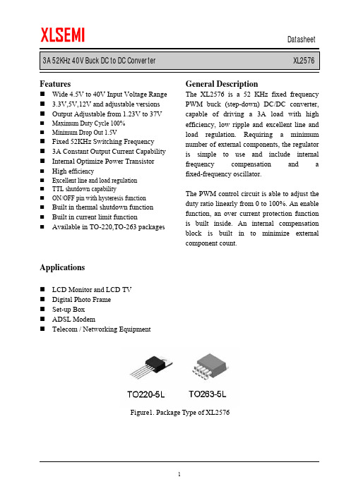
Figure3. Function Block Diagram of XL2576
Typical Application Circuit
Figure4. XL2576 Typical Application Circuit 12V-5V/3A
XL2576
System parameters test circuit figure6 VOUT Efficiency Output Voltage Vin = 4.75V to 40V Iload=0.2A to 3A Vin=12V ,Vout=3.3V Iout=3A 3.168 3.3 75 3.432 V %
Fixed 52KHz Switching Frequency 3A Constant Output Current Capability Internal Optimize Power Transistor High efficiency
Excellent line and load regulation TTL shutdown capability ON/OFF pin with hysteresis function
4
Datasheet 3A 52KHz 40V Buck DC to DC Converter Absolute Maximum Ratings(Note1)
Parameter Input Voltage Feedback Pin Voltage ON/OFF Pin Voltage Output Switch Pin Voltage Power Dissipation Thermal Resistance (TO220 & TO263) (Junction to Ambient, No Heatsink, Free Air) Operating Junction Temperature Storage Temperature Lead Temperature (Soldering, 10 sec) ESD (HBM) Symbol Vin VFB VON/OFF VOutput PD RJA TJ TSTG TLEAD Value -0.3 to 45 -0.3 to Vin -0.3 to Vin -0.3 to Vin Internally limited 30 -40 to 125 -65 to 150 260 >2000 Unit V V V V mW ºC/W ºC ºC ºC V
基准电源常用芯片
基准电源常用芯片
基准电源芯片(也称作电压基准源或参考电压源)是电子电路中用于提供精确、稳定且温度系数极低的固定输出电压的集成电路。
这类芯片在许多需要高精度和长期稳定的系统中扮演着重要角色,例如仪表仪器、数据转换器(ADC/DAC)、电源管理以及各类精密模拟电路。
以下是一些常见的基准电压芯片:
1. LM236系列:
LM236D-2.5, LM236DR-2.5, LM236LP-2.5:这些是Texas Instruments(TI)生产的2.5V基准电压源芯片,具有较宽的工作电流范围(400uA~10mA)。
2. LM285系列:
LM285D-1.2, LM285D-2.5, LM285LP-2.5:这些是微功耗电压基准芯片,适用于电流需求较低的应用,工作电流范围为10uA至20mA。
3. LM336系列:
LM336BD-2.5:同样是TI的一款2.5V基准电压源,具有与LM285类似的微功耗特性,工作电流也在10uA至20mA之间。
4. 其他典型基准电压芯片:
MC1403:摩托罗拉(现NXP)生产的2.5V基准电压源。
TL431:一个精密可调基准稳压源,其输出电压可在2.5V至36V范围内调节,广泛应用于各种电源控制和保护电路中。
AZ431BN-ATRE1:可能是ADI公司的一款高精度电压基准芯片。
FP6276A最新中文规格书
特征
电流模式,带 PWM/PSM 控制 输入电压范围:2.4V~4.5V 关机电流:<1uA 振荡器频率:500KHz 参考电压:0.6V+/-2% 停机期间断开负载 循环电流限制在 低 RDS(on):低压侧 55mΩ,高压侧 55mΩ。 保护:OTP、输出 OVP、OCP、SCP 内部补偿 内部软启动:7ms
软启动功能 软启动电路集成在 FP6276A 中,以避免上电时的浪涌电流。IC 后启用时,
错误放大器的输出被内部软启动功能钳制,这导致脉宽调制脉冲宽度缓慢增加, 从而减少输入浪涌电流。
电流限制程序 OC 和 GND 引脚之间的电阻编程峰值开关电流。电阻值应为在 37.5k 和 300k
之间。电流限值将从 5 A 设置为 0.8A。保持此针脚处的迹线尽可能短尽可能的。 不要把电容放在这个引脚上。根据下式:
包装:SOP8(EP)
应用
芯片
充电器 手持设备 便携式产品 电力银行
135 代 2845 理 8039 Mr。郑,工程 FAE
ห้องสมุดไป่ตู้ 典型应用电路
FP6276A
功能描述
FP6276A
操作 FP6276A 是一种电流模式同步升压转换器。恒定开关频率为 500 kHz,使用
脉冲宽度调制(PWM)工作。内置 50mΩ高压侧开关和 50mΩ低压侧开关提供 高效转换。
建议使用 X5R 和 X7R 陶瓷电容器低等效串联电阻(ESR)和更宽的工作温度范围。 输出电压编程
输出电压由电阻分压器从输出电压设置到 FB。输出电压为:
FP6276A
布局注意事项 1 功率跟踪,包括 GND 跟踪、LX 跟踪和 VIN 跟踪应保留短,直,宽。 2. LX 和 L 开关节点,宽而短的轨迹以减少 EMI。 3. 将 CIN 尽可能靠近 VIN 引脚,以保持输入电压稳定并过滤掉脉冲输入电
微功耗、低电压监测器MIC2776
微功耗、低电压监测器MIC2776
方佩敏
【期刊名称】《国外电子元器件》
【年(卷),期】2001(000)008
【摘要】MIC2776是MICREL公司推出的一款低电压电源监测器,可rn用来监测μC或μP电源电压(或电池电压)。
该器件在上电时rn,若电源电压正常,可输出上电复位信号。
而在电源电压rn低于设定的阈值电压时,可输出低电压复位信号。
另外,rnMIC2776还具有手动复位功能。
文中介绍了MIC2776的管脚功能rn、内部结构及工作原理,并给出了典型应用电路图。
【总页数】3页(P30-32)
【作者】方佩敏
【作者单位】北京航空航天大学
【正文语种】中文
【中图分类】TM933
【相关文献】
1.低电压微功耗电磁流量计测量原理分析 [J], 王尚宏;隋韶阳;郭永涛
2.微功耗电压监测器AN051的应用 [J], 方佩敏;胡伟生
3.低电压微功耗遥控模拟鼠标的设计 [J], 赵合运;赖振讲
4.Zetex推出崭新微功耗电流监测器 [J],
5.环保节能的低电压微功耗电磁流量计 [J], 王尚宏
因版权原因,仅展示原文概要,查看原文内容请购买。
基于I2C总线的多路负载电流及功率测量模块的设计与实现
基于I2C总线的多路负载电流及功率测量模块的设计与实现作者:姜涵来源:《电脑知识与技术》2015年第23期摘要:该文介绍了I2C总线技术在负载的电流功率采集测量中的应用,并针对I2C的技术特点和电气特征进行了分析。
同时介绍了I2C总线接口的芯片,电流/功率监控芯片 INA220,并给出了测量模块的系统结构设计原理。
关键词:I2C总线;电流/功率监控;INA220;ZLG7290中图分类号:TP336 文献标识码:A 文章编号:1009-3044(2015)23-0139-021 I2C总线I2C总线是双向、两线(SCL、SDA)、串行、多主控(multi-master)接口标准。
在它的协议体系中,传输数据时都会带上目的设备的设备地址,其地址由软件给定,称为主控制器的从地址。
一般具有I2C总线的器件的SCL和SDA引脚都是集电极开路的输出结构,因此在实际应用中,SCL和SDA信号线都必须加上3~10K左右的上拉电阻。
多个具有I2C总线接口的器件可以连接在同一条I2C总线上,彼此之间通过不同的从地址区分,总线上不需要额外的地址译码器,主设备一般为微处理器,首先根据从设备的地址字节为其指定地址,一般包括7个地址位和1个操作位(R/~W),操作位用于表示后续的操作是读还是写。
2 INA220概述INA220芯片是由美国TI(德州仪器)公司生产的一款电流及功率监控器,带有双线接口,可以同时监控电流路径和总线电压,总线电压范围在0~26V,器件供电电压为3.3V~5V,内置乘法寄存器,可以将测得的功率和电流以瓦特和安培为单位输出。
对主从总线兼容,双线协议和主从协议互相之间也可以兼容,能够提供数字电路的功率、电流及电压的采集测量,并可设定校准值以满足一定的精度要求。
2.1 INA220芯片特性INA220带有I2C总线接口,通过两条漏极是开路形式的双向线路SCL和SDA连接到总线,并由主设备(一般为CPU)对其进行初始化。
LM22677中文
开关频率为500kHz时,典型的最大占空比为90%。这对应200ns的 典型最小关断时间。工作在高于500kHz的开关频率时,200ns的最 小关断时间会使最大占空比减小到90%以下。为了在每个周期中给 自举电容器提供足够的充电时间,这个强制关断时间就很重要。
保证正常工作的最低输入电压是:
LM22677-5.0
VFB
反馈电压
LM22677-ADJ
VFB
反馈电压
所有输出电压版本
IQ ISTDBY
ICL IL
静态电流 待机静态电流 电流限制 输出漏电流
R DS(ON) fO
T OFFMIN T ONMIN
IBIAS VEN VENHYST
开关导通电阻 振荡器频率 最小关断时间 最小导通时间 反馈偏置电流 使能阈值电压 使能电压阈值滞后
封装
■ TO-263薄型(裸露焊盘)
应用领域
■ 工业控制 ■ 电信和数据通信系统 ■ 嵌入式系统 ■ 汽车行动通讯系统和车身电子装置 ■ 标准24V、12V和5V输入转换
应用原理简图
30074101
本文是National Semiconductor英文版的译文,本公司不对翻译中存在的差异或由此产生的错误负责。如需确认任何内容的准确性,请参考本公司提供的英 文版。
© 2010 美国国家半导体
300741
LM22677
连线图
订购信息
输出电压 ADJ ADJ 5.0 5.0
订购号 LM22677TJE-ADJ LM22677TJ-ADJ LM22677TJE-5.0
LM22677TJ-5.0
裸露焊盘 连接到GND 7引脚塑料TO-263薄型封装
- 1、下载文档前请自行甄别文档内容的完整性,平台不提供额外的编辑、内容补充、找答案等附加服务。
- 2、"仅部分预览"的文档,不可在线预览部分如存在完整性等问题,可反馈申请退款(可完整预览的文档不适用该条件!)。
- 3、如文档侵犯您的权益,请联系客服反馈,我们会尽快为您处理(人工客服工作时间:9:00-18:30)。
General DescriptionThe TD2776 is a monolithic synchronous buckregulator. The device integrates two 90m Ω MOSFETs, and provides 2.2A of continuous load current over a wide input voltage of 4.75V to 32V. Current mode control provides fast transient response and cycle-by-cycle current limit.An adjustable soft-start prevents inrush current at turn-on, and in shutdown mode the supply current drops to 1µA.This device, available i n an SOP8-PP package, provides a very compact solution with minimal external components.Features• 2.2A Output Current• Wide 4.75V to 32V Operating Input Range• Integrated 90m ΩPower MOSFET Switches• Output Adjustable from 0.923V to 30V• Up to 93% Efficiency• Programmable Soft-Start• Stable with Low ESR Ceramic Output Capacitors• F ixed 340KHz• Cycle-by-Cycle Over Current Protection• Input Under Voltage LockoutApplications• Distributed Power Systems • Networking Systems• FPGA, DSP, ASIC Power Supplies• Green Electronics/ Appliances• Notebook ComputersPackage TypesFigure 1. Package Types of TD2776Pin ConfigurationsFigure 2 Pin Configuration of TD2776(Top View) Pin DescriptionOrdering InformationTD2776 □□Circuit Type Packing:Blank:TubeR:Type and Reel PackageM:SOP8-PPFunction BlockFigure 3 Function Block Diagram of TD2776Absolute Maximum RatingsElectrical Characteristics V IN = 12V, T a = 25℃unless otherwise specified.Electrical Characteristics(Cont.)V IN = 12V, T a = 25℃unless otherwise specified.Typical Performance CharacteristicsFigure 4. Steady State Test Figure 5Startup through EnableFigure 6Startup through Enable Figure7. Shutdown through EnableFigure 8. Shutdown through EnableFigure 9 Load Transient TestFigure 10. Short Circuit TestFigure 11.Short Circuit RecoveryTypical Application CircuitFig13. TD2776 with 5V Output, 470µF/16V Electrolytic Output CapacitorFunction Description Component SelectionSetting the Output VoltageThe output voltage is set using a resistive voltage divider from the output voltage to FB pin.The voltage divider divides the output voltage down to the feedback voltage by the ratio:Where V FB is the feedback voltage and V OUT is the output voltage.Thus the output voltage is:R1+R2 can be as high as 1kΩ.InductorThe inductor is required to supply constant current to the output load while being driven by the switched input voltage. A larger value inductor will result in less ripple current that will result in lower output ripple voltage. However,the larger value inductor will have a larger physical size, higher series resistance, and/or lower saturation current. A good rule for determining the inductance to use is to allow the peak-to-peak ripple current in the inductor to be approximately 30% of the maximum switch current limit. Also, make sure that the peak inductor current is below the maximum switch current limit. The inductance value can be calculated by:Where V OUT is the output voltage, V IN is the input voltage, f S is the switching frequency, and ΔI L is the peak-to-peak inductor ripple current.Choose an inductor that will not saturate under the maximum inductor peak current. The peak inductor current can be calculated by:Where I LOAD is the load current.The choice of which style inductor to use mainly depends on the price vs. size requirements and anyEMI requirements.Optional Schottky DiodeDuring the transition between high-side switch and low-side switch, the body diode of the lowside power MOSFET conducts the inductor current. The forward voltage of this body diode is high. An optional Schottky diode may be paralleled between the SW pin and GND pin to improve overall efficiency. Table 1 lists example Schottky diodes and their Manufacturers.The input current to the step-down converter is discontinuous, therefore a capacitor is required to supply the AC current to the step-down converter while maintaining the DC input voltage. Use low ESR capacitors for the best performance. Ceramic capacitors are preferred, but tantalum or low-ESR electrolytic capacitors may also suffice. Choose X5R or X7R dielectrics when using ceramic capacitors.Since the input capacitor (C1) absorbs the inputswitching current it requires an adequate ripple current rating. The RMS current in the input capacitor can be estimated by: The worst-case condition occurs at V IN = 2V OUT ,where I C1 = I LOAD /2. For simplification, choose the inputcapacitor whose RMS current rating greater than half of the maximum load current.The input capacitor can be electrolytic, tantalum or ceramic. When using electrolytic or tantalumcapacitors, a small, high quality ceramic capacitor, i.e.0.1μF, should be placed as close to the IC as possible.When using ceramic capacitors, make sure that they have enough capacitance to provide sufficient charge to prevent excessive voltage ripple at input. The input voltage ripple for low ESR capacitors can be estimated by:Where C1 is the input capacitance value. Output CapacitorThe output capacitor is required to maintain the DC output voltage. Ceramic, tantalum, or low ESRelectrolytic capacitors are recommended. Low ESR capacitors are preferred to keep the output voltage ripple low. The output voltage ripple can be estimated by:Where C2 is the output capacitance value and R ESR is the equivalent series resistance (ESR) value of the output capacitor.In the case of ceramic capacitors, the impedance at the switching frequency is dominated by the capacitance. The output voltage ripple is mainly caused by the capacitance. For simplification, the output voltage ripple can be estimated by:In the case of tantalum or electrolytic capacitors,the ESR dominates the impedance at the switchingfrequency. For simplification, the output ripple can be approximated to:The characteristics of the output capacitor also affect the stability of the regulation system. The TD2776 can be optimized for a wide range of capacitance and ESR values.Compensation ComponentsTD2776 employs current mode control for easy compensation and fast transient response. Thesystem stability and transient response are controlled through the COMP pin. COMP pin is the output of the internal transconductance error amplifier. A series capacitor-resistor combination sets a pole-zerocombination to control the characteristics of the control system.The DC gain of the voltage feedback loop is given by:Where A VEA is the error amplifier voltage gain;G CS is the current sense transconductance and R LOAD is the load resistor value.The system has two poles of importance. One is due to the compensation capacitor (C3) and the output resistor of the error amplifier, and the other is due to the output capacitor and the load resistor. These poles are located at:Where G EA is the error amplifier transconductance.The system has one zero of importance, due to the compensation capacitor (C3) and the compensationresistor (R3). This zero is located at:The system may have another zero of importance, if the output capacitor has a large capacitance and/or a high ESR value. The zero,due to the ESR and capacitance of the output capacitor, is located at:In this case (as shown in Figure 14), a third pole set bythe compensation capacitor (C6) and the compensation resistor (R3) is used to compensate theeffect of the ESR zero on the loop gain. This pole is located at:The goal of compensation design is to shape theconverter transfer function to get a desired loop gain. The system crossover frequency where the feedback loop has the unity gain is important. Lower crossover frequencies result in slower line and load transient responses,while higher crossover frequencies could cause system instability. A good rule of thumb is to set the crossover frequency below one-tenth of the switching frequency.To optimize the compensation components, the following procedure can be used.1. Choose the compensation resistor (R3) to set the desired crossover frequency.Determine the R3 value by the following equation:Where f C is the desired crossover frequency which is typically below one tenth of the switching frequency.2. Choose the compensation capacitor (C3) to achieve the desired phase margin. For applications with typicalinductor values, setting the compensation zero, f Z1, below one-forth of the crossover frequency provides sufficient phase margin.Determine the C3 value by the following equation:Where R3 is the compensation resistor.3. Determine if the second compensation capacitor (C6) is required. It is required if the ESR zero of the output capacitor is located at less than half of the switching frequency, or the following relationship is valid:If this is the case, then add the second compensationcapacitor (C6) to set the pole f P3 at the location of the ESR zero. Determine the C6 value by the equation: External Bootstrap DiodeAn external bootstrap diode may enhance the efficiency of the regulator, the applicable conditions of external BST diode are: ● V OUT =5V or 3.3V; and ● Duty cycle is high: In these cases, an external BST diode isrecommended from the output of the voltage regulator to BST pin, as shown in Fig.14Figure14.Add Optional External Bootstrap Diode to EnhanceEfficiencyThe recommended external BST diode is IN4148, andthe BST cap is 0.1~1μF.Package InformationSOP8-pp Package Outline Dimensions。