STM32F0-DISCOVERY用户手册
STM32F429 Discovery 用户手册说明书
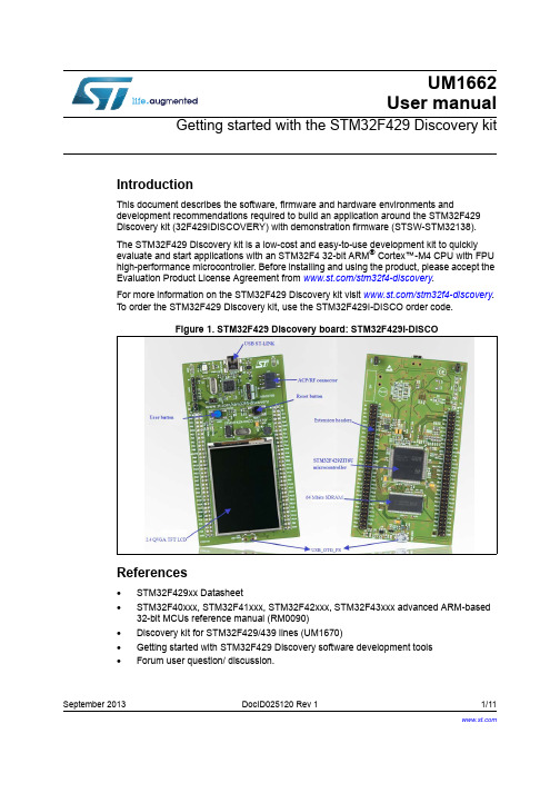
September 2013DocID025120 Rev 11/11UM1662User manualGetting started with the STM32F429 Discovery kitIntroductionThis document describes the software, firmware and hardware environments anddevelopment recommendations required to build an application around the STM32F429 Discovery kit (32F429IDISCOVERY) with demonstration firmware (STSW-STM32138).The STM32F429 Discovery kit is a low-cost and easy-to-use development kit to quickly evaluate and start applications with an STM32F4 32-bit ARM ® Cortex™-M4 CPU with FPU high-performance microcontroller. Before installing and using the product, please accept the Evaluation Product License Agreement from /stm32f4-discovery .For more information on the STM32F429 Discovery kit visit /stm32f4-discovery . To order the STM32F429 Discovery kit, use the STM32F429I-DISCO order code.Figure 1. STM32F429 Discovery board: STM32F429I-DISCOReferences•STM32F429xx Datasheet•STM32F40xxx, STM32F41xxx, STM32F42xxx, STM32F43xxx advanced ARM-based 32-bit MCUs reference manual (RM0090)•Discovery kit for STM32F429/439 lines (UM1670)•Getting started with STM32F429 Discovery software development tools •Forum user question/ discussion.Contents UM1662Contents1Hardware configuration and layout . . . . . . . . . . . . . . . . . . . . . . . . . . . . . 41.1Features . . . . . . . . . . . . . . . . . . . . . . . . . . . . . . . . . . . . . . . . . . . . . . . . . . . 41.2Microcontroller . . . . . . . . . . . . . . . . . . . . . . . . . . . . . . . . . . . . . . . . . . . . . . 41.3System requirement . . . . . . . . . . . . . . . . . . . . . . . . . . . . . . . . . . . . . . . . . . 51.4Powering up the board . . . . . . . . . . . . . . . . . . . . . . . . . . . . . . . . . . . . . . . . 51.5Reset the board . . . . . . . . . . . . . . . . . . . . . . . . . . . . . . . . . . . . . . . . . . . . . 61.6Hardware block diagram . . . . . . . . . . . . . . . . . . . . . . . . . . . . . . . . . . . . . . 62Firmware package . . . . . . . . . . . . . . . . . . . . . . . . . . . . . . . . . . . . . . . . . . . 72.1Package description . . . . . . . . . . . . . . . . . . . . . . . . . . . . . . . . . . . . . . . . . . 72.2Programming firmware application . . . . . . . . . . . . . . . . . . . . . . . . . . . . . . . 72.2.1Programming application . . . . . . . . . . . . . . . . . . . . . . . . . . . . . . . . . . . . . 82.2.2Run pre-loaded demo . . . . . . . . . . . . . . . . . . . . . . . . . . . . . . . . . . . . . . . 8 3Revision history . . . . . . . . . . . . . . . . . . . . . . . . . . . . . . . . . . . . . . . . . . . 102/11DocID025120 Rev 1UM1662List of figures List of figuresFigure 1.STM32F429 Discovery board: STM32F429I-DISCO . . . . . . . . . . . . . . . . . . . . . . . . . . . . . . 1 Figure 2.STM32F429I-DISCO power sources . . . . . . . . . . . . . . . . . . . . . . . . . . . . . . . . . . . . . . . . . . 7 Figure 3.Hardware block diagram. . . . . . . . . . . . . . . . . . . . . . . . . . . . . . . . . . . . . . . . . . . . . . . . . . . . 8 Figure 4.Package contents. . . . . . . . . . . . . . . . . . . . . . . . . . . . . . . . . . . . . . . . . . . . . . . . . . . . . . . . . 9 Figure 5.Hardware environnement. . . . . . . . . . . . . . . . . . . . . . . . . . . . . . . . . . . . . . . . . . . . . . . . . . 11DocID025120 Rev 13/111 Hardware configuration and layout1.1 FeaturesThe STM32F429 Discovery offers the following features:•STM32F429ZIT6 microcontroller featuring 2 MB of Flash memory, 256 KB of RAM in an LQFP144 package•On-board ST-LINK/V2 with selection mode switch to use the kit as a standalone ST-LINK/V2 (with SWD connector for programming and debugging)•Board power supply: through the USB bus or from an external 3 V or 5 V supply voltage•L3GD20, ST MEMS motion sensor, 3-axis digital output gyroscope•TFT LCD (Thin-film-transistor liquid-crystal display) 2.4", 262K colors RGB,240x320dots•SDRAM 64 Mbits (1Mbit x 16-bit x 4-bank) including an AUTO REFRESH MODE, anda power-saving•Six LEDs:–LD1 (red/green) for USB communication–LD2 (red) for 3.3 V power-on–Two user LEDs:LD3 (green), LD4 (red)–Two USB OTG LEDs:LD5 (green) VBUS and LD6 (red) OC (over-current)•Two pushbuttons (user and reset)•USB OTG with micro-AB connector•Extension header for LQFP144 I/Os for a quick connection to the prototyping board and an easy probing1.2 MicrocontrollerThe STM32F429ZIT6U device is based on the high-performance ARM® Cortex™-M4 32-bitRISC core operating at a frequency of up to 180 MHz The Cortex-M4 core features aFloating point unit (FPU) single precision which supports all ARM single-precisiondata-processing instructions and data types. It also implements a full set of DSP instructionsand a memory protection unit (MPU) which enhances application security.The STM32F429ZIT6U device incorporates high-speed embedded memories (2Mbytes ofFlash memory, 256 Kbytes of SRAM), up to 4 Kbytes of backup SRAM, and an extensiverange of enhanced I/Os and peripherals connected to two APB buses, two AHB buses anda 32-bit multi-AHB bus matrix.4/11DocID025120 Rev 1DocID025120 Rev 15/111.3 System requirement•Windows PC (XP , Vista, 7)•USB type A to Mini-B USB cable •ST-LINK/V2•Supported IDE are EWARM (IAR Embedded Workbench ®), MDK-ARM™ and AtollicTrueSTUDIO ®Note:Required information to download and install desired IDE and ST-LINK/V2 are detailed in Getting started with STM32F429 Discovery software development tools document.1.4 Powering up the boardThe STM32F429I-DISCO board can be powered up from three sources.•USB ST-LINK: To power the board from the USB connector CN1, use the 'USB type Ato Mini-B' cable and connect it between the host and the board USB connector CN1. •External sources: DC power supply can be inserted in the GND and 3V (or 5V) pin.Figure 2. STM32F429I-DISCO power sourcesUSB ST-LINK (CN1)5V 3V1.5 Reset the boardThere are three ways to reset the board:•Push the reset button mounted on the STM32F429I-DISCO.•Remove and reinsert the USB cable.•The MCU can also be reset by debuggers.1.6 Hardware block diagramThe STM32F429I-DISCO is designed around the STM32F429ZIT6U microcontroller in a144-pin LQFP package. Figure3 illustrates the connections between the STM32F429ZIT6Uand its peripherals (STLINK/V2, pushbutton, LED, USB and connectors).Please refer to schematic under /stm32f4-discovery for more details.6/11DocID025120 Rev 1DocID025120 Rev 17/11UM1662Firmware package2 Firmware packageTo get started with the STM32F429 Discovery kit, a firmware package that contains a set ofIP examples and demonstrations of some features exists under /stm32f4-discovery .2.1 Package descriptionThe STM32F429 Discovery firmware applications, demonstration and IPs examples areprovided in one single package and supplied in one single zip file. The extraction of the zip file generates one folder, STM32F429I-Discovery_FW_VX.Y.Z , which contains the following subfolders:Figure 4. Package contentsUser can run examples provided within this package. A set of examples for each peripheral are ready to be run.2.2 Programming firmware applicationTo start programming, user must:•Install preferred Integrated Development Environment (IDE)•Install the ST-LINK V2 driver from ST web siteFirmware package UM16628/11DocID025120 Rev 12.2.1 Programming applicationTo program application (demonstration or example), follow the sequence below:1.Go under application folder 2. Chose the desired IDE project3. Double click on the project file (ex. STM32F429I-Discovery_Demo.eww for EWARM)4. Rebuild all files: Project->Rebuild all5.Load project image: Project->Debug6. Run program: Debug->GoPlease refer to Getting started with STM32F429 Discovery software development toolsfor more details.2.2.2 Run pre-loaded demoTo run and develop any firmware applications on your STM32F429 Discovery board, theminimum requirements are as follows:–Windows PC (XP , Vista, 7)–‘USB type A to Mini-B' cable, used to power the board (through USB connector CN1) from host PC and connect to the embedded ST-LINK/V2 for debugging and Programming.Additional hardware accessories will be needed to run some applications:–‘USB type A to Micro-B' cable, used to connect the board (through USB connector CN5) as USB Device to host PC.DocID025120 Rev 19/11UM1662Firmware packageEstablish the connection with the STM32F429 Discovery board as follows:Figure 5. Hardware environnementThe demonstration software, based on the STemWin GUI library, is already preloaded in the board's Flash memory. It uses the LCD TFT mounted on the board to show the Menu based-on-icon view widget (Image Browser, Game, Performance, Clock/Calendar, Video and System Info module). The status bar indicate the CPU Usage, date, USB disk flash connection state, alarm and time.Follow the sequence below to configure the STM32F429 Discovery board and launch the DISCOVER application:1.Ensure that the jumpers JP3 and CN4 are set to "on" (Discovery mode).2.Connect the STM32F429 Discovery board to a PC using a USB cable type A/mini-B through the USB ST-LINK connector CN1, to power the board. The LEDs LD2 (PWR) and LD1 (COM).3.The following applications are available on the screen:–Clock/Calendar and Game–Video Player and Image Browser (play videos and view images from the USB mass storage connected to CN6)–Performance monitor (watch the CPU load and run a graphical benchmark)–System Info4. The demo software, as well as other software examples that allow you to discover the STM32 F4 series features, are available on /stm32f4-discovery .5.Develop your own applications starting from the examples.Revision history UM166210/11DocID025120 Rev 13 Revision historyTable 1. Document revision historyDate Revision Changes09-Sep-20131Initial release.UM1662Please Read Carefully:Information in this document is provided solely in connection with ST products. STMicroelectronics NV and its subsidiaries (“ST”) reserve the right to make changes, corrections, modifications or improvements, to this document, and the products and services described herein at any time, without notice.All ST products are sold pursuant to ST’s terms and conditions of sale.Purchasers are solely responsible for the choice, selection and use of the ST products and services described herein, and ST assumes no liability whatsoever relating to the choice, selection or use of the ST products and services described herein.No license, express or implied, by estoppel or otherwise, to any intellectual property rights is granted under this document. If any part of this document refers to any third party products or services it shall not be deemed a license grant by ST for the use of such third party products or services, or any intellectual property contained therein or considered as a warranty covering the use in any manner whatsoever of such third party products or services or any intellectual property contained therein.UNLESS OTHERWISE SET FORTH IN ST’S TERMS AND CONDITIONS OF SALE ST DISCLAIMS ANY EXPRESS OR IMPLIED WARRANTY WITH RESPECT TO THE USE AND/OR SALE OF ST PRODUCTS INCLUDING WITHOUT LIMITATION IMPLIED WARRANTIES OF MERCHANTABILITY, FITNESS FOR A PARTICULAR PURPOSE (AND THEIR EQUIVALENTS UNDER THE LAWS OF ANY JURISDICTION), OR INFRINGEMENT OF ANY PATENT, COPYRIGHT OR OTHER INTELLECTUAL PROPERTY RIGHT.ST PRODUCTS ARE NOT DESIGNED OR AUTHORIZED FOR USE IN: (A) SAFETY CRITICAL APPLICATIONS SUCH AS LIFE SUPPORTING, ACTIVE IMPLANTED DEVICES OR SYSTEMS WITH PRODUCT FUNCTIONAL SAFETY REQUIREMENTS; (B) AERONAUTIC APPLICATIONS; (C) AUTOMOTIVE APPLICATIONS OR ENVIRONMENTS, AND/OR (D) AEROSPACE APPLICATIONS OR ENVIRONMENTS. WHERE ST PRODUCTS ARE NOT DESIGNED FOR SUCH USE, THE PURCHASER SHALL USE PRODUCTS AT PURCHASER’S SOLE RISK, EVEN IF ST HAS BEEN INFORMED IN WRITING OF SUCH USAGE, UNLESS A PRODUCT IS EXPRESSLY DESIGNATED BY ST AS BEING INTENDED FOR “AUTOMOTIVE, AUTOMOTIVE SAFETY OR MEDICAL” INDUSTRY DOMAINS ACCORDING TO ST PRODUCT DESIGN SPECIFICATIONS. PRODUCTS FORMALLY ESCC, QML OR JAN QUALIFIED ARE DEEMED SUITABLE FOR USE IN AEROSPACE BY THE CORRESPONDING GOVERNMENTAL AGENCY.Resale of ST products with provisions different from the statements and/or technical features set forth in this document shall immediately void any warranty granted by ST for the ST product or service described herein and shall not create or extend in any manner whatsoever, any liability of ST.ST and the ST logo are trademarks or registered trademarks of ST in various countries.Information in this document supersedes and replaces all information previously supplied.The ST logo is a registered trademark of STMicroelectronics. All other names are the property of their respective owners.© 2013 STMicroelectronics - All rights reservedSTMicroelectronics group of companiesAustralia - Belgium - Brazil - Canada - China - Czech Republic - Finland - France - Germany - Hong Kong - India - Israel - Italy - Japan - Malaysia - Malta - Morocco - Philippines - Singapore - Spain - Sweden - Switzerland - United Kingdom - United States of AmericaDocID025120 Rev 111/11。
STM32F4Discovery 扩展板用户手册

STM32F407 Discovery ExtBoard用户手册版本 2011-05-01(本手册不断更新,建议您在官方网站下载最新版本)版权声明本手册版权归属天津淘淘科技电子有限公司(以下简称“淘淘科技”)所有, 并保留一切权力。
非经淘淘科技同意(书面形式),任何单位及个人不得擅自摘录本手册部分或全部,违者我们将追究其法律责任。
敬告:在售开发板的手册会经常更新,请在 网站查看最近更新,并下载最新手册,恕不再另行通知。
更新说明日期说明2012-05-01 本手册第一次发布目录1.1 STM32F407 Discovery ExtBoard开发板简介STM32F407 Discovery ExtBoard(下简称“本开发板”)是一款十分精致的低价高品质一体化STM32F407 Discovery CortexM4扩展开发板,由天津淘淘科技设计、生产和发行销售。
它采用STM32F407 Discovery作为核心板(下简称“核心板”),在设计上最大限度的贴近STM公司的开发板“精细”的风格,而且布局更加合理,接口更加丰富,十分适用于开发 MID、汽车电子、工业控制、导航系统、媒体播放等终端设备;也可适用于高校教学、嵌入式培训、个人研究学习和DIY 等。
具体而言,本开发板除了保留原有核心板的重力感应、三轴加速度传感器、miniUSB(A-B两种接口)、3.5mm 音频输出口、100PIN GPIO、LED、用户按键以外,本开发板还扩展了 LCD、4 线电阻触摸屏接口、100M 标准网络接口、DB9 串口、CAN总线接口、SD 卡接口、数字Camera接口,并为用户提供了AD 可调电阻等。
所有这些,都极大地方便了开发者的评估和使用,再加上我们按照本开发板尺寸专门定制的 LCD 模块,真正做到充分发挥STM官方原装开发板的强大功能。
我们还充分地发挥了原装开发板在线调试的ST-Link/v2,您不必再额外购买JTAG仿真器等调试设备,仅需要一根usb线就可以在尽情发挥CortexM4的特性。
芯达STM32用户使用手册
STM32F103VET6芯达 STM32○RUser's ManualPreliminaryRevision 1.0(2010.06.08) 芯达STM32开发板开发指南Copyright © 2009‐2010 ARM79 Limited. All rights reserved版本信息本手册进行了以下更改。
芯达STM32用户手册修订记录日期 修订版本 CR ID 修改章节 修改描述 作者 2010-5-28 1.00 全部 创建 林辰 2010-8-16 1.10 去掉蜂鸣器、AT45 林辰 2010-8-20 1.20 增加外扩接口、修林辰改外观图片版权声明本手册版权归属(以下简称“arm79”)所有, 并保留一切权力。
非经arm79同意(书面形式),任何单位或个人不得擅自摘录本手册部分或全部,违者我们将追究其法律责任。
敬告:在售开发板的手册会经常更新,请在网站查看最近更新,并下载最新手册,不再另行通知。
目录目录 (4)写在前面 (5)第一章芯达STM32光盘使用说明 (6)第二章芯达STM32硬件说明 (8)2.1 芯达STM32板载资源说明 (8)2.2 芯达STM32原理图说明 (9)2.2.1电源电路 (9)2.2.2 实时时钟(备用电池)电路 (9)2.2.3 系统时钟电路 (9)2.2.4 JTAG接口电路 (10)2.2.5 复位电路 (10)2.2.6 用户LED电路 (10)2.2.7 串口电路 (11)2.2.8 按键电路 (11)2.2.9 SD卡接口电路 (12)2.2.10 USB接口电路 (12)2.2.11 LCD TFT液晶接口电路 (13)2.2.12 外扩IO接口电路 (13)第三章芯达STM32开发前的准备 (15)3.1 J-Link驱动的安装 (15)3.2 使用J-Link下载调试 (18)3.3使用ISP下载调试 (25)3.3.1 安装Flash loader (25)3.3.2 使用ISP下载调试 (28)3.4安装RealView MDK软件 (34)3.5使用MDK + J-Link调试 (38)第四章芯达STM32初步开发举例 (49)4.1 下载固件库 (49)4.2 STM32简单开发 (50)附福州芯达工作室简介 (54)写在前面感谢您选购芯达STM32开发板产品!请详细阅读以下文字,以获取对芯达STM32开发板的更多信息。
STM32F051x4 STM32F051x6参考手册

■ Communication interfaces – Up to two I2C interfaces; one supporting Fast Mode Plus (1 Mbit/s) with 20 mA current sink, SMBus/PMBus, and wakeup from STOP
Datasheet − productre: ARM 32-bit Cortex™-M0 CPU, frequency up to 48 MHz
■ Memories – 16 to 64 Kbytes of Flash memory – 8 Kbytes of SRAM with HW parity checking
– One 16-bit timer with 1 IC/OC
– Independent and system watchdog timers
– SysTick timer: 24-bit downcounter
– One 16-bit basic timer to drive the DAC
■ Calendar RTC with alarm and periodic wakeup from Stop/Standby
– Up to two SPIs (18 Mbit/s) with 4 to 16 programmable bit frame, 1 with I2S interface multiplexed
– HDMI CEC interface, wakeup on header reception
■ Serial wire debug (SWD)
■ Up to 11 timers – One 16-bit 7-channel advanced-control timer for 6 channels PWM output, with deadtime generation and emergency stop – One 32-bit and one 16-bit timer, with up to 4 IC/OC, usable for IR control decoding
STM32开发板操作手册说明书
Heavy Duty Surface Mount TC 26881
Strapon® RTD Sensors 22391, 22392 & 22393
–200°C to +760°C (–320°F to +1400°F) Leads to 480°C (900°F)
To illustrate these points Figure I shows a typical surface sensor installation. The sensor in this case is mounted on a pipe which is carrying a fluid. The point closest to the fluid where a sensor can be mounted practically is the outer wall of the pipe. If the fluid flow is adequate and the temperature fluctuations are not severe, the outer wall temperature will be very close to that of the fluid.
–200°C to +232°C (–320°F to +450°F) –200°C to260°C (–320°F to +500°F)
Thermocouple Types K, E, T or J* Grounded or Ungrounded
Resistance 100 Ω or 1000 Ω Platinum @0°C
STM32F0DISCOVERY 开发板用户手册说明书
Open32F0-D User ManualContents1. Overview (2)1.1. What’s on board (2)2. Demo (4)2.1. 8IOs (4)2.2. 24L01 (5)2.3. ADC+DMA (5)2.4. DAC+DMA (6)2.5. FATFS V0.08A-SD Card (6)2.6. GPIO LED (7)2.7. GPIO LED JOYSTICK (7)2.8. I2C (7)2.9. I2S UDA1380 & SD_FatFS(DMA) (8)2.10. JOYSTICK (8)2.11. LCD22-picture (8)2.12. LCD22_TouchPanel (9)2.13. One-Wire (10)2.14. SPI (10)2.15. uCOS-II-V2.91 (11)2.16. uCOS-II-V2.91+LCD (11)2.17. USART (11)3. Revision history (12)1. Overview 1.1. What’s on board[ Core interface ]1. STM32F0DISCOVERY socketfor easily connecting theSTM32F0DISCOVERY2. 8I/Os + DAC + ADC interfacefor connecting accessory boards such buttons, motors, AD/DA module etc.3. USART2 interfaceeasily connects to RS232, RS485, USB TO232, etc.4. SPI1/SPI2 interface[ Other interface ]10. 5V/3.3V power input/outputusually used as power output, alsocommon-grounding with other user board11. 5V DC jack12. MCU pins connectorall the MCU I/O ports are accessible onexpansion connectors for further expansion 13. SWD interfacefor debugging/programmingeasily connects to SPI peripherals such asDataFlash (AT45DBxx), SD card, MP3 module, etc.5. LCD connectorfor connecting touch screen LCD 6.USART1 interfaceeasily connects to RS232, RS485, USB TO 232, etc.7.I2C1 / I2C2 interfaceeasily connects to I2C peripherals such as I/O expander (PCF8574), FRAM (FM24CLxx), etc. 8.I2S / I2C1 interfaceeasily connects to I2S peripherals such as audio module, etc. 9.1-WIRE interfaceeasily connects to ONE-WIRE devices (TO-92 package), such as temperature sensor (DS18B20), electronic registration number (DS2401), etc.[ Jumper/switch ] •Joystick jumpershort the jumper to connect the joystick to default I/Os used in example code;open the jumper to connect the joystick to custom I/Os via jumper wires14. Boot mode switchfor configuring BOOT0 pin.[ Component ] 15. Power switch 16. Power indicator17. Joystick: five positions2. DemoKEIL MDK Version :4.54Programmer/Debugger: STM32F0DISCOVERY onboard SWD Programming/Debugging interface: SWDSerial port settings:2.1. 8IOs◆ Overview8bit I/Os demo◆ Hardware connectionConnect the RS232 board to the onboardUSART1 interfaceConnect the 8 Push Button to the onboard 8I/Os connector (Make sure the G pinheader is connect to the board GND pinheader)◆ Operation and result◆The below information will be printed on the serial debugging assistantSelect a proper COM portBaud rate 115200Data bits 8Stop bits 1 Parity bitsNoneFlow control None2.2. 24L01◆ OverviewNRF24L01 demo ◆ Hardware connectionConnect the RS232 board to the onboardUSART1 interfaceConnect the two NRF24L01 to the board viaSPI interface ◆ Software configurationTwo NRF24L01 are needed for this demo, configuring as below:When configuring as sending mode, enable: #define T_O_R 1, comment out: //#define T_O_R 0 When configuring as receiving mode, enable: #define T_O_R 0, comment out: //#define T_O_R 0. ◆ Operation and resultMessage will be printed on the serial debugging assistant.2.3. ADC+DMA◆ OverviewADC+DMA demo◆ Hardware connectionConnect the RS232 board to the onboardUSART1 interfaceConnect the Analog Test Board to the board via8 I/Os (ADC+DAC)◆ Operation and resultRotate the onboard potentiometer, the AD message will be printed on the serial debugging assistant:2.4. DAC+DMA◆ OverviewDAC+DMA demo◆ Hardware connectionConnect the Analog Test Board to the board via8 I/Os (ADC+DAC)Connect the 5V pinheaders on both the mainboard and the Analog Test Board via jumper wire◆ Operation and resultYou may hear sound from the Analog Test Board when press the Reset button2.5. FATFS V0.08A-SD Card◆ OverviewSD_FatFS demo ◆ Hardware connectionConnect the RS232 board to the onboardUSART1 interfaceConnect the Micro SD Storage Board to theboard via SDIO interface.Insert the SD card to the Micro SD Storage Board socketConnect the CD pin on the Micro SD StorageBoard to the board PB0 pin via Dupont wire.`◆ Operation and resultThe below information will be printed on the serial debugging assistant:2.6. GPIO LED◆ OverviewLED demo◆ Hardware connection ◆ Operation and resultThe two LEDs on the Discovery board blinking2.7. GPIO LED JOYSTICK◆ OverviewUser key demo◆ Hardware connection ◆ Operation and resultPress the User key, the LED status will change accordingly.2.8. I2C◆ OverviewI2C EEPROM demo ◆ Hardware connectionConnect the RS232 board to the onboardUSART1 interfaceConnect the AT24/FM24 Board to theI2CX connector ( connect to I2C1 or I2C2 depends on the program)◆ Operation and resultThe below information will be printed on the serial debugging assistant:2.9. I2S UDA1380 & SD_FatFS(DMA)◆ OverviewAudio file placed on SD Card (with FATFS) ◆ Hardware connectionConnect Micro SD Storage Board to the board viaSPI2 interface.Insert the SD card to the Micro SD Storage Boardsocket. Connect the CD pin of the Micro SD Storage Boardto the board PB0 pin via DuPont wire. Put “audio.wav“ file to the SD cardConnect UDA1380 Board to the board via I2Sconnector.Connect the earphone to the UDA1380 Board viaLINEOUT interface.◆ Operation and resultYou can hear music while pressing the RESET key.2.10. JOYSTICK◆ OverviewJOYSTICK demo ◆ Hardware connectionShort the JOYSTICK JMP ◆ Operation and resultThe LED status will change accordingly while press the JOYSTICK .2.11. LCD22-picture◆ OverviewLCD demoThis LCD is 2.2 inch resistive touch screen LCD, the resolution is 320x240, drive by mode of SPI, greatlyreduce the pins, MCU with little IO can also available to drive it.This demo shows dot, the drawing line, the drawing circle, character, etc displayed on the LCD. ◆ Hardware connectionConnect with 5V power via the 5VDC interface Connect ULINK2 to the board via SWD interfaceConnect the 2.2inch 320x240 Touch LCD (A) to theboard via LCD22 interface.◆ Operation and resultMessage will be displayed on the LCD.2.12. LCD22_TouchPanel◆ OverviewLCD demo1. Calibrate the touch screen by click three times, and then enter into drawing board in the touch screeninterface.2. You can draw lines freely on the drawing board. ◆ Hardware connectionConnect the 2.2inch 320x240 Touch LCD (A) to the board. ◆ Operation and resultMessage will be displayed on the LCDTouch-screen calibration interface◆ ApplicationHandheld device display2.13. One-Wire◆ OverviewOne-Wire demo◆ Hardware connectionConnect the RS232 board to the onboard USART1 interface Connect the DS18B20 to the board via One-Wire interface◆ Operation and resultThe below information will be printed on the serial debugging assistant:2.14. SPI◆ OverviewSPI demo◆ Hardware connectionConnect the AT45DBXX DataFlash Board to theboard via SPIX (to SPI1 or SPI2 depends on the program)Connect the RS232 board to the onboard USART1interface◆ Software configurationThe serial debugging assistant configuring:Launch the serial debugging assistant SSCOM32, choose related COM port, set baud rate as 115200, click to open it.◆ Operation and resultThe below information will be printed on the serial debugging assistant:2.15. uCOS-II-V2.91◆OverviewuCOSII demo◆Hardware connection◆Operation and resultThe two LED blinking.2.16. uCOS-II-V2.91+LCD◆OverviewuCOS-II-V2.91I demo◆Hardware connectionConnect the 2.2inch 320x240 Touch LCD (A) to the board◆Operation and resultMessage displayed on the LCD; LED blinking.2.17. USART◆OverviewUSART demo◆Hardware connection◆Operation and resultThe below information will be printed on the serial debugging assistant:3. Revision historyVersion Description Date AuthorV1.0 Initial revision 2014/05/17 Waveshare team。
STM32F10x参考手册参考手册参考手册参考手册
关于如何进入停止模式,详见表 3-4。 在停止模式下,通过设置电源控制寄存器(PWR_CR)的 LPDS 位使内部调节器进入低功耗 模式,能够降低更多的功耗。
如果正在进行 Flash 编程,直到对内存访问完成,系统才进入停止模式。 如果正在进行对 APB 的访问,直到对 APB 访问完成,系统才进入停止模式。 可以通过对独立的控制位进行编程,可选择以下功能:
表3-4 停止模式
进入
退出 唤醒延时
在以下条件下执行WFI或WFE指令: – 设置Cortex-M3系统控制寄存器中的SLEEPDEEP位 – 清除电源控制寄存器(PWR_CR)中的PDDS位 – 通过设置PWR_CR中LPDS位选择电压调节器的模式 注:为了进入停止模式,所有的外部中断的请求位(挂起寄存器(EXTI_PR))和RTC的闹 钟标志都必须被清除,否则停止模式的进入流程将会被跳过,程序继续运行。
STM32F10x 参考手册
第一版
电源控制(PWR)
3 电源控制(PWR)
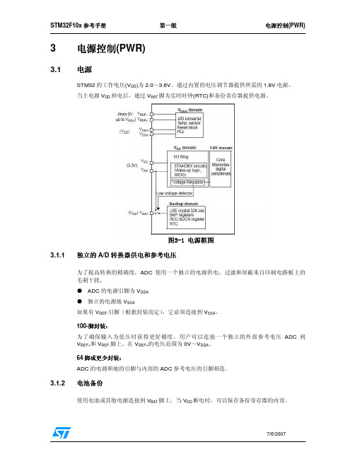
3.1 电源
STM32 的工作电压(VDD)为 2.0~3.6V。通过内置的电压调节器提供所需的 1.8V 电源。 当主电源 VDD 掉电后,通过 VBAT 脚为实时时钟(RTC)和备份寄存器提供电源。
3.1.1
图3-1 电源框图 独立的 A/D 转换器供电和参考电压
如果应用中没有使用外部电池,VBAT 必须连接到 VDD 引脚上。
注意:在 VDD 上升阶段(tRSTTEMPO),VBAT 和 VDD 之间的电源开关仍会保持连接在 VBAT。当 VDD 快速上升且达 到稳定状态,当 VBAT 低于 VDD−0.6V 时,电流通过 VDD 和 VBAT 之间的二极管流入到 VBAT。关于 tRSTTEMPO 可参考数据手册中的相关部分。
STM32f10固件库使用手册中文版
UM0427 用户手册32 位基于ARM 微控制器STM32F101xx 与STM32F103xx固件函数库介绍本手册介绍了32 位基于ARM 微控制器STM32F101xx 与STM32F103xx 的固件函数库。
该函数库是一个固件函数包,它由程序、数据结构和宏组成,包括了微控制器所有外设的性能特征。
该函数库还包括每一个外设的驱动描述和应用实例。
通过使用本固件函数库,无需深入掌握细节,用户也可以轻松应用每一个外设。
因此,使用本固态函数库可以大大减少用户的程序编写时间,进而降低开发成本。
每个外设驱动都由一组函数组成,这组函数覆盖了该外设所有功能。
每个器件的开发都由一个通用API (application programming interface 应用编程界面)驱动,API 对该驱动程序的结构,函数和参数名称都进行了标准化。
所有的驱动源代码都符合“Strict ANSI-C”标准(项目于范例文件符合扩充ANSI-C 标准)。
我们已经把驱动源代码文档化,他们同时兼容MISRA-C 2004 标准(根据需要,我们可以提供兼容矩阵)。
由于整个固态函数库按照“Strict ANSI-C”标准编写,它不受不同开发环境的影响。
仅对话启动文件取决于开发环境。
该固态函数库通过校验所有库函数的输入值来实现实时错误检测。
该动态校验提高了软件的鲁棒性。
实时检测适合于用户应用程序的开发和调试。
但这会增加了成本,可以在最终应用程序代码中移去,以优化代码大小和执行速度。
想要了解更多细节,请参阅Section 2.5。
因为该固件库是通用的,并且包括了所有外设的功能,所以应用程序代码的大小和执行速度可能不是最优的。
对大多数应用程序来说,用户可以直接使用之,对于那些在代码大小和执行速度方面有严格要求的应用程序,该固件库驱动程序可以作为如何设置外设的一份参考资料,根据实际需求对其进行调整。
此份固件库用户手册的整体架构如下:定义,文档约定和固态函数库规则。
- 1、下载文档前请自行甄别文档内容的完整性,平台不提供额外的编辑、内容补充、找答案等附加服务。
- 2、"仅部分预览"的文档,不可在线预览部分如存在完整性等问题,可反馈申请退款(可完整预览的文档不适用该条件!)。
- 3、如文档侵犯您的权益,请联系客服反馈,我们会尽快为您处理(人工客服工作时间:9:00-18:30)。
1/30文档ID 022910第1版2012年3月 STM32F0DISCOVERY STM32F0探索套件UM1525前言STM32F0DISCOVERY 是意法半导体STM32F0系列微控制器的探索套件,用于帮助你探索STM32F0 Cortex-M0微控制器的功能,轻松开发应用设计。
STM32F0探索套件基于1颗STM32F051R8T6微控制器,组件包括ST-LINK/V2嵌入式调试工具、LED 指示灯、按键和1个原型板。
图1: STM32F0探索套件用户手册2/30UM1525文档ID 022910第1版目录目录1. 约定 (5)2. 快速入门 (6)2.1 开始使用 (6)2.2 系统要求 (6)2.3 支持STM32F0探索套件的开发工具链 (6)2.4 订货代码 (6)3. 特性 (7)4. 硬件与原理图 (8)4.1 STM32F051R8T6 微控制器 (11)4.2 嵌入式ST-LINK/V2编程器/调试器 (13)4.2.1 使用ST-LINK/V2向板载STM32F0烧录和调试代码 (14)4.2.2 使用ST-LINK/V2向外部STM32应用板烧录和调试代码 (15)4.3电源和电源选择 (16)4.4 LED指示灯 (16)4.5 按键 (16)4.6 JP2(Idd)﹍﹍﹍﹍﹍﹍﹍﹍﹍﹍﹍﹍﹍﹍﹍﹍﹍﹍﹍﹍﹍﹍﹍164.7 OSC 时钟-----------------------------------------------------------------------------174.7.1 OSC时钟电源 (17)4.7.2 OSC 32kHz时钟电源174.8 焊桥 (18)4.9 扩展连接器 (19)5. 尺寸图 (26)6. 原理图 (27)7. 修改历史记录 (30)3/30文档ID 022910第1版图表目录UM1525表格目录表1:通断约定 (5)表2:跳线状态 (13)表3:调试接口CN2(SWD) (15)表4:焊桥 (18)表5:微控制器引脚与电路板功能 (19)表6:文档修订历史记录 (30)4/30文档ID 022910第1版图形目录UM1525图形目录图1:STM32F0探索套件 (1)图2:硬件框图 (8)图3:电路板正面示意图 (9)图4:电路板背面示意图 ..................................................................................................10图5:STM32F051R8T6封装﹍﹍﹍﹍﹍﹍﹍﹍﹍﹍﹍﹍﹍﹍﹍﹍﹍﹍﹍﹍﹍﹍ 11图6:STM32F051R8T6框图﹍﹍﹍﹍﹍﹍﹍﹍﹍﹍﹍﹍﹍﹍﹍﹍﹍﹍﹍﹍﹍﹍ 12图7:典型配置 (13)图8:STM32F0探索套件接口图 (14)图9:ST-Link 接口图 (15)图10:STM32F0探索套件尺寸图 ..................................................................................26图11:STM32F0探索套件原理图﹍﹍﹍﹍﹍﹍﹍﹍﹍﹍﹍﹍﹍﹍﹍﹍﹍﹍﹍﹍ 27图12:ST-LINK/V2(仅SWD)﹍﹍﹍﹍﹍﹍﹍﹍﹍﹍﹍﹍﹍﹍﹍﹍﹍﹍﹍﹍﹍﹍ 28图13:微控制器 (29)5/30文档ID 022910第1版约定UM15251. 约定下表列出了本文档中某些约定的定义表1 通断约定约定定义跳线JP1接通插入跳线帽跳线JP1关断拆除跳线帽焊桥SBx 接通通过焊接使焊桥使SBx 闭路焊桥SBx 关断焊桥SBx 开路6/30文档ID 022910第1版快速入门UM15252 快速入门STM32F0探索套件是一套高性价比且简单易用的开发工具,能够让开发人员快速评估STM32F0高性能微控制器,并利用这款微控制器的先进功能开发应用设计。
在安装使用本产品前,须在/STM32Ff0discovery 网页接受“评估产品许可协议”。
若想详细了解STM32F0探索套件信息,下载应用演示软件,请访问/STM32f0discovery 。
2.1 开始使用按照下列步骤配置STM32F0探索套件评估板,启动DISCOVERY 应用演示程序:1. 检查板上跳线开关状态,如果选择DISCOVERY 模式,闭路跳线JP2和CN2 ;2. 用一条标准A 型接口转mini-B 型接口的USB 数据线连接PC 机和STM32F0探索套件评估板的USB 接口CN1,通过PC 机电源给评估板供电,这时红光LED 指示灯LD1 (PWR) 和LD2(COM )亮,绿光LED 指示灯LD3闪烁;3. 按用户按键B1(在板子的左下角);4. 观察用户按键B1被按下后绿光LED 指示灯 LD3闪烁频率是如何变化的;5. 每按一次用户按键B1,蓝光LED 指示灯LD4闪烁一次。
6. 若想研究或修改探索演示项目,请访问ST 网站 /STM32f0discovery ,按照使用教程操作;7. 探索STM32F0功能,请下载并执行项目清单所列程序;8. 使用现有固件示例开发自己的应用设计2.2 系统要求·Windows PC (XP/Vista/7)· USB A 口转Mini-B 口数据线2.3 支持STM32F0探索套件的开发工具链·Altium, TASKING ™ VX-Toolset·Atollic ,TrueSTUDiO·IAR, EWARM·Keil ™,MDK-ARM 2.4 订货代码在订购STM32F0高性能探索板时,订货代码请使用STM32F0DISCOVERY 。
7/30文档ID 022910第1版8/30文档ID 022910第1版UM1525硬件和示意图4. 硬件与示意图STM32F0探索套件搭载一颗64引脚LQFP 封装的STM32F051R8T6微控制器。
图2所示是STM32F051R8T6与外设的连接示意图,外设包括ST-LIN K/V2在线调试器/编程器、按键、LED 指示灯和通信接口。
图3和图4帮助你探索STM32F0探索套件的这些功能。
图2: 硬件框图9/30文档ID 022910第1版UM1525硬件和示意图图3: 电路板正面示意图注: CN2、CN3、JP1、P1和P2接口的1号引脚有一个方形标识10/30文档ID 022910第1版UM1525硬件和示意图图4: 电路板背面示意图4.1 STM32F051R8T6 微控制器这是一款搭载ARM TM内核的中低容量的32位微控制器,内置64KB的闪存、8KB RAM、RTC、定时器、ADC、DAC、电压比较和通信接口。
图5: STM32F051R8T6封装STM32F0系列让8位和16位微控制器市场上的客户享受32位微控制器的先进性能和STM32的DNA。
STM32生态系统让STM32成为微控制器市场标杆,同样,STM32F0的成功经验受益于STM32生态系统的实时性能、低动态功耗、先进架构、外设接口。
现在,即便成本敏感市场也同样可获得这些先进功能。
STM32F0让家庭娱乐产品、家电和工业控制设备具有最佳的设计灵活性和扩展性能。
该系列微控制器具有以下优点:•代码执行速度出色,让应用性能更加优异,代码效率更高,降低内存占用率•连接性能优异,先进模拟外设,支持各种应用•灵活的可选的时钟源,支持快速唤醒的低功耗模式,进一步降低动态功耗主要特性和功能:•内核和工作条件– ARM®Cortex™-M0 0.9 DMIPS/MHz,最高48 MHz– 1.8/2.0到3.6 V电源电压•连接性能优异– 6 Mbit/s USART– 18 Mbit/s SPI,数据帧长度在4和16位之间可灵活配置– 1 Mbit/s I2C快速模式+– HDMI CEC•增强控制功能– 1个16位3相电机PWM控制定时器– 5个16位PWM定时器– 1个16位基本定时器– 1个32位PWM定时器– I/O翻转频率高达12 MHz图6: STM32F051R8T6框图4.2 嵌入式ST-LINK/V2编程器及调试器STM32F0探索套件在电路板上集成了ST-LINK/V2编程器及调试器。
根据跳线状态设置(见表2),ST-LINK/V2有两种不同的使用方法:•向板载微控制器写入代码并进行相应的调试操作;•用一条数据线连接SWD接口CN3,对外部应用电路板上的微控制器进行代码烧录和调试操作;这个嵌入式ST-LINK/V2工具只支持通过SWD接口调试STM32微控制器。
若想了解调试和编程的详细功能,请查阅用户手册UM1075 (ST-LINK/V2 STM8和 STM32在线调试器/编程器)。
图7: 典型配置表2 跳线状态跳线状态描述两个CN2跳线都接通ST-LINK/V2对电路板上微控制器进行代码烧录和调试操作两个CN2跳线都关断通过外部连接器CN3(SWD接口支持)对外部应用电路板上的微控制进行代码烧录和调试操作4.2.1 使用ST-LINK/V2向板载STM32F0烧录和调试代码只要把把两个跳线帽插入CN2接口,即可开启探索套件板向板载STM32F0烧录代码的功能,如图8所示。
请勿跳CN3接口,因为这可能会干扰ST-LINK/ V2与STM32F0探索套件上的STM32F051R8T6的通信功能。
图8: STM32F0探索套件接口图4.2.2 使用ST-LINK/V2向外部STM32应用板烧录和调试代码使用ST-LINK/V2向外部STM32应用板烧录和调试代码非常简单,只要拆除CN2上的两个跳线帽,如图9所示,然后按照表3所列引脚顺序,把外部应用连接到CN3调试接口即可。
注: 如果使用CN3的5号引脚连接外部应用电路板,SB19和SB22必须断开。
表3 调试接口CN3(SWD)引脚CN3引脚分配1VDD_TARGET外部应用板的VDD电压2SWCLK SWD时钟3 接地接地4SWDIO SWD数据输入/输出5 NRST 目标微控制器复位6SWO保留图9: ST-Link接口图图9 ST-Link接口图4.3 电源和电源选择STM32F0探索套件可以通过USB数据线使用PC机的电源,也可以使用一个外部5V电源。
二极管D1和D2用于保护5V和3V针脚,防止部电源的电涌冲击:•当另一个应用板连接到引脚P1和P2时,5V和3V引脚可用作输出电源;在这种情况下,P1和P2引脚可为外部应用提供5V电源,但是,电流消耗必须小于100mA;•当USB接口没有连接PC机时,5V引脚还可以用作输入电源。